

Burr Brown OPA124UA, OPA124UA-2K5, OPA124U-2K5, OPA124U, OPA124PB Datasheet
...
®
OPA124
1
FEATURES
● LOW NOISE: 6nV/√Hz (10kHz)
● LOW BIAS CURRENT: 1pA max
● LOW OFFSET: 250
µV max
● LOW DRIFT: 2
µV/°C max
● HIGH OPEN-LOOP GAIN: 120dB min
● HIGH COMMON-MODE REJECTION:
100dB min
● AVAILABLE IN 8-PIN PLASTIC DIP
AND 8-PIN SOIC PACKAGES
APPLICATIONS
● PRECISION PHOTODIODE PREAMP
● MEDICAL EQUIPMENT
● OPTOELECTRONICS
● DATA ACQUISITION
● TEST EQUIPMENT
OPA124
DESCRIPTION
The OPA124 is a precision monolithic FET operational amplifier using a
Difet
(dielectrical isolation)
manufacturing process. Outstanding DC and AC performance characteristics allow its use in the most
critical instrumentation applications.
Bias current, noise, voltage offset, drift, open-loop
gain, common-mode rejection and power supply rejection are superior to BIFET and CMOS amplifiers.
Difet
fabrication achieves extremely low input bias
currents without compromising input voltage noise
performance. Low input bias current is maintained
over a wide input common-mode voltage range with
unique cascode circuitry. This cascode design also
allows high precision input specifications and reduced
susceptibility to flicker noise. Laser trimming of thinfilm resistors gives very low offset and drift.
Compared to the popular OPA111, the OPA124 gives
comparable performance and is available in an 8-pin
PDIP and 8-pin SOIC package.
BIFET® National Semiconductor Corp.,
Difet
®
Burr-Brown Corp.
®
Low Noise Precision
Difet
®
OPERATIONAL AMPLIFIER
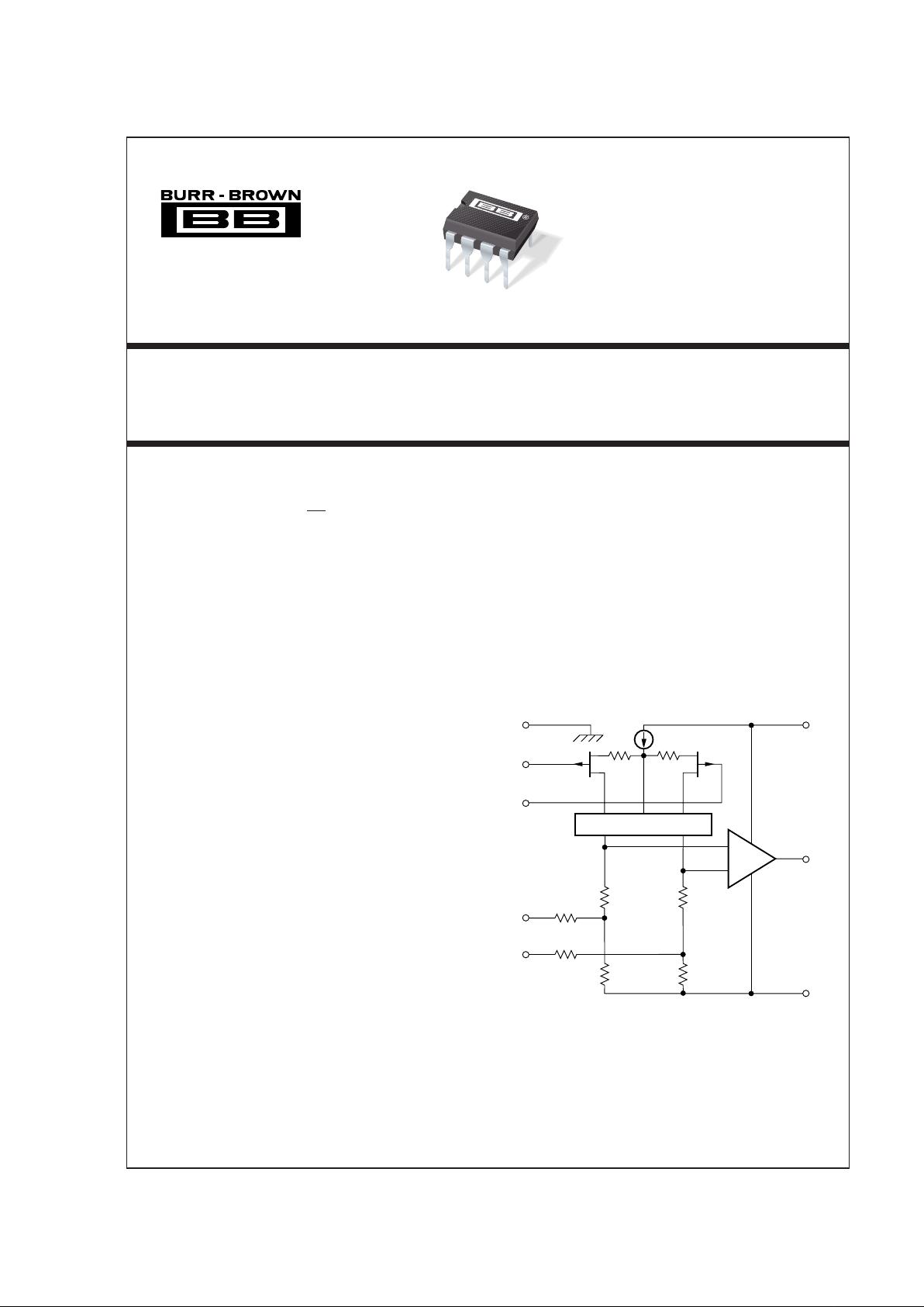
8
2
3
1
5
7
6
4
Substrate
Output
Trim
(1)
+V
CC
Noise-Free Cascode
(2)
Trim
(1)
+In
–In
–V
CC
2kΩ
2kΩ
2kΩ
10kΩ
10kΩ
NOTES: (1) Omitted on SOIC. (2) Patented.
2kΩ
OPA124 Simplified Circuit
International Airport Industrial Park • Mailing Address: PO Box 11400, Tucson, AZ 85734 • Street Address: 6730 S. Tucson Blvd., Tucson, AZ 85706 • Tel: (520) 746-1111 • Twx: 910-952-1111
Internet: http://www.burr-brown.com/ • FAXLine: (800) 548-6133 (US/Canada Only) • Cable: BBRCORP • Telex: 066-6491 • FAX: (520) 889-1510 • Immediate Product Info: (800) 548-6132
© 1993 Burr-Brown Corporation PDS-1203C Printed in U.S.A. March, 1998
OPA124
®
OPA124
2
SPECIFICATIONS
ELECTRICAL
At V
CC
= ±15VDC and TA = +25°C, unless otherwise noted.
OPA124U, P OPA124UA, PA OPA124PB
PARAMETER CONDITION MIN TYP MAX MIN TYP MAX MIN TYP MAX UNITS
INPUT NOISE
Voltage,f
O
= 10Hz
(4)
40 80 ✻✻ ✻✻nV/√Hz
f
O
= 100Hz
(4)
15 40 ✻✻ ✻✻nV/√Hz
f
O
= 1kHz
(4)
815 ✻✻ ✻✻nV/√Hz
f
O
= 10kHz
(5)
68 ✻✻ ✻✻nV/√Hz
f
B
= 10Hz to 10kHz
(5)
0.7 1.2 ✻✻ ✻✻µVrms
f
B
= 0.1Hz to 10Hz 1.6 3.3 ✻✻ ✻✻µVp-p
Current, f
B
= 0.1Hz to 10Hz 9.5 15 ✻✻ ✻✻fAp-p
f
O
= 0.1Hz thru 20kHz 0.5 0.8 ✻✻ ✻✻fA/√Hz
OFFSET VOLTAGE
(1)
Input Offset Voltage VCM = 0VDC ±200 ±800 ±150 ±500 ±100 ±250 µV
vs Temperature T
A
= T
MIN
to T
MAX
±4 ±7.5 ±2 ±4 ±1 ±2 µV/°C
Supply Rejection V
CC
= ±10V to ±18V 88 110 90 ✻ 100 ✻ dB
vs Temperature T
A
= T
MIN
to T
MAX
84 100 86 ✻ 90 ✻ dB
BIAS CURRENT
(1)
Input Bias Current VCM = 0VDC ±1 ±5 ±0.5 ±2 ±0.35 ±1pA
OFFSET CURRENT
(1)
Input Offset Current VCM = 0VDC ±1 ±5 ±0.5 ±1 ±0.25 ±0.5 pA
IMPEDANCE
Differential 10
13
|| 1 ✻✻Ω || pF
Common-Mode 10
14
|| 3 ✻✻Ω || pF
VOLTAGE RANGE
Common-Mode Input Range ±10 ±11 ✻✻ ✻✻ V
Common-Mode Rejection V
IN
= ±10VDC 92 110 94 ✻ 100 ✻ dB
vs Temperature T
A
= T
MIN
to T
MAX
86 100 ✻✻ 90 ✻ dB
OPEN-LOOP GAIN, DC
Open-Loop Voltage Gain R
L
≥ 2kΩ 106 125 ✻✻ 120 ✻ dB
FREQUENCY RESPONSE
Unity Gain, Small Signal 1.5 ✻✻MHz
Full Power Response 20Vp-p, R
L
= 2kΩ 16 32 ✻✻ ✻✻ kHz
Slew Rate V
O
= ±10V, RL = 2kΩ 1 1.6 ✻✻ ✻✻ V/µs
THD 0.0003 ✻✻%
Settling Time, 0.1% Gain = –1, R
L
= 2kΩ 6 ✻✻µs
0.01% 10V Step 10 ✻✻µs
Overload Recovery,
50% Overdrive
(2)
Gain = –1 5 ✻✻µs
RATED OUTPUT
Voltage Output R
L
= 2kΩ±11 ±12 ✻✻ ✻✻ V
Current Output V
O
= ±10VDC ±5.5 ±10 ✻✻ ✻✻ mA
Output Resistance DC, Open Loop 100 ✻✻Ω
Load Capacitance Stability Gain = +1 1000 ✻✻pF
Short Circuit Current 10 40 ✻✻ ✻✻ mA
POWER SUPPLY
Rated Voltage ±15 ✻✻VDC
Voltage Range, Derated ±5 ±18 ✻✻✻✻VDC
Current, Quiescent I
O
= 0mADC 2.5 3.5 ✻✻ ✻✻mA
TEMPERATURE RANGE
Specification T
MIN
and T
MAX
–25 +85 ✻✻✻✻°C
Storage –65 +125 ✻✻✻✻°C
θ
Junction-Ambient: PDIP 90 ✻✻°C/W
SOIC 100 ✻✻°C/W
✻ Specification same as OPA124U, P
NOTES: (1) Offset voltage, offset current, and bias current are measured with the units fully warmed up. For performance at other temperatures see Typical Performance
Curves. (2) Overload recovery is defined as the time required for the output to return from saturation to linear operation following the removal of a 50% input overdrive.
(3) For performance at other temperatures see Typical Performance Curves. (4) Sample tested, 98% confidence. (5) Guaranteed by design.
®
OPA124
3
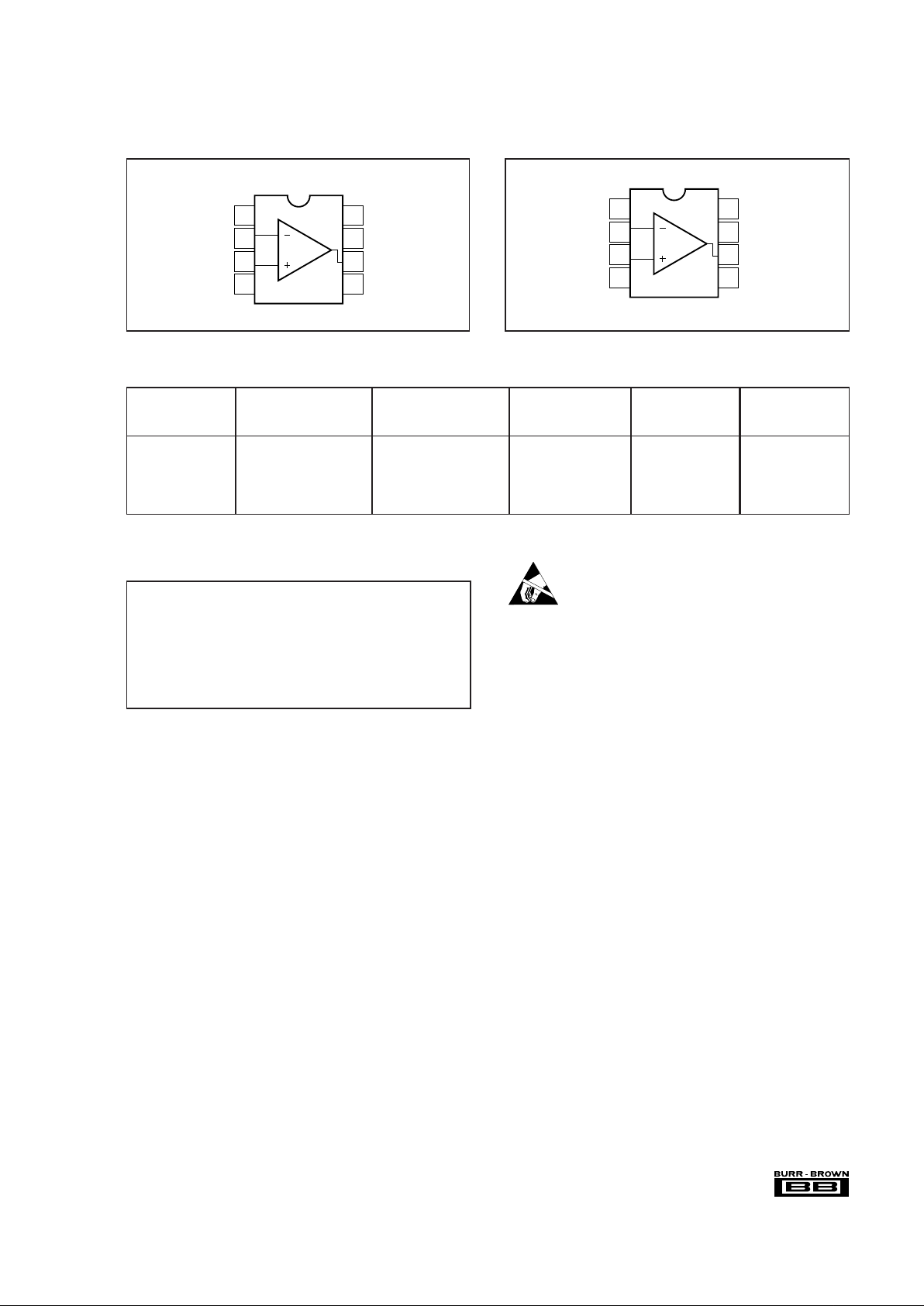
CONNECTION DIAGRAMS
Top View DIP
1
2
3
4
8
7
6
5
Substrate
+V
S
Output
Offset Trim
Offset Trim
–In
+In
–V
S
Top View SOIC
1
2
3
4
8
7
6
5
Substrate
+V
S
Output
NC
NC
–In
+In
–V
S
NC = No Connect
The information provided herein is believed to be reliable; however, BURR-BROWN assumes no responsibility for inaccuracies or omissions. BURR-BROWN assumes
no responsibility for the use of this information, and all use of such information shall be entirely at the user’s own risk. Prices and specifications are subject to change
without notice. No patent rights or licenses to any of the circuits described herein are implied or granted to any third party. BURR-BROWN does not authorize or warrant
any BURR-BROWN product for use in life support devices and/or systems.
PACKAGE/ORDERING INFORMATION
BIAS OFFSET
PACKAGE TEMPERATURE CURRENT DRIFT
PRODUCT PACKAGE DRAWING NUMBER
(1)
RANGE pA, max µV/° C, max
OPA124U 8-Lead SOIC 182 –25°C to +85°C 5 7.5
OPA124P 8-Pin Plastic DIP 006 –25°C to +85°C 5 7.5
OPA124UA 8-Lead SOIC 182 –25°C to +85°C2 4
OPA124PA 8-Pin Plastic DIP 006 –25°C to +85°C2 4
OPA124PB 8-Pin Plastic DIP 006 –25°C to +85°C1 2
NOTE: (1) For detailed drawing and dimension table, please see end of data sheet, or Appendix C of Burr-Brown IC Data Book.
ABSOLUTE MAXIMUM RATINGS
(1)
Supply ........................................................................................... ±18VDC
Internal Power Dissipation
(2)
......................................................... 750mW
Differential Input Voltage
(3)
..........................................................±36VDC
Input Voltage Range
(3)
.................................................................±18VDC
Storage Temperature Range .......................................... –65°C to +150°C
Operating Temperature Range ....................................... –40°C to +125°C
Lead Temperature (soldering, 10s)................................................ +300°C
Output Short Circuit Duration
(4)
............................................... Continuous
Junction Temperature .................................................................... +175°C
NOTES: (1) Stresses above these ratings may cause permanent damage.
(2) Packages must be derated based on
θ
JA
= 90°C/W for PDIP and 100°C/W
for SOIC. (3) For supply voltages less than ±18VDC, the absolute maximum
input voltage is equal to +18V > V
IN
> –VCC – 6V. See Figure 2. (4) Short circuit
may be to power supply common only. Rating applies to +25°C ambient.
Observe dissipation limit and T
J
.
ELECTROSTATIC
DISCHARGE SENSITIVITY
This integrated circuit can be damaged by ESD. Burr-Brown
recommends that all integrated circuits be handled with
appropriate precautions. Failure to observe proper handling
and installation procedures can cause damage.
ESD damage can range from subtle performance degradation to complete device failure. Precision integrated circuits
may be more susceptible to damage because very small
parametric changes could cause the device not to meet its
published specifications.
 Loading...