

Page 1
查询OPA124供应商
®
Low Noise Precision
OPERATIONAL AMPLIFIER
FEATURES
● LOW NOISE: 6nV/√Hz (10kHz)
● LOW BIAS CURRENT: 1pA max
● LOW OFFSET: 250
● LOW DRIFT: 2
● HIGH OPEN-LOOP GAIN: 120dB min
● HIGH COMMON-MODE REJECTION:
100dB min
● AVAILABLE IN 8-PIN PLASTIC DIP
AND 8-PIN SOIC PACKAGES
DESCRIPTION
The OPA124 is a precision monolithic FET operational amplifier using a
manufacturing process. Outstanding DC and AC performance characteristics allow its use in the most
critical instrumentation applications.
Bias current, noise, voltage offset, drift, open-loop
gain, common-mode rejection and power supply rejection are superior to BIFET and CMOS amplifiers.
Difet
fabrication achieves extremely low input bias
currents without compromising input voltage noise
performance. Low input bias current is maintained
over a wide input common-mode voltage range with
unique cascode circuitry. This cascode design also
allows high precision input specifications and reduced
susceptibility to flicker noise. Laser trimming of thinfilm resistors gives very low offset and drift.
Compared to the popular OPA111, the OPA124 gives
comparable performance and is available in an 8-pin
PDIP and 8-pin SOIC package.
BIFET® National Semiconductor Corp.,
®
Difet
Burr-Brown Corp.
µV max
µV/°C max
Difet
(dielectrical isolation)
OPA124
OPA124
Difet
APPLICATIONS
● PRECISION PHOTODIODE PREAMP
● MEDICAL EQUIPMENT
● OPTOELECTRONICS
● DATA ACQUISITION
● TEST EQUIPMENT
Substrate
8
–In
2
+In
3
(1)
Trim
1
(1)
Trim
5
NOTES: (1) Omitted on SOIC. (2) Patented.
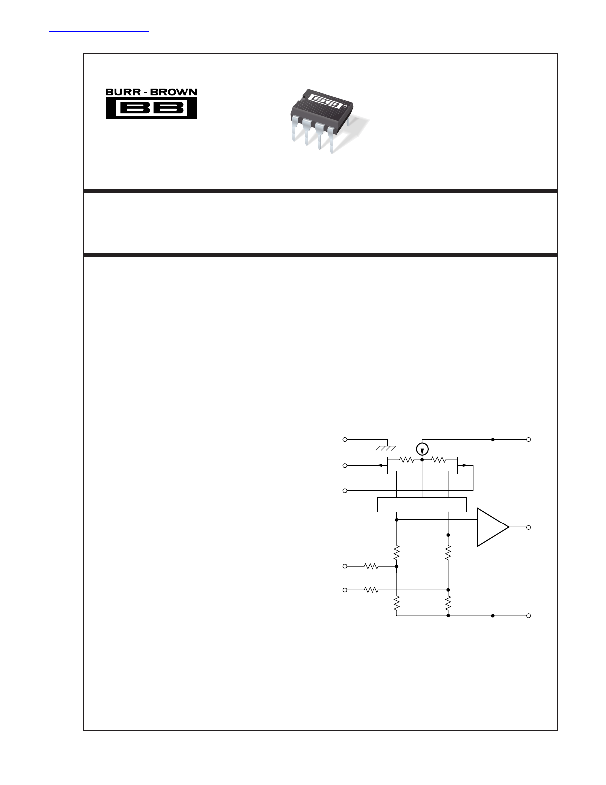
Noise-Free Cascode
10kΩ
10kΩ
2kΩ
2kΩ
OPA124 Simplified Circuit
®
(2)
2kΩ
2kΩ
+V
CC
7
Output
6
–V
CC
4
International Airport Industrial Park • Mailing Address: PO Box 11400, Tucson, AZ 85734 • Street Address: 6730 S. Tucson Blvd., Tucson, AZ 85706 • Tel: (520) 746-1111 • Twx: 910-952-1111
Internet: http://www.burr-brown.com/ • FAXLine: (800) 548-6133 (US/Canada Only) • Cable: BBRCORP • Telex: 066-6491 • FAX: (520) 889-1510 • Immediate Product Info: (800) 548-6132
®
© 1993 Burr-Brown Corporation PDS-1203C Printed in U.S.A. March, 1998
1
OPA124
Page 2

SPECIFICATIONS
ELECTRICAL
At V
= ±15VDC and TA = +25°C, unless otherwise noted.
CC
OPA124U, P OPA124UA, PA OPA124PB
PARAMETER CONDITION MIN TYP MAX MIN TYP MAX MIN TYP MAX UNITS
INPUT NOISE
Voltage,f
Current, f
OFFSET VOLTAGE
Input Offset Voltage VCM = 0VDC ±200 ±800 ±150 ±500 ±100 ±250 µV
vs Temperature T
Supply Rejection V
vs Temperature T
BIAS CURRENT
Input Bias Current VCM = 0VDC ±1 ±5 ±0.5 ±2 ±0.35 ±1pA
OFFSET CURRENT
Input Offset Current VCM = 0VDC ±1 ±5 ±0.5 ±1 ±0.25 ±0.5 pA
IMPEDANCE
Differential 10
Common-Mode 10
VOLTAGE RANGE
Common-Mode Input Range ±10 ±11 ✻✻ ✻✻ V
Common-Mode Rejection V
vs Temperature T
OPEN-LOOP GAIN, DC
Open-Loop Voltage Gain R
FREQUENCY RESPONSE
Unity Gain, Small Signal 1.5 ✻✻MHz
Full Power Response 20Vp-p, R
Slew Rate V
THD 0.0003 ✻✻%
Settling Time, 0.1% Gain = –1, R
0.01% 10V Step 10 ✻✻µs
Overload Recovery,
50% Overdrive
RATED OUTPUT
Voltage Output R
Current Output V
Output Resistance DC, Open Loop 100 ✻✻Ω
Load Capacitance Stability Gain = +1 1000 ✻✻pF
Short Circuit Current 10 40 ✻✻ ✻✻ mA
POWER SUPPLY
Rated Voltage ±15 ✻✻VDC
Voltage Range, Derated ±5 ±18 ✻✻✻✻VDC
Current, Quiescent I
TEMPERATURE RANGE
Specification T
Storage –65 +125 ✻✻✻✻°C
θ
Junction-Ambient: PDIP 90 ✻✻°C/W
SOIC 100 ✻✻°C/W
✻ Specification same as OPA124U, P
NOTES: (1) Offset voltage, offset current, and bias current are measured with the units fully warmed up. For performance at other temperatures see Typical Performance
Curves. (2) Overload recovery is defined as the time required for the output to return from saturation to linear operation following the removal of a 50% input overdrive.
(3) For performance at other temperatures see Typical Performance Curves. (4) Sample tested, 98% confidence. (5) Guaranteed by design.
(4)
= 10Hz
O
f
O
f
O
f
O
f
B
f
B
B
f
O
(4)
= 100Hz
(4)
= 1kHz
(5)
= 10kHz
= 10Hz to 10kHz
(5)
= 0.1Hz to 10Hz 1.6 3.3 ✻✻ ✻✻µVp-p
= 0.1Hz to 10Hz 9.5 15 ✻✻ ✻✻fAp-p
= 0.1Hz thru 20kHz 0.5 0.8 ✻✻ ✻✻fA/√Hz
(1)
= T
to T
A
MIN
= ±10V to ±18V 88 110 90 ✻ 100 ✻ dB
CC
= T
(1)
(1)
(2)
A
IN
= T
A
= ±10V, RL = 2kΩ 1 1.6 ✻✻ ✻✻ V/µs
O
O
O
MAX
MIN
to T
MAX
84 100 86 ✻ 90 ✻ dB
= ±10VDC 92 110 94 ✻ 100 ✻ dB
to T
MIN
MAX
≥ 2kΩ 106 125 ✻✻ 120 ✻ dB
L
= 2kΩ 16 32 ✻✻ ✻✻ kHz
L
= 2kΩ 6 ✻✻µs
L
86 100 ✻✻ 90 ✻ dB
Gain = –1 5 ✻✻µs
= 2kΩ±11 ±12 ✻✻ ✻✻ V
L
= ±10VDC ±5.5 ±10 ✻✻ ✻✻ mA
= 0mADC 2.5 3.5 ✻✻ ✻✻mA
MIN
and T
MAX
–25 +85 ✻✻✻✻°C
40 80 ✻✻ ✻✻nV/√Hz
15 40 ✻✻ ✻✻nV/√Hz
815 ✻✻ ✻✻nV/√Hz
68 ✻✻ ✻✻nV/√Hz
0.7 1.2 ✻✻ ✻✻µVrms
±4 ±7.5 ±2 ±4 ±1 ±2 µV/°C
13
|| 1 ✻✻Ω || pF
14
|| 3 ✻✻Ω || pF
®
OPA124
2
Page 3
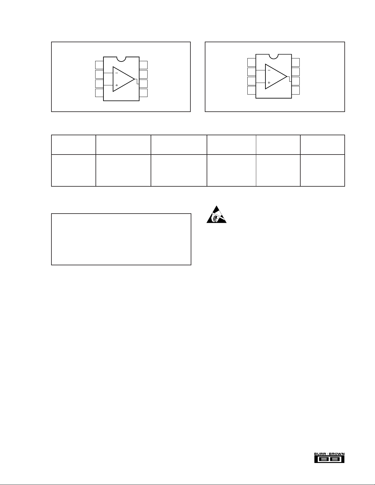
CONNECTION DIAGRAMS
Top View DIP
Top View SOIC
Offset Trim
–In
+In
–V
1
–V
NC
–In
+In
2
3
4
S
NC = No Connect
1
2
3
4
S
8
7
6
5
Substrate
+V
S
Output
Offset Trim
8
7
6
5
Substrate
+V
S
Output
NC
PACKAGE/ORDERING INFORMATION
PRODUCT PACKAGE DRAWING NUMBER
OPA124U 8-Lead SOIC 182 –25°C to +85°C 5 7.5
OPA124P 8-Pin Plastic DIP 006 –25°C to +85°C 5 7.5
OPA124UA 8-Lead SOIC 182 –25°C to +85°C2 4
OPA124PA 8-Pin Plastic DIP 006 –25°C to +85°C2 4
OPA124PB 8-Pin Plastic DIP 006 –25°C to +85°C1 2
NOTE: (1) For detailed drawing and dimension table, please see end of data sheet, or Appendix C of Burr-Brown IC Data Book.
ABSOLUTE MAXIMUM RATINGS
Supply ........................................................................................... ±18VDC
Internal Power Dissipation
Differential Input Voltage
Input Voltage Range
Storage Temperature Range .......................................... –65°C to +150°C
Operating Temperature Range ....................................... –40°C to +125°C
Lead Temperature (soldering, 10s)................................................ +300°C
Output Short Circuit Duration
Junction Temperature .................................................................... +175°C
NOTES: (1) Stresses above these ratings may cause permanent damage.
(2) Packages must be derated based on
for SOIC. (3) For supply voltages less than ±18VDC, the absolute maximum
input voltage is equal to +18V > V
may be to power supply common only. Rating applies to +25°C ambient.
Observe dissipation limit and T
(2)
......................................................... 750mW
(3)
..........................................................±36VDC
(3)
.................................................................±18VDC
(4)
............................................... Continuous
> –VCC – 6V. See Figure 2. (4) Short circuit
IN
.
J
(1)
θ
= 90°C/W for PDIP and 100°C/W
JA
PACKAGE TEMPERATURE CURRENT DRIFT
(1)
RANGE pA, max µV/° C, max
ELECTROSTATIC
DISCHARGE SENSITIVITY
This integrated circuit can be damaged by ESD. Burr-Brown
recommends that all integrated circuits be handled with
appropriate precautions. Failure to observe proper handling
and installation procedures can cause damage.
ESD damage can range from subtle performance degradation to complete device failure. Precision integrated circuits
may be more susceptible to damage because very small
parametric changes could cause the device not to meet its
published specifications.
BIAS OFFSET
The information provided herein is believed to be reliable; however, BURR-BROWN assumes no responsibility for inaccuracies or omissions. BURR-BROWN assumes
no responsibility for the use of this information, and all use of such information shall be entirely at the user’s own risk. Prices and specifications are subject to change
without notice. No patent rights or licenses to any of the circuits described herein are implied or granted to any third party. BURR-BROWN does not authorize or warrant
any BURR-BROWN product for use in life support devices and/or systems.
3
OPA124
®
Page 4

TYPICAL PERFORMANCE CURVES
At TA = +25°C, and VCC = ±15VDC, unless otherwise noted.
100
Current Noise (fA/√Hz)
100
0.1
INPUT CURRENT NOISE SPECTRAL DENSITY
10
1
PB
100101 10k 100k 1M
1k
Frequency (Hz)
(1)
TOTAL
INPUT VOLTAGE NOISE SPECTRAL
DENSITY vs SOURCE RESISTANCE
1k
RS= 10MΩ
RS= 1MΩ
RS= 100kΩ
Voltage Noise (nV/√Hz)
INPUT VOLTAGE NOISE SPECTRAL DENSITY
1k
100
10
PB
1
(1)
TOTAL
INPUT VOLTAGE NOISE (PEAK-TO-PEAK)
1k
NOTE: (1) Includes contribution
100
from source resistance.
U, P
1k
10k 100k 1M100101
Frequency (Hz)
vs SOURCE RESISTANCE
PB
Voltage Noise (nV/√Hz)
10
NOTE: (1) Includes contribution
RS= 100Ω
from source resistance.
1
100
1k 10k 100k1010.1
Frequency (Hz)
VOLTAGE AND CURRENT NOISE SPECTRAL
DENSITY vs TEMPERATURE
12
fO= 1kHz
10
8
6
Voltage Noise (nV/√Hz)
4
–50 –25 0 25 50 75 100 125
Temperature (°C)
100
10
1
0.1
0.01
Current Noise (fA/√Hz)
10
Voltage Noise (µVp-p)
1
4
5
10
10
6
10
10
PB
= 0.1Hz to 10Hz
f
B
7
8
10
Source Resistance (Ω)
TOTAL INPUT VOLTAGE NOISE SPECTRAL DENSITY
AT 1kHz vs SOURCE RESISTANCE
1k
E
O
(nV/√Hz)
O
100
R
S
OPA124PB +
10
Voltage Noise, E
Resistor
Resistor Noise Only
1
100 1k 10k 100k 1M 10M 100M
Source Resistance ( )Ω
9
10
10
10
®
OPA124
4
Page 5

TYPICAL PERFORMANCE CURVES (CONT)
At TA = +25°C, and VCC = ±15VDC, unless otherwise noted.
1k
100
10
1
Bias Current (pA)
0.1
0.01
–50
140
120
100
80
BIAS AND OFFSET CURRENT
vs TEMPERATURE
PB
0 25 50 75 100 125
–25
Ambient Temperature (°C)
POWER SUPPLY REJECTION
vs FREQUENCY
1k
100
10
1
Offset Current (pA)
0.1
0.01
BIAS AND OFFSET CURRENT
10
1
0.1
Bias Current (pA)
0.01
–15 –10 –5 0 5 10 15
140
120
100
80
vs INPUT COMMON-MODE VOLTAGE
Bias Current
Offset Current
Common-Mode Voltage (V)
COMMON-MODE REJECTION
vs FREQUENCY
10
1
0.1
Offset Current (pA)
0.01
60
40
Power Supply Rejection (dB)
20
0
1
10 100 1k 10k 100k 1M 10M
COMMON-MODE REJECTION
120
110
100
90
80
Common-Mode Rejection (dB)
70
–15
vs INPUT COMMON-MODE VOLTAGE
–10 –5 0 5 10 15
Common-Mode Voltage (V)
Frequency (Hz)
60
40
20
Common-Mode Rejection (dB)
0
1
10 100 1k 10k 100k 1M 10M
140
120
100
80
60
Voltage Gain (dB)
40
20
0
OPEN-LOOP FREQUENCY RESPONSE
1
10 100 1k 10k 100k 1M 10M
Frequency (Hz)
Gain
Frequency (Hz)
Phase
Margin
≈ 65°
–45
–90
–135
Phase Shift (Degrees)
–180
®
5
OPA124
Page 6

TYPICAL PERFORMANCE CURVES (CONT)
At TA = +25°C, and VCC = ±15VDC, unless otherwise noted.
GAIN-BANDWIDTH AND SLEW RATE
4
4
3
3
2
2
1
1
Gain Bandwidth (MHz)
0
0
–50 –25 0 25 50 75 100 125
140
130
120
vs TEMPERATURE
Ambient Temperature (°C)
OPEN-LOOP GAIN vs TEMPERATURE
4
3
2
Slew Rate (V/µs)
1
0
GAIN-BANDWIDTH AND SLEW RATE
3
2
1
Gain Bandwidth (MHz)
0
0
30
20
5 101520
MAXIMUM UNDISTORTED OUTPUT
vs SUPPLY VOLTAGE
Supply Voltage (±V
VOLTAGE vs FREQUENCY
)
CC
3
2
1
Slew Rate (V/µs)
0
Voltage Gain (dB)
110
100
–50 –25 0 25 50 75 100 125
Ambient Temperature (°C)
15
10
5
0
–5
Output Voltage (V)
–10
–15
LARGE SIGNAL TRANSIENT RESPONSE
050
10
20 30 40
Time (µs)
10
Output Voltage (Vp-p)
0
1k 10k 1M
60
40
20
0
–20
Output Voltage (mV)
–40
–60
SMALL SIGNAL TRANSIENT RESPONSE
05
1
100k
Frequency (Hz)
234
Time (µs)
®
OPA124
6
Page 7

TYPICAL PERFORMANCE CURVES (CONT)
At TA = +25°C, and VCC = ±15VDC, unless otherwise noted.
100
SETTLING TIME vs CLOSED-LOOP GAIN
80
60
40
Settling Time (µs)
20
0
1
Closed-Loop Gain (V/V)
INPUT OFFSET VOLTAGE WARM-UP DRIFT
20
10
0
–10
Offset Voltage Change (µV)
0.1%0.01%
10 100 1k
4
3
2
Supply Current (mA)
1
0
–50 –25 0 25 50 75 100 125
150
75
0
–75
Offset Voltage Change (µV)
SUPPLY CURRENT vs TEMPERATURE
Ambient Temperature (°C)
INPUT OFFSET VOLTAGE CHANGE
DUE TO THERMAL SHOCK
+25°C +85°C
TA = +25°C to TA = +85°C
U, P
PB
Air Environment
–20
0 123456
Time From Power Turn-On (Minutes)
–150
–1012345
Time From Thermal Shock (Minutes)
®
7
OPA124
Page 8

APPLICATIONS INFORM ATION
OFFSET VOLTAGE ADJUSTMENT
The OPA124 offset voltage is laser-trimmed and will require
no further trim for most applications. In order to reduce
layout leakage errors, the offset adjust capability has been
removed from the SOIC versions (OPA124UA and
OPA124U). The PDIP versions (OPA124PB, OPA124PA,
and OPA124P) do have pins available for offset adjustment.
As with most amplifiers, externally trimming the remaining
offset can change drift performance by about 0.3µV/°C for
each 100µV of adjusted offset. The correct circuit configuration for offset adjust for the PDIP packages is shown in
Figure 1.
INPUT PROTECTION
Conventional monolithic FET operational amplifiers require
external current-limiting resistors to protect their inputs
against destructive currents that can flow when input FET
gate-to-substrate isolation diodes are forward-biased. Most
BIFET amplifiers can be destroyed by the loss of –V
Difet
Unlike BIFET amplifiers, the
OPA124 requires input
current limiting resistors only if its input voltage is greater
than 6V more negative than –VCC. A 10kΩ series resistor
will limit input current to a safe level with up to ±15V input
levels, even if both supply voltages are lost (Figure 2).
Static damage can cause subtle changes in amplifier input
characteristics without necessarily destroying the device. In
precision operational amplifiers (both bipolar and FET types),
this may cause a noticeable degradation of offset voltage and
drift. Static protection is recommended when handling any
precision IC operational amplifier.
GUARDING AND SHIELDING
As in any situation where high impedances are involved,
careful shielding is required to reduce “hum” pickup in input
leads. If large feedback resistors are used, they should also
be shielded along with the external input circuitry.
Leakage currents across printed circuit boards can easily
exceed the bias current of the OPA124. To avoid leakage
problems, the OPA124 should be soldered directly into a
printed circuit board. Utmost care must be used in planning
the board layout. A “guard” pattern should completely
surround the high impedance input leads and should be
connected to a low impedance point which is at the signal
input potential.
The amplifier substrate should be connected to any input
shield or guard via pin 8 minimizing both leakage and noise
pickup (see Figure 3).
If guarding is not required, pin 8 should be connected to
ground.
CC
.
2
OPA124P
3
4
+V
CC
7
6
1
5
10k
Ω to 1MΩ trim potentiometer.
(100k
–V
±10mV typical trim range.
CC
NOTE: No trim on SOIC.
Ω
recommended).
FIGURE 1. Offset Voltage Trim for PDIP packages.
2
I
IN
1
0
Input Current (mA)
–1
–2
–15
V
–10 –5 0 5 10 15
Input Voltage (V)
Maximum Safe Current
Maximum Safe Current
FIGURE 2. Input Current vs Input Voltage with ±VCC Pins
Grounded.
Non-Inverting
2
8
Out
OPA124
In
In
3
Inverting
2
OPA124
3
Board layout for PDIP input guarding: guard top and bottom of board.
6
In
Out
6
8
8
7
6
5
Buffer
2
8
OPA124
3
Bottom View
1
4
Out
6
FIGURE 3. Connection of Input Guard.
®
OPA124
8
 Loading...