

Burr Brown OPA121KM, OPA121KP, OPA121KU, OPA121KU-2K5 Datasheet
Low Cost Precision
Difet
®
OPERATIONAL AMPLIFIER
Difet
®
, Burr-Brown Corp.
BIFET
®
, National Semiconductor Corp.
OPA121
FEATURES
● LOW NOISE: 6nV/√Hz typ at 10kHz
● LOW BIAS CURRENT: 5pA max
● LOW OFFSET: 2mV max
● LOW DRIFT: 3
µV/°C typ
● HIGH OPEN-LOOP GAIN: 110dB min
● HIGH COMMON-MODE
REJECTION: 86dB min
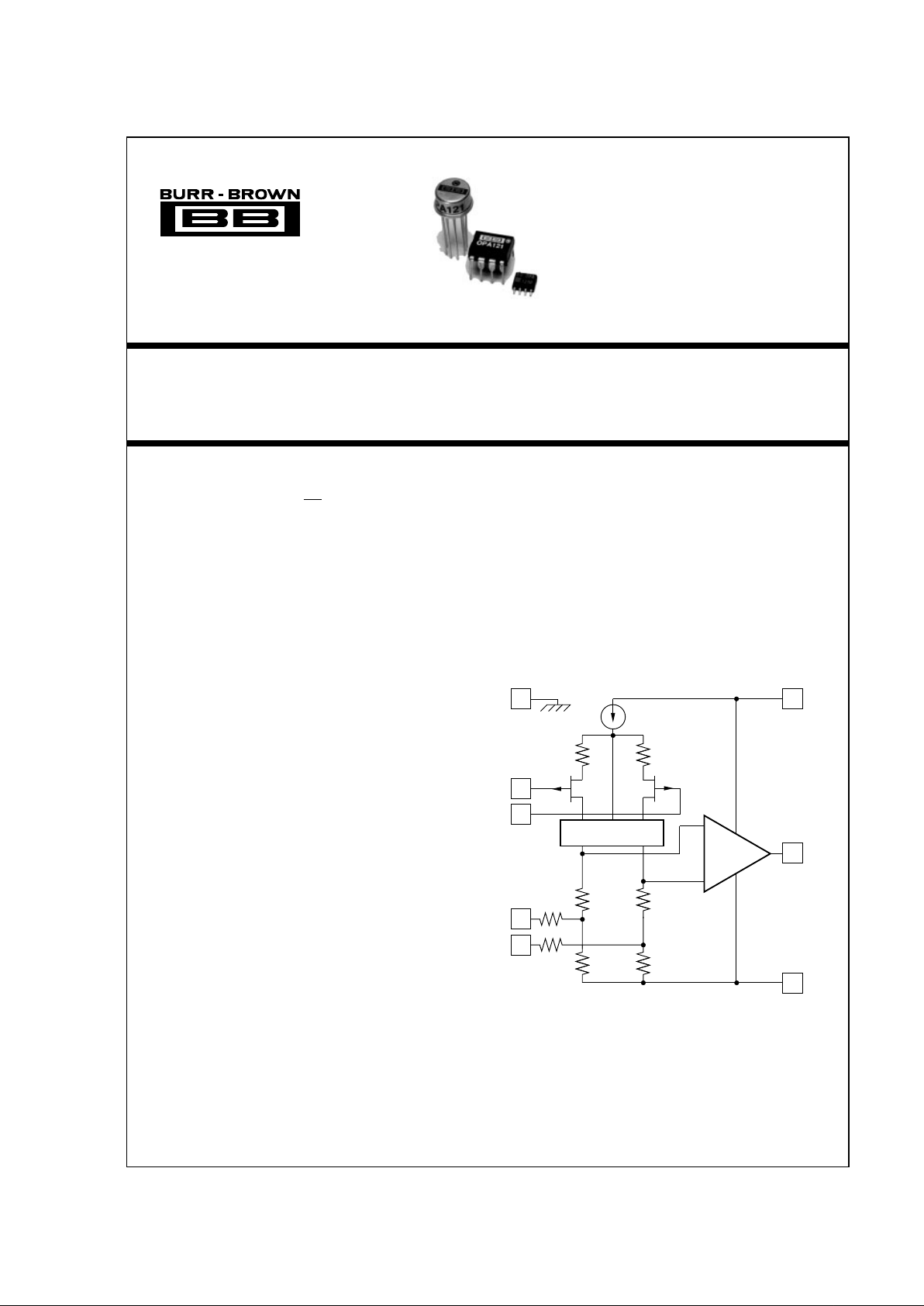
Noise-Free
Cascode*
Ω10k
Trim
1
5
3
2
+In
–In
Case (TO-99) and Substrate
Output
OPA121 Simplified Circuit
+V
CC
–V
CC
8
7
6
4
2kΩ
Ω10k
2kΩ
2kΩ
2kΩ
*Patented
Trim
DESCRIPTION
The OPA121 is a precision monolithic dielectricallyisolated FET (
Difet
®
) operational amplifier. Outstanding performance characteristics are now
available for low-cost applications.
Noise, bias current, voltage offset, drift, open-loop
gain, common-mode rejection, and power supply
rejection are superior to BIFET
®
amplifiers.
Very low bias current is obtained by dielectric
isolation with on-chip guarding.
Laser-trimming of thin-film resistors gives very low
offset and drift. Extremely low noise is achieved with
new circuit design techniques (patented). A new
cascode design allows high precision input specifications and reduced susceptibility to flicker noise.
Standard 741 pin configuration allows upgrading of
existing designs to higher performance levels.
APPLICATIONS
● OPTOELECTRONICS
● DATA ACQUISITION
● TEST EQUIPMENT
● MEDICAL EQUIPMENT
● RADIATION HARD EQUIPMENT
®
International Airport Industrial Park • Mailing Address: PO Box 11400 • Tucson, AZ 85734 • Street Address: 6730 S. Tucson Blvd. • Tucson, AZ 85706
Tel: (520) 746-1111 • Twx: 910-952-1111 • Cable: BBRCORP • Telex: 066-6491 • FAX: (520) 889-1510 • Immediate Product Info: (800) 548-6132
© 1984 Burr-Brown Corporation PDS-539F Printed in U.S.A. September, 1993

®
OPA121
2
NOTES: (1) Sample tested. (2) Offset voltage, offset current, and bias current are specified with the units fully warmed up. (3) Overload recovery is defined as
the time required for the output to return from saturation to linear operation following the removal of a 50% input overdrive. (4) 100°C/W for KU grade.
SPECIFICATIONS
ELECTRICAL
At V
CC
= ±15VDC and TA = +25°C unless otherwise noted. Pin 8 connected to ground.
OPA121KM OPA121KP, KU
PARAMETER CONDITIONS MIN TYP MAX MIN TYP MAX UNITS
INPUT
NOISE
Voltage, f
O
= 10Hz
(1)
40 50 nV/√Hz
f
O
= 100Hz
(1)
15 18 nV/√Hz
f
O
= 1kHz
(1)
8 10 nV/√Hz
f
O
= 10kHz
(1)
6 7 nV/√Hz
f
B
= 10Hz to 10kHz
(1)
0.7 0.8 µVrms
f
B
= 0.1Hz to 10 Hz
(1)
1.6 2 µVp-p
Current, f
B
= 0.1Hz to 10Hz
(1)
15 21 fA, p-p
f
O
= 0.1Hz thru 20kHz
(1)
0.8 1.1 fA/√Hz
OFFSET VOLTAGE
(2)
Input Offset Voltage VCM = 0VDC ±0.5 ±2 ±0.5 ±3mV
Average Drift T
A
= T
MIN
to T
MAX
±3 ±10 ±3 ±10 µV/°C
Supply Rejection 86 104 86 104 dB
±6 ±50 ±6 ±50 µV/V
BIAS CURRENT
(2)
Input Bias Current VCM = 0VDC ±1 ±5 ±1 ±10 pA
Device Operating
OFFSET CURRENT
(2)
Input Offset Current VCM = 0VDC ±0.7 ±4 ±0.7 ±8pA
Device Operating
IMPEDANCE
Differential 10
13
|| 1 1013 || 1 Ω || pF
Common-Mode 10
14
|| 3 1014 || 3 Ω || pF
VOLTAGE RANGE
Common-Mode Input Range ±10 ±11 ±10 ±11 V
Common-Mode Rejection V
IN
= ±10VDC 86 104 82 100 dB
OPEN-LOOP GAIN, DC
Open-Loop Voltage Gain R
L
≥ 2kΩ 110 120 106 114 dB
FREQUENCY RESPONSE
Unity Gain, Small Signal 2 2 MHz
Full Power Response 20Vp-p, R
L
= 2kΩ 32 32 kHz
Slew Rate V
O
= ±10V, RL = 2kΩ 22V/µs
Settling Time, 0.1% Gain = –1, R
L
= 2kΩ 66µs
0.01% 10V Step 10 10 µs
Overload Recovery,
50% Overdrive
(3)
Gain = –1 5 5 µs
RATED OUTPUT
Voltage Output R
L
= 2kΩ±11 ±12 ±11 ±12 V
Current Output V
O
= ±10VDC ±5.5 ±10 ±5.5 ±10 mA
Output Resistance DC, Open Loop 100 100 Ω
Load Capacitance Stability Gain = +1 1000 1000 pF
Short Circuit Current 10 40 10 40 mA
POWER SUPPLY
Rated Voltage ±15 ±15 VDC
Voltage Range,
Derated Performance ±5 ±18 ±5 ±18 VDC
Current, Quiescent I
O
= 0mADC 2.5 4 2.5 4.5 mA
TEMPERATURE RANGE
Specification Ambient Temperature 0 +70 0 +70 °C
Operating Ambient Temperature –40 +85 –25 +85 °C
Storage Ambient Temperature –65 +150 –55 +125 °C
θ
Junction-Ambient 200 150
(4)
°C/W
The information provided herein is believed to be reliable; however, BURR-BROWN assumes no responsibility for inaccuracies or omissions. BURR-BROWN assumes
no responsibility for the use of this information, and all use of such information shall be entirely at the user’s own risk. Prices and specifications are subject to change
without notice. No patent rights or licenses to any of the circuits described herein are implied or granted to any third party. BURR-BROWN does not authorize or warrant
any BURR-BROWN product for use in life support devices and/or systems.
 Loading...