

Page 1
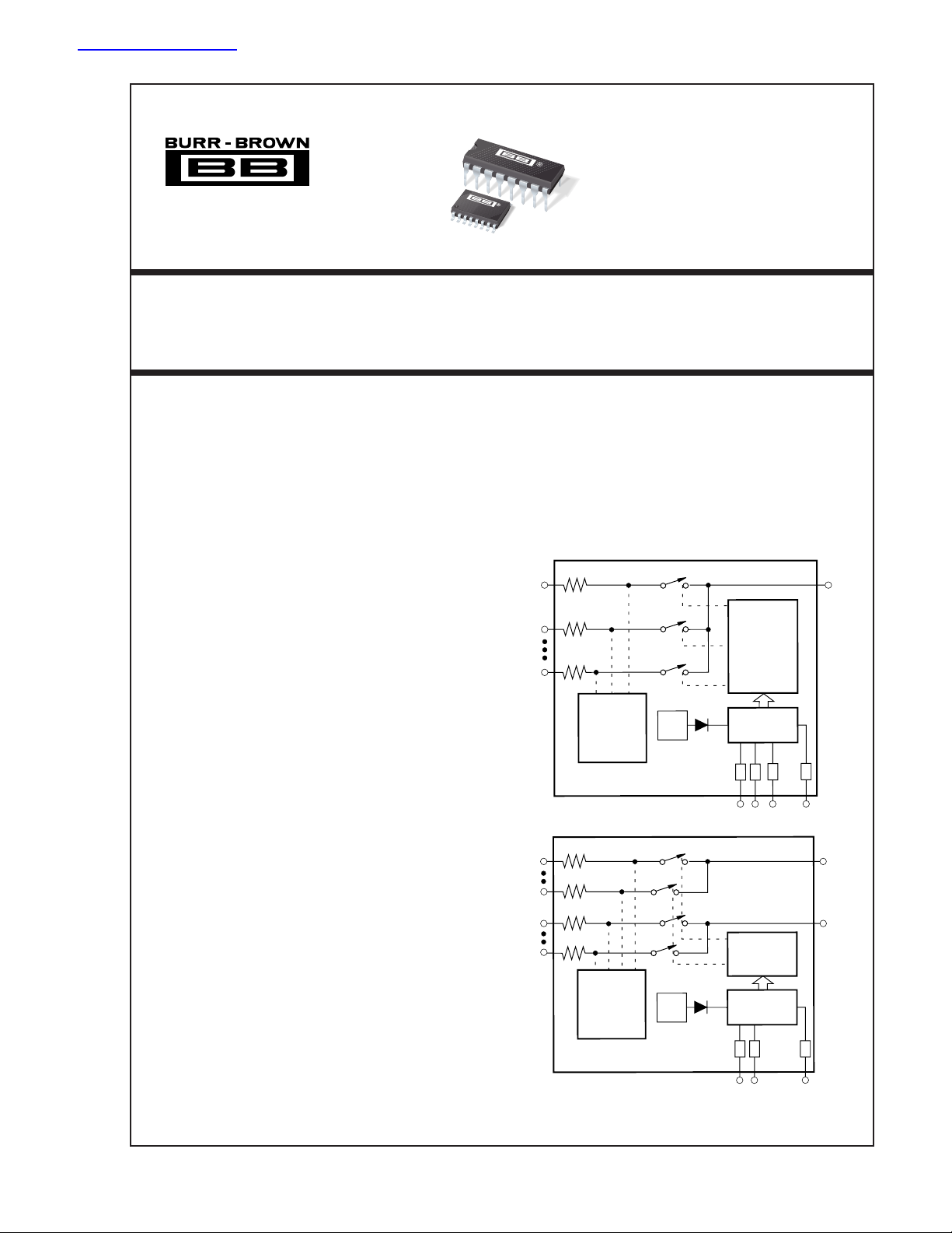
查询MPC508供应商
®
MPC508
MPC509
MPC508A
MPC509A
Single-Ended 8-Channel/Differential 4-Channel
CMOS ANALOG MUL TIPLEXERS
FEA TURES
● ANALOG OVERVOLTAGE PROTECTION:
70Vp-p
● NO CHANNEL INTERACTION DURING
OVERVOLTAGE
● BREAK-BEFORE-MAKE SWITCHING
● ANALOG SIGNAL RANGE:
±15V
● STANDBY POWER: 7.5mW typ
● TRUE SECOND SOURCE
DESCRIPTION
The MPC508A is an 8-channel single-ended analog
multiplexer and the MPC509A is a 4-channel differential multiplexer.
The MPC508A and MPC509A multiplexers have input overvoltage protection. Analog input voltages may
exceed either power supply voltage without damaging
the device or disturbing the signal path of other channels. The protection circuitry assures that signal fidelity is maintained even under fault conditions that
would destroy other multiplexers. Analog inputs can
withstand 70Vp-p signal levels and standard ESD
tests. Signal sources are protected from short circuits
should multiplexer power loss occur; each input presents a 1kΩ resistance under this condition. Digital
inputs can also sustain continuous faults up to 4V
greater than either supply voltage.
These features make the MPC508A and MPC509A
ideal for use in systems where the analog signals
originate from external equipment or separately powered sources.
The MPC508A and MPC509A are fabricated with
Burr-Brown’s dielectrically isolated CMOS technology. The multiplexers are available in plastic DIP and
plastic SOIC packages. Temperature range is –40°C to
+85°C.
FUNCTIONAL DIAGRAMS
1kΩ
In 1
1kΩ
In 2
In 8
In 1A
In 4A
In 1B
In 4B
1kΩ
Overvoltage
Clamp and
Isolation
NOTE: (1) Digital
Input Protection.
MPC508A
1kΩ
1kΩ
1kΩ
1kΩ
Overvoltage
Clamp and
Isolation
NOTE: (1) Digital
Input Protection.
MPC509A
Signal
Signal
5V
Ref
5V
Ref
Decoder/
Driver
Level
Shift
(1)
(1)
(1)
A
A
A
2
1
0
Decoder/
Driver
Level
Shift
(1) (1) (1)
A
A
1
0
Out
(1)
EN
Out A
Out B
EN
International Airport Industrial Park • Mailing Address: PO Box 11400, Tucson, AZ 85734 • Street Address: 6730 S. Tucson Blvd., Tucson, AZ 85706 • Tel: (520) 746-1111 • Twx: 910-952-1111
Internet: http://www.burr-brown.com/ • FAXLine: (800) 548-6133 (US/Canada Only) • Cable: BBRCORP • Telex: 066-6491 • FAX: (520) 889-1510 • Immediate Product Info: (800) 548-6132
©
1988 Burr-Brown Corporation PDS-775E Printed in U.S.A. March, 1998
1
MPC508A, 509A
®
Page 2
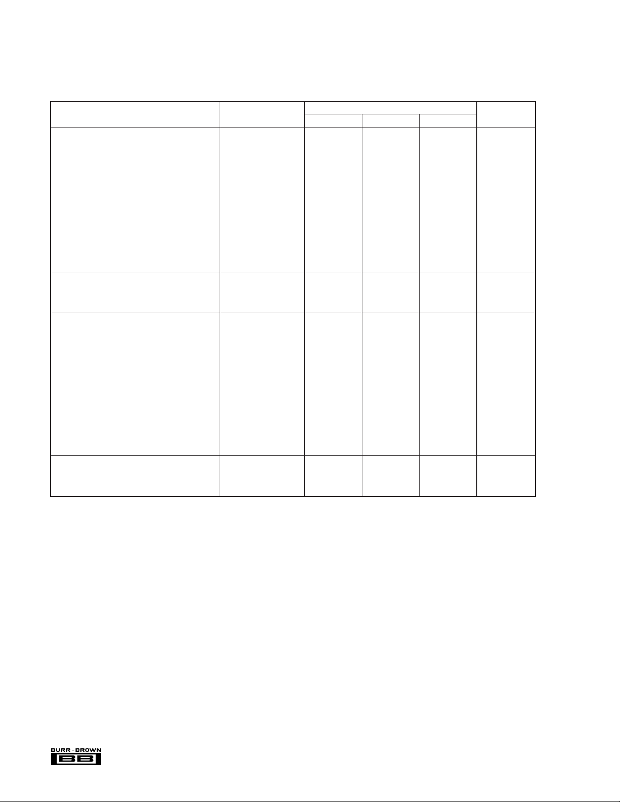
SPECIFICATIONS
ELECTRICAL
Supplies = +15V, –15V; VAH (Logic Level High) = +4.0V, VAL (Logic Level Low) = +0.8V, unless otherwise specified.
MPC508A/509A
PARAMETER TEMP MIN TYP MAX UNITS
ANALOG CHANNEL CHARACTERISTICS
, Analog Signal Range Full –15 +15 V
V
S
R
, On Resistance
ON
I
(OFF), Off Input Leakage Current +25°C 0.5 nA
S
I
(OFF), Off Output Leakage Current +25°C 0.2 nA
D
MPC508A Full 5 nA
MPC509A Full 5 nA
I
(OFF) with Input Overvoltage Applied
D
I
(ON), On Channel Leakage Current +25°C2nA
D
MPC508A Full 10 nA
MPC509A Full 10 nA
I
Differential Off Output Leakage Current
DIFF
(MPC509A Only) Full 10 nA
DIGITAL INPUT CHARACTERISTICS
V
, Input Low Threshold Drive Full 0.8 V
AL
V
, Input High Threshold
AH
I
, Input Leakage Current (High or Low)
A
SWITCHING CHARACTERISTICS
t
, Access Time +25°C 0.5 µs
A
t
, Break-Before-Make Delay +25°C2580 ns
OPEN
t
(EN), Enable Delay (ON) +25°C 200 ns
ON
t
(EN), Enable Delay (OFF) +25°C 250 ns
OFF
Settling Time (0.1%) +25°C 1.2 µs
"OFF Isolation"
C
(OFF), Channel Input Capacitance +25°C5pF
S
C
(OFF), Channel Output Capacitance: MPC508A +25°C25pF
D
MPC509A +25°C12pF
C
, Digital Input Capacitance 25°C5pF
A
C
(OFF), Input to Output Capacitance +25°C 0.1 pF
DS
POWER REQUIREMENTS
P
, Power Dissipation Full 7.5 mW
D
I+, Current Pin 1
I–, Current Pin 27
(1)
+25°C 1.3 1.5 kΩ
Full 1.5 1.8 kΩ
Full 10 nA
(2)
+25°C 4.0 nA
Full µA
(3)
(4)
Full 4.0 V
Full 1.0 µA
Full 0.6 µs
Full 500 ns
Full 500 ns
(0.01%) +25°C 3.5 µs
(5)
(6)
(6)
+25°C5068 dB
Full 0.7 1.5 mA
Full 5 20 µA
NOTES: (1) V
(4) Digital input leakage is primarily due to the clamp diodes. Typical leakage is less than 1nA at 25°C. (5) V
Worst-case isolation occurs on channel 4 due to proximity of the output pins. (6) V
OUT
= ±10V, I
= –100µA. (2) Analog overvoltage = ±33V. (3) To drive from DTL/TTL circuits. 1kΩ pull-up resistors to +5.0V supply are recommended.
OUT
, VA = 0V or 4.0V.
EN
= 0.8V, RL = 1kΩ, CL = 15pF, VS = 7Vrms, f = 100kHz.
EN
The information provided herein is believed to be reliable; however, BURR-BROWN assumes no responsibility for inaccuracies or omissions. BURR-BROWN
assumes no responsibility for the use of this information, and all use of such information shall be entirely at the user’s own risk. Prices and specifications are subject
to change without notice. No patent rights or licenses to any of the circuits described herein are implied or granted to any third party. BURR-BROWN does not
authorize or warrant any BURR-BROWN product for use in life support devices and/or systems.
®
MPC508A, 509A
2
Page 3
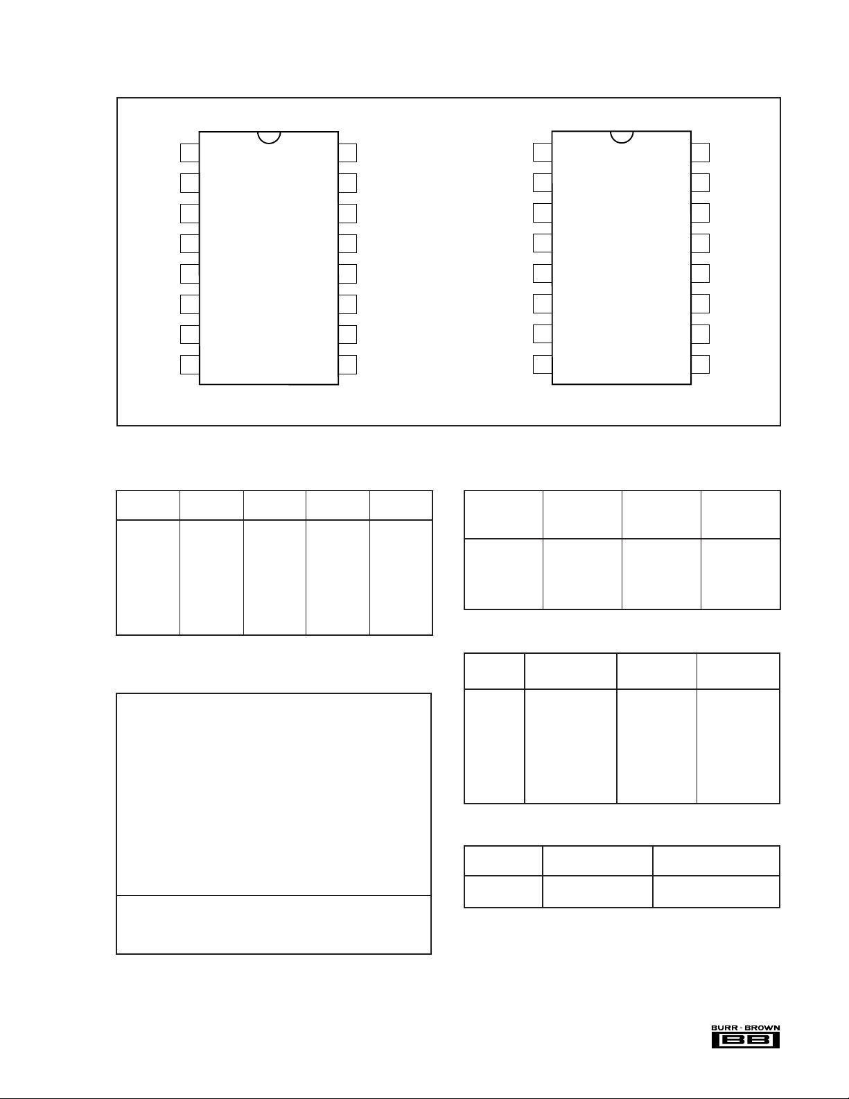
PIN CONFIGURATIONS
Top View
A
16
15
14
13
12
11
10
9
1
A
2
Ground
+V
SUPPLY
In 5
In 6
In 7
In 8
–V
En
SUPPLY
In 1
In 2
In 3
In 4
Out
1
A
0
2
3
4
5
6
7
8
MPC508A (Plastic)
TRUTH TABLES
MPC508A
A
2
X X X L None
LLLH1
LLHH2
LHLH3
LHHH4
HLLH5
HLHH6
HHLH7
HHHH8
A
1
A
0
EN CHANNEL
"ON"
Top View
A
16
15
14
13
12
11
10
9
1
Ground
+V
SUPPLY
In 1B
In 2B
In 3B
In 4B
Out B
–V
En
SUPPLY
In 1A
In 2A
In 3A
In 4A
Out A
1
A
0
2
3
4
5
6
7
8
MPC509 A (Plastic)
MPC509A
CHANNEL
A
1
A
0
EN PAIR
X X L None
LLH1
LHH 2
HLH 3
HHH 4
ORDERING INFORMATION
"ON"
ABSOLUTE MAXIMUM RATINGS
(1)
Voltage between supply pins ...............................................................44V
V+ to ground ........................................................................................ 22V
V– to ground ........................................................................................ 25V
Digital input overvoltage V
Analog input overvoltage V
Continuous current, S or D ............................................................... 20mA
, VA:
EN
V
(+) ................................................... +4V
SUPPLY
V
(–).................................................... –4V
SUPPLY
or 20mA, whichever occurs first.
:
S
V
(+) ................................................ +20V
SUPPLY
V
(–).................................................–20V
SUPPLY
Peak current, S or D
(pulsed at 1ms, 10% duty cycle max) ............................................ 40mA
Power dissipation
(2)
.......................................................................... 1.28W
Operating temperature range............................................ –40°C to +85°C
Storage temperature range ............................................. –65°C to +150°C
NOTE: (1) Absolute maximum ratings are limiting values, applied individually, beyond which the serviceability of the circuit may be impaired. Functional operation under any of these conditions is not necessarily implied.
(2) Derate 1.28mW/°C above T
= +70°C.
A
PRODUCT PACKAGE RANGE DESCRIPTION
TEMPERATURE
MPC508AP 16-Pin Plastic DIP –40°C to +85°C 8-Channel
Single-Ended
MPC508AU 16-Pin Plastic SOIC –40°C to +85°C 8-Channel
Single-Ended
MPC509AP 16-Pin Plastic DIP –40°C to +85°C 4-Channel
Differential
MPC509AU 16-Pin Plastic SOIC –40°C to +85°C 4-Channel
Differential
PACKAGE INFORMATION
PRODUCT PACKAGE NUMBER
MPC508/509AP 16-Pin Plastic DIP 180
MPC508/509AU 16-Pin Plastic SOIC 211
NOTE: (1) For detailed drawing and dimension table, please see end of data
sheet, or Appendix C of Burr-Brown IC Data Book.
3
MPC508A, 509A
PACKAGE DRAWING
(1)
®
Page 4
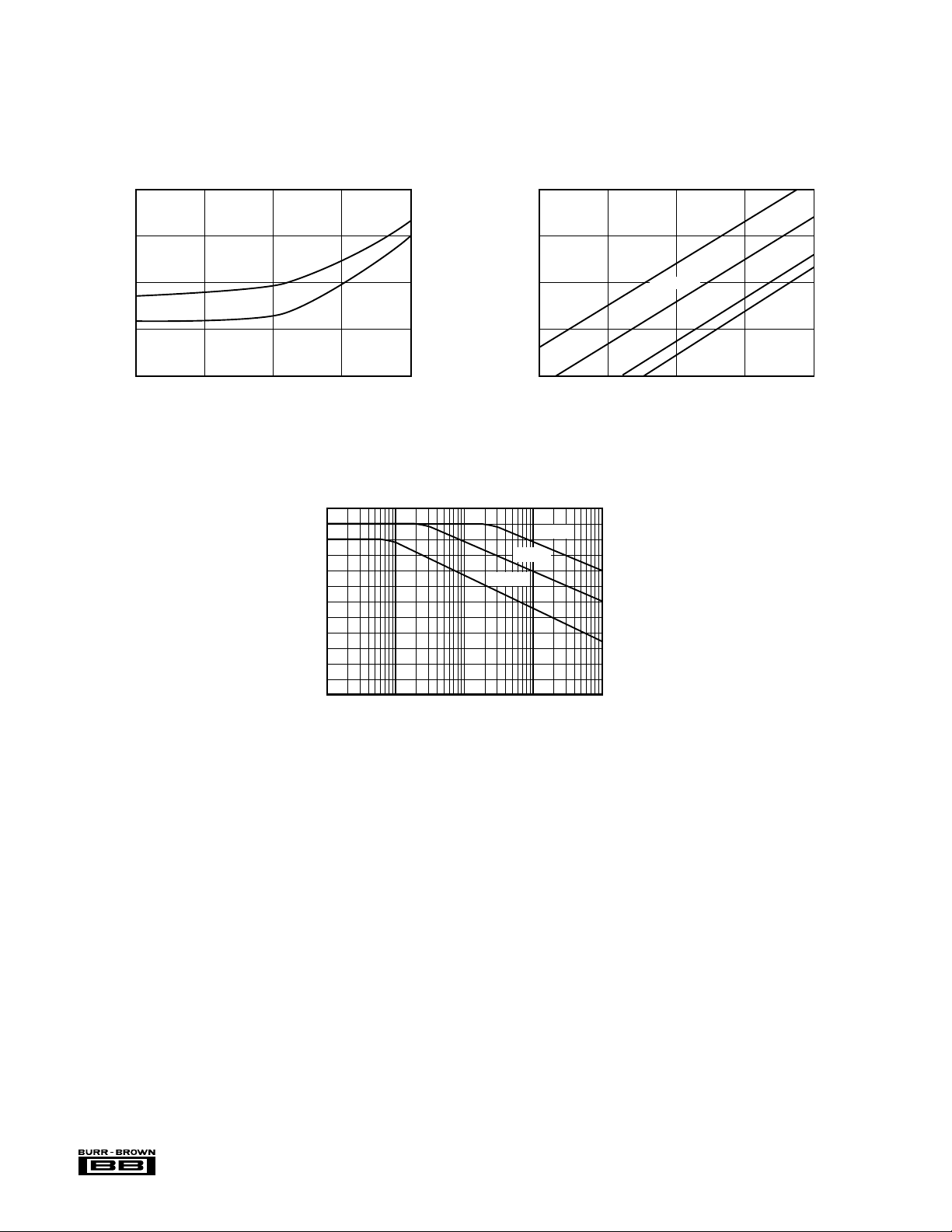
TYPICAL PERFORMANCE CURVES
Typical at +25°C, unless otherwise noted.
SOURCE RESISTANCE FOR 20V STEP CHANGE
1k
100
10
Settling Time (µs)
1
0.1
0.01 0.1
SETTLING TIME vs
To ±0.01%
To ±0.1%
1
Source Resistance (kΩ)
120
100
80
60
10 100
COMBINED CMR vs
FREQUENCY MPC509A AND INA110
1
CROSSTALK vs SIGNAL FREQUENCY
0.1
Rs = 100kΩ
0.01
0.001
Crosstalk (% of Off Channel Signal)
0.0001
110
Signal Frequency (Hz)
G = 500
G = 100
G = 10
Rs = 10kΩ
R
100
= 1kΩ
s
= 100Ω
R
s
1k 10k
40
20
Common-Mode Rejection (dB)
0
1 10 100 1k 10k
Frequency (Hz)
®
MPC508A, 509A
4
Page 5

DISCUSSION OF
Z
L
R
S4A
R
S48
R
OFF4A
R
OFF4B
C
CM
R
S1
R
S1B
R
ON1A
R
ON1B
I
L
Cd/2
Cd/2
R
CM
Rd/2
Rd/2
I
BIAS A
I
BIAS B
R
CM4
R
CM1
V
S1
V
S8
I
LB
PERFORMANCE
DC CHARACTERISTICS
The static or dc transfer accuracy of transmitting the multiplexer input voltage to the output depends on the channel ON
resistance (R
the load bias current and the multiplexer leakage current.
Single-Ended Multiplexer Static Accuracy
The major contributors to static transfer accuracy for singleended multiplexers are:
Source resistance loading error;
Multiplexer ON resistance error;
and, DC offset error caused by both load bias current and
multiplexer leakage current.
Resistive Loading Errors
The source and load impedances will determine the input
resistive loading errors. To minimize these errors:
• Keep loading impedance as high as possible. This
minimizes the resistive loading effects of the source
resistance and multiplexer ON resistance. As a guideline,
load impedances of 108Ω, or greater, will keep resistive
loading errors to 0.002% or less for 1000Ω source impedances. A 106Ω load impedance will increase source
loading error to 0.2% or more.
• Use sources with impedances as low as possible. 1000Ω
source resistance will present less than 0.001% loading
error and 10kΩ source resistance will increase source
loading error to 0.01% with a 10
Input resistive loading errors are determined by the following
relationship (see Figure 1).
Source and Multiplexer Resistive Loading Error
where RS = source resistance
R
R
), the load impedance, the source impedance,
ON
8
load impedance.
R
+R
S
∈ RS+R
()
= load resistance
L
= multiplexer ON resistance
ON
ON
=
RS+ RON+ R
ON
x 100%
L
Differential Multiplexer Static Accuracy
Static accuracy errors in a differential multiplexer are difficult to control, especially when it is used for multiplexing
low-level signals with full-scale ranges of 10mV to 100mV.
The matching properties of the multiplexer, source and
output load play a very important part in determining the
transfer accuracy of the multiplexer. The source impedance
unbalance, common-mode impedance, load bias current mismatch, load differential impedance mismatch, and commonmode impedance of the load all contribute errors to the
multiplexer. The multiplexer ON resistance mismatch, leakage current mismatch and ON resistance also contribute to
differential errors.
The effects of these errors can be minimized by following the
general guidelines described in this section, especially for
low-level multiplexing applications. Refer to Figure 2.
Load (Output Device) Characteristics
• Use devices with very low bias current. Generally, FET
input amplifiers should be used for low-level signals less
than 50mV FSR. Low bias current bipolar input amplifiers are acceptable for signal ranges higher than 50mV
FSR. Bias current matching will determine the input
offset.
• The system dc common-mode rejection (CMR) can never
be better than the combined CMR of the multiplexer and
driven load. System CMR will be less than the device
which has the lower CMR figure.
• Load impedances, differential and common-mode, should
10
Ω or higher.
be 10
I
R
S1
V
S1
R
S8
V
S8
R
ON
R
OFF
BIAS
V
M
I
L
Z
L
Measured
Voltage
FIGURE 1. MPC508A DC Accuracy Equivalent Circuit.
Input Offset Voltage
Bias current generates an input OFFSET voltage as a result
of the IR drop across the multiplexer ON resistance and
source resistance. A load bias current of 10nA will generate
an offset voltage of 20µV if a 1kΩ source is used. In general,
for the MPC508A, the OFFSET voltage at the output is
determined by:
where I
I
= Multiplexer leakage current
L
R
ON
R
S
V
= Bias current of device multiplexer is driving
B
= Multiplexer ON resistance
= source resistance
= (IB + IL) (RON + RS)
OFFSET
FIGURE 2. MPC509A DC Accuracy Equivalent Circuit.
5
MPC508A, 509A
®
Page 6

Source Characteristics
• The source impedance unbalance will produce offset,
common-mode and channel-to-channel gain-scatter errors. Use sources which do not have large impedance
unbalances if at all possible.
• Keep source impedances as low as possible to minimize
resistive loading errors.
• Minimize ground loops. If signal lines are shielded,
ground all shields to a common point at the system
analog common.
If the MPC509A is used for multiplexing high-level signals
of ±1V to ±10V full-scale ranges, the foregoing precautions
should still be taken, but the parameters are not as critical as
for low-level signal applications.
DYNAMIC CHARACTERISTICS
Settling Time
The gate-to-source and gate-to-drain capacitance of the CMOS
FET switches, the RC time constants of the source and the
load determine the settling time of the multiplexer.
Governed by the charge transfer relation i = C (dV/dt), the
charge currents transferred to both load and source by the
analog switches are determined by the amplitude and rise
time of the signal driving the CMOS FET switches and the
gate-to-drain and gate-to-source junction capacitances as
shown in Figures 3 and 4. Using this relationship, one can see
that the amplitude of the switching transients, seen at the
source and load, decrease proportionally as the capacitance
of the load and source increase. The trade-off for reduced
switching transient amplitude is increased settling time. In
effect, the amplitude of the transients seen at the source and
load are:
= (i/C) dt
dV
L
where i = C (dV/dt) of the CMOS FET switches
C = load or source capacitance
The source must then redistribute this charge, and the effect
of source resistance on settling time is shown in the Typical
Performance Curves. This graph shows the settling time for
a 20V step change on the input. The settling time for smaller
step changes on the input will be less than that shown in the
curve.
MPC508A Channel
Source
R
S
Node A
C
S
Load
C
L
R
L
R
SA
C
R
CMS
C
CMS
R
SA
Source
C
SB
SB
Node A
MPC509A
Channel
Rd
Load
Rd
Node B
Cd
Cd
A
Z
CM
B
A
B
FIGURE 4. Settling and Common-Mode-Effects—
MPC509A
Switching Time
This is the time required for the CMOS FET to turn ON after
a new digital code has been applied to the Channel Address
inputs. It is measured from the 50 percent point of the address
input signal to the 90 percent point of the analog signal seen
at the output for a 10V signal change between channels.
Crosstalk
Crosstalk is the amount of signal feedthrough from the three
(MPC509A) or seven (MPC508A) OFF channels appearing
at the multiplexer output. Crosstalk is caused by the voltage
divider effect of the OFF channel, OFF resistance and junction capacitances in series with the R
and RS impedances
ON
of the ON channel. Crosstalk is measured with a 20Vp-p
1kHz sine wave applied to all OFF channels. The crosstalk
for these multiplexers is shown in the Typical Performance
Curves.
Common-Mode Rejection (MPC509A Only)
The matching properties of the load, multiplexer and source
affect the common-mode rejection (CMR) capability of a
differentially multiplexed system. CMR is the ability of the
multiplexer and input amplifier to reject signals that are
common to both inputs, and to pass on only the signal
difference to the output. For the MPC509A, protection is
provided for common-mode signals of ±20V above the
power supply voltages with no damage to the analog switches.
The CMR of the MPC509A and Burr-Brown’s INA110
instrumentation amplifier is 110dB at DC to 10Hz (G = 100)
with a 6dB/octave roll off to 70dB at 1000Hz. This measurement of CMR is shown in the Typical Performance Curves
and is made with a Burr-Brown model INA110 instrumentation amplifier connected for gains of 10, 100, and 500.
FIGURE 3. Settling Time Effects—MPC508A
®
MPC508A, 509A
6
Page 7

Factors which will degrade multiplexer and system DC CMR
are:
• Amplifier bias current and differential impedance mismatch
• Load impedance mismatch
• Multiplexer impedance and leakage current mismatch
• Load and source common-mode impedance
SWITCHING WAVEFORMS
TYPICAL AT +25°C UNLESS OTHERWISE NOTED.
AC CMR roll off is determined by the amount of commonmode capacitances (absolute and mismatch) from each signal
line to ground. Larger capacitances will limit CMR at higher
frequencies; thus, if good CMR is desired at higher
frequencies, the common-mode capacitances and unbalance
of signal lines and multiplexer-to-amplifier wiring must be
minimized. Use twisted-shielded-pair signal lines wherever
possible.
BREAK-BEFORE-MAKE DELAY (t
4.0V
V
AM
Address Drive
)
(V
0V
50% 50%
t
OPEN
ENABLE DELAY (t
Enable Drive
V
4.0V
AM
90%
t
(EN)
ON
Output
ON
(EN), t
t
OFF
A
OFF
50%
(EN)
(EN))
OPEN
V
0V
Output
90%
)
In 2 Thru In 7
GND
MPC508A
2
1
In 2 Thru In 8
0
GND
(1)
In 1
In 8
Out
(1)
MPC508A
A
50Ω
+4.0V
A
A
En
50Ω
2
1
0
A
A
A
En
A
NOTE: (1) Similar connection for MPC509A.
V
A
1kΩ
In 1
Out
1kΩ
+10V
+5V
V
OUT
12.5pF
12.5pF
VA Input
2V/Div
1 On
Output
0.5V/Div
100ns/Div
Enable Drive
2V/Div
Output
2V/Div
NOTE: (1) Similar connection for MPC509A.
7
100ns/Div
®
MPC508A, 509A
Page 8

PERFORMANCE CHARACTERISTICS AND TEST CIRCUITS
Unless otherwise specified: TA = +25, VS = ±15V, VAM = +4V, VAL = 0.8V.
ON RESISTANCE vs ANALOG INPUT SIGNAL,
SUPPLY VOLTAGE
ON RESISTANCE vs
ANALOG INPUT VOLTAGE
1.4
1.3
TA = +125°C
1.2
1.1
1.0
0.9
0.8
On Resistance (kΩ)
TA = +25°C
TA = –55°C
0.7
0.6
–10–8–6–4–20246810
Analog Input (V)
RON = V2/100µA
100µA
V
2
In
Out
V
IN
NORMALIZED ON RESISTANCE
vs SUPPLY VOLTAGE
1.6
1.5
1.4
±125°C > TA > –55°C
= +5V
V
IN
1.3
1.2
1.1
1.0
Normalized On Resistance
(Referred to Value at ±15V)
0.9
0.8
±5 ±6 ±7 ±8 ±9 ±10 ±11 ±12 ±13 ±14 ±15
Supply Voltage (V)
SUPPLY CURRENT vs TOGGLE FREQUENCY
+15V/+10V
+I
A
MPC508A
A
2
V
A
50Ω
+4V
En
A
1
A
0
GND
(1)
En
In 2 Thru In 7
In 8
Out
–V
A
–I
±10V/±5V
SUPPLY
–15V/–10V
NOTE: (1) Similar connection for MPC509A.
SUPPLY
±10V/±5V
±10V/±5V
10MΩ
14pF
8
6
4
Supply Current (mA)
2
VS = ±15V
VS = ±10V
0
100 1k 10k 100k 1M 10M
Toggle Frequency (Hz)
®
MPC508A, 509A
8
Page 9

PERFORMANCE CHARACTERISTICS AND TEST CIRCUITS (CONT)
LEAKAGE CURRENT vs TEMPERATURE
En
+0.8V
Out
A
(Off)
I
±10V
D
±
10V
±
10V
Out
IS (Off)
A
±10V
±
10V
En
+0.8V
NOTE: (1) Two measurements per channel: +10V/–10V and –10V/+10V.
(Two measurements per device for I
(Off): +10V/–10V and –10V/+10V).
D
ANALOG INPUT OVERVOLTAGE CHARACTERISTICS
A
0
Out
A
En
A
1
+4.0V
100nA
10nA
1nA
Leakage Current
100pA
10pA
25 50 75 100 125
21
18
I
D
±10V
(On)
On Leakage
Current I
(On)
D
Temperature (°C)
Off Output
Current
(Off)
I
D
Leakage Current
Off Input
(Off)
I
S
7
6
I
IN
A
±V
IN
IO (Off)
A
15
12
9
6
Analog Input Current (mA)
3
Analog Input
Current (I
IN
)
Output Off
Leakage Current
(Off)
I
O
0
5
4
3
2
1
Output Off Leakage Current (nA)
0
±12 ±15 ±18 ±21 ±24 ±27 ±30 ±33 ±36
Analog Input Overvoltage (V)
®
9
MPC508A, 509A
Page 10

PERFORMANCE CHARACTERISTICS AND TEST CIRCUITS (CONT)
g
)
ACCESS TIME vs LOGIC LEVEL (High)
V
REF
A
2
V
A
50Ω
+4V
En
A
1
MPC
A
0
508A
GND
NOTE: (1) Similar connection for MPC509A.
ACCESS TIME WAVEFORM
VAM
4.0V
50%
10V
90%
t
A
+15V
+V
In 1
In 2 Thru
In 7
(1)
In 8
Out
–V
–15V
Output A
10V
Address
Drive (V
0V
–10V
+10V
)
A
10MΩ
Probe
14pF
1000
900
800
700
600
Access Time (ns)
500
400
300
3456789101112131415
Lo
ic Level High (V
VA Input
2V/Div
Output A
5V/Div
ON-CHANNEL CURRENT vs VOLTAGE
±V
IN
200ns/Div
±14
±12
±10
–55°C
+25°C
+125°C
±8
A
±6
±4
Switch Current (mA)
±2
0
0 ±2 ±4 ±6 ±8 ±10 ±12 ±14 ±16
VIN –Voltage Across Switch (V)
®
MPC508A, 509A
10
Page 11

Direct
Multiplexer
Output
Buffered
OPA602
1/4 OPA404
MPC508A
Out
Out
In 1
In 2
In 3
In 8
A
0A1A2
2
8
A
0A1A2
MPC508A
8
2
6-Bit Channel
Address Generator
A0A1A
2
In 1
In 2
In 3
In 8
In 1
In 8
MPC508A
En
En
Out
En
+V
+V
+V
4LSBs 4MSBs
8 Analog Inputs (CH57 to 64) 8 Analog Inputs (CH1 to 8)
Settling Time to
±0.01% is 20µs
with R
S
= 100Ω
µ
INSTALLATION AND
OPERATING INSTRUCTIONS
The ENABLE input, pin 2, is included for expansion of the
number of channels on a single node as illustrated in Figure
5. With ENABLE line at a logic 1, the channel is selected by
the 2-bit (MPC509A) or 3-bit (MPC508A) Channel Select
Address (shown in the Truth Tables). If ENABLE is at logic
0, all channels are turned OFF, even if the Channel Address
Lines are active. If the ENABLE line is not to be used, simply
tie it to +V
If the +15V and/or –15V supply voltage is absent or shorted
to ground, the MPC509A and MPC508A multiplexers will
not be damaged; however, some signal feedthrough to the
output will occur. Total package power dissipation must not
be exceeded.
For best settling speed, the input wiring and interconnections
between multiplexer output and driven devices should be
kept as short as possible. When driving the digital inputs
from TTL, open collector output with pull-up resistors are
recommended.
To preserve common-mode rejection of the MPC509A, use
twisted-shielded pair wire for signal lines and inter-tier
connections and/or multiplexer output lines. This will help
common-mode capacitance balance and reduce stray signal
pickup. If shields are used, all shields should be connected as
close as possible to system analog common or to the common-mode guard driver.
CHANNEL EXPANSION
Single-Ended Multiplexer (MPC508A)
Up to 32 channels (four multiplexers) can be connected to a
single node, or up to 64 channels using nine MPC508A
multiplexers on a two-tiered structure as shown in Figures 5
and 6.
In 1
In 2
In 3
Group 1
In 8
8 Analog Inputs8 Analog Inputs
In 1
In 2
In 3
In 8
FIGURE 5. 32-Channel, Single-Tier Expansion.
SUPPLY
MPC
508A
Ch1-8
A
2A1A0
A
2A1A0
MPC
508A
Group 4
Ch25-42
.
8
2
2
8
Out
Group 1
Enable
5-Bit
Binary
0
2
Counter
1
2
2
2
3
2
2
Group 4
Enable
Out
1 of 4
4
Decoder
Settling Time to 0.01% for RS < 100Ω
—Two MPC508A units in parallels: 10µs
—Four MPC509 A units in parallels: 12
Multiplexer
Output
To
Group
2
To
Group
3
Direct
Buffered
OPA602
1/4 OPA404
s
FIGURE 6. Channel Expansion Up to 64 Channels Using
8 x 8 Two-Tiered Expansion.
Differential Multiplexer (MPC509A)
Single or multitiered configurations can be used to expand
multiplexer channel capacity up to 32 channels using a
32 x 1 or 16 channels using a 4 x 4 configuration.
Single-Node Expansion
The 32 x 1 configuration is simply eight (MPC509A) units
tied to a single node. Programming is accomplished with a
5-bit counter, using the 2LSBs of the counter to control
Channel Address inputs A
and A1 and the 3MSBs of the
0
counter to drive a 1-of-8 decoder. The 1-of-8 decoder then is
used to drive the ENABLE inputs (pin 2) of the MPC509A
multiplexers.
Two-Tier Expansion
Using a 4 x 4 two-tier structure for expansion to 16 channels,
the programming is simplified. A 4-bit counter output does
not require a 1-of-8 decoder. The 2LSBs of the counter drive
the A
and A1 inputs of the four first-tier multiplexers and the
0
2MSBs of the counter are applied to the A
and A1 inputs of
0
the second-tier multiplexer.
Single vs Multitiered Channel Expansion
In addition to reducing programming complexity, two-tier
configuration offers the added advantages over single-node
expansion of reduced OFF channel current leakage (reduced
OFFSET), better CMR, and a more reliable configuration if
a channel should fail in the ON condition (short). Should a
channel fail ON in the single-node configuration, data cannot
be taken from any channel, whereas only one channel group
is failed (4 or 8) in the multitiered configuration.
11
MPC508A, 509A
®
 Loading...