

Page 1
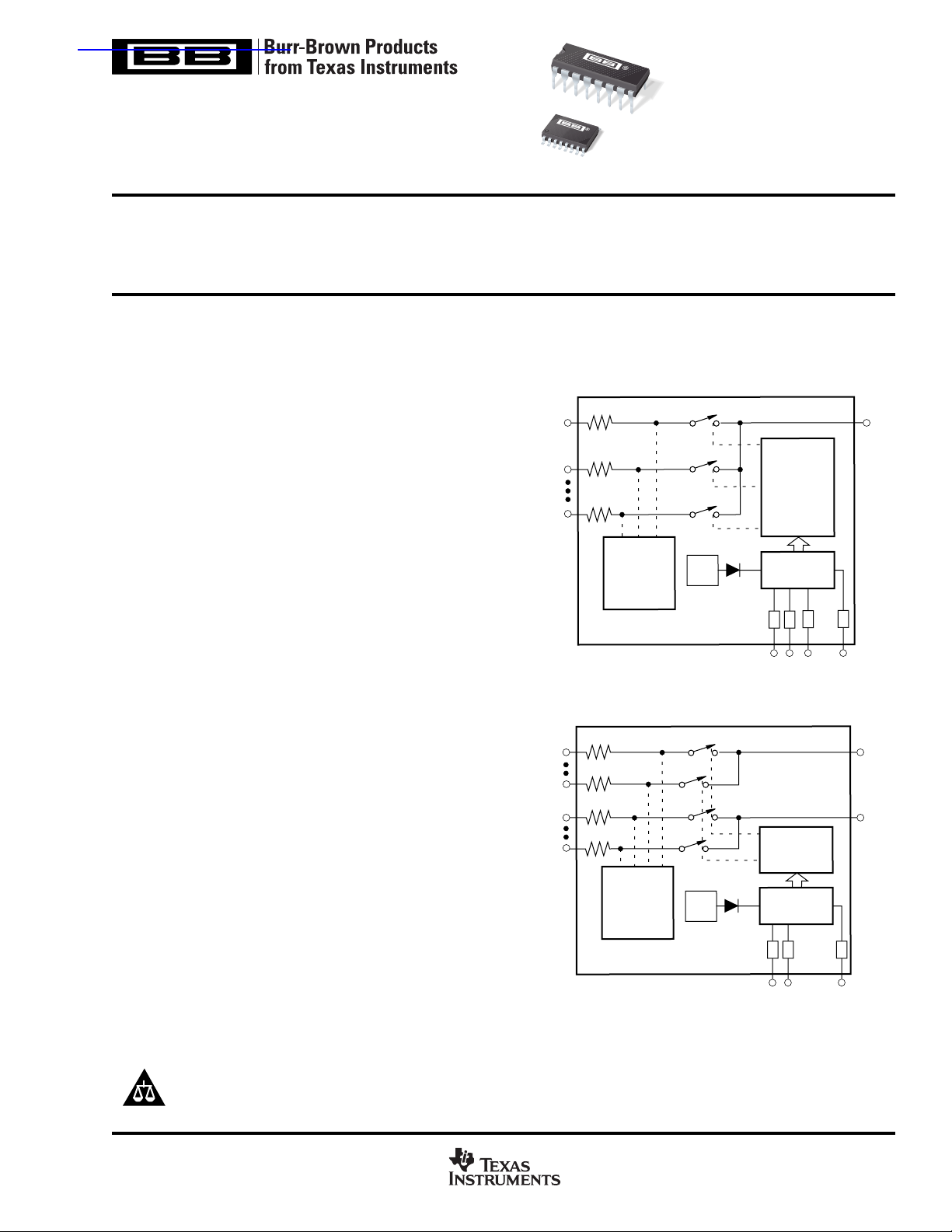
Level
Shift
1kΩ
1kΩ
1kΩ
Overvoltage
Clamp and
Signal
Isolation
5V
Ref
Decoder/
Driver
NOTE: (1) Digital
Input Protection.
In 1
In 2
In 8
MPC508A
A
0
A
1
A
2
EN
(1)
Out
(1)
(1)
(1)
查询MPC509AU/1K供应商
Single-Ended 8-Channel/Differential 4-Channel
CMOS ANALOG MULTIPLEXERS
M
P
C508
MPC508A
MPC509A
M
PC509
SBFS019A – JANUARY 1988 — REVISED OCTOBER 2003
FEATURES
● ANALOG OVERVOLTAGE PROTECTION: 70V
● NO CHANNEL INTERACTION DURING
OVERVOLTAGE
● BREAK-BEFORE-MAKE SWITCHING
● ANALOG SIGNAL RANGE:
±15V
● STANDBY POWER: 7.5mW typ
● TRUE SECOND SOURCE
DESCRIPTION
The MPC508A is an 8-channel single-ended analog
multiplexer and the MPC509A is a 4-channel differential
multiplexer.
The MPC508A and MPC509A multiplexers have input
overvoltage protection. Analog input voltages may exceed
either power supply voltage without damaging the device or
disturbing the signal path of other channels. The protection
circuitry assures that signal fidelity is maintained even under
fault conditions that would destroy other multiplexers. Analog
inputs can withstand 70V
tests. Signal sources are protected from short circuits should
multiplexer power loss occur; each input presents a 1kΩ
resistance under this condition. Digital inputs can also sustain
continuous faults up to 4V greater than either supply voltage.
These features make the MPC508A and MPC509A ideal for
use in systems where the analog signals originate from
external equipment or separately powered sources.
The MPC508A and MPC509A are fabricated with BurrBrown’s dielectrically isolated CMOS technology. The
multiplexers are available in plastic DIP and plastic SOIC
packages. Temperature range is –40°C to +85°C.
Please be aware that an important notice concerning availability, standard warranty, and use in critical applications of
Texas Instruments semiconductor products and disclaimers thereto appears at the end of this data sheet.
All trademarks are the property of their respective owners.
PRODUCTION DATA information is current as of publication date.
Products conform to specifications per the terms of Texas Instruments
standard warranty. Production processing does not necessarily include
testing of all parameters.
signal levels and standard ESD
PP
PP
www.ti.com
In 1A
In 4A
In 1B
In 4B
FUNCTIONAL DIAGRAMS
1kΩ
1kΩ
1kΩ
1kΩ
Overvoltage
Clamp and
Signal
Isolation
NOTE: (1) Digital
Input Protection.
MPC509A
Copyright © 1998-2003, Texas Instruments Incorporated
5V
Ref
Decoder/
Driver
Level
Shift
(1) (1) (1)
A
A
1
0
Out A
Out B
EN
Page 2

ELECTRICAL CHARACTERISTICS
Supplies = +15V, –15V; VAH (Logic Level High) = +4.0V, VAL (Logic Level Low) = +0.8V, unless otherwise specified.
MPC508A/509A
PARAMETER TEMP MIN TYP MAX UNITS
ANALOG CHANNEL CHARACTERISTICS
, Analog Signal Range Full –15 +15 V
V
S
RON, On Resistance
(OFF), Off Input Leakage Current +25°C 0.5 nA
I
S
(OFF), Off Output Leakage Current +25°C 0.2 nA
I
D
MPC508A Full 5 nA
MPC509A Full 5 nA
(OFF) with Input Overvoltage Applied
I
D
(ON), On Channel Leakage Current +25°C2nA
I
D
MPC508A Full 10 nA
MPC509A Full 10 nA
I
Differential Off Output Leakage Current
DIFF
(MPC509A Only) Full 10 nA
DIGITAL INPUT CHARACTERISTICS
, Input Low Threshold Drive Full 0.8 V
V
AL
, Input High Threshold
V
AH
IA, Input Leakage Current (High or Low)
SWITCHING CHARACTERISTICS
, Access Time +25°C 0.5 µs
t
A
, Break-Before-Make Delay +25°C2580 ns
t
OPEN
(EN), Enable Delay (ON) +25°C 200 ns
t
ON
(EN), Enable Delay (OFF) +25°C 250 ns
t
OFF
Settling Time (0.1%) +25°C 1.2 µs
"OFF Isolation"
CS (OFF), Channel Input Capacitance +25°C5pF
(OFF), Channel Output Capacitance: MPC508A +25°C25pF
C
D
MPC509A +25°C12pF
, Digital Input Capacitance 25°C5pF
C
A
CDS (OFF), Input to Output Capacitance +25°C 0.1 pF
POWER REQUIREMENTS
, Power Dissipation Full 7.5 mW
P
D
I+, Current Pin 1
I–, Current Pin 27
NOTES: (1) V
(4) Digital input leakage is primarily due to the clamp diodes. Typical leakage is less than 1nA at 25°C. (5) V
Worst-case isolation occurs on channel 4 due to proximity of the output pins. (6) V
(1)
+25°C 1.3 1.5 kΩ
Full 1.5 1.8 kΩ
Full 10 nA
(2)
(3)
(4)
+25°C 2.0 µA
Full 4.0 V
Full 1.0 µA
Full 0.6 µs
Full 500 ns
Full 500 ns
(0.01%) +25°C 3.5 µs
(5)
= ±10V, I
OUT
(6)
(6)
= –100µA. (2) Analog overvoltage = ±33V. (3) To drive from DTL/TTL circuits. 1kΩ pull-up resistors to +5.0V supply are recommended.
OUT
+25°C5068 dB
Full 0.7 1.5 mA
Full 5 20 µA
= 0.8V, RL = 1kΩ, CL = 15pF, VS = 7Vrms, f = 100kHz.
, VA = 0V or 4.0V.
EN
EN
2
www.ti.com
MPC508A, MPC509A
SBFS019A
Page 3
PIN CONFIGURATIONS
Top View
A
16
15
14
13
12
11
10
9
1
A
2
Ground
+V
SUPPLY
In 5
In 6
In 7
In 8
–V
En
SUPPLY
In 1
In 2
In 3
In 4
Out
1
A
0
2
3
4
5
6
7
8
MPC508A (Plastic)
TRUTH TABLES
MPC508A
A
2
A
1
A
0
EN CHANNEL
X X X L None
LLLH1
LLHH2
LHLH3
LHHH4
HLLH5
HLHH6
HHLH7
HHHH8
"ON"
Top View
A
16
15
14
13
12
11
10
9
1
Ground
+V
SUPPLY
In 1B
In 2B
In 3B
In 4B
Out B
–V
SUPPLY
In 1A
In 2A
In 3A
In 4A
Out A
A
En
1
0
2
3
4
5
6
7
8
MPC509 A (Plastic)
MPC509A
"ON"
CHANNEL
A
1
X X L None
LLH 1
LHH 2
HLH 3
HHH 4
A
0
EN PAIR
ABSOLUTE MAXIMUM RATINGS
(1)
Voltage between supply pins ............................................................... 44V
V+ to ground ........................................................................................ 22V
V– to ground ........................................................................................ 25V
Digital input overvoltage V
Analog input overvoltage V
Continuous current, S or D ............................................................... 20mA
, VA:
EN
V
(+) ................................................... +4V
SUPPLY
V
(–) ................................................... –4V
SUPPLY
or 20mA, whichever occurs first.
:
S
V
(+) ................................................ +20V
SUPPLY
V
(–) ................................................ –20V
SUPPLY
Peak current, S or D
(pulsed at 1ms, 10% duty cycle max) ............................................ 40mA
Power dissipation
(2)
.......................................................................... 1.28W
Operating temperature range ........................................... –40°C to +85°C
Storage temperature range............................................. –65°C to +150°C
NOTE: (1) Absolute maximum ratings are limiting values, applied individually, beyond which the serviceability of the circuit may be impaired. Functional operation under any of these conditions is not necessarily implied.
(2) Derate 1.28mW/°C above T
= +70°C.
A
MPC508A, MPC509A
SBFS019A
PACKAGE/ORDERING INFORMATION
For the most current package and ordering information, see
the Package Option Addendum located at the end of this
data sheet.
www.ti.com
3
Page 4
q
)
g
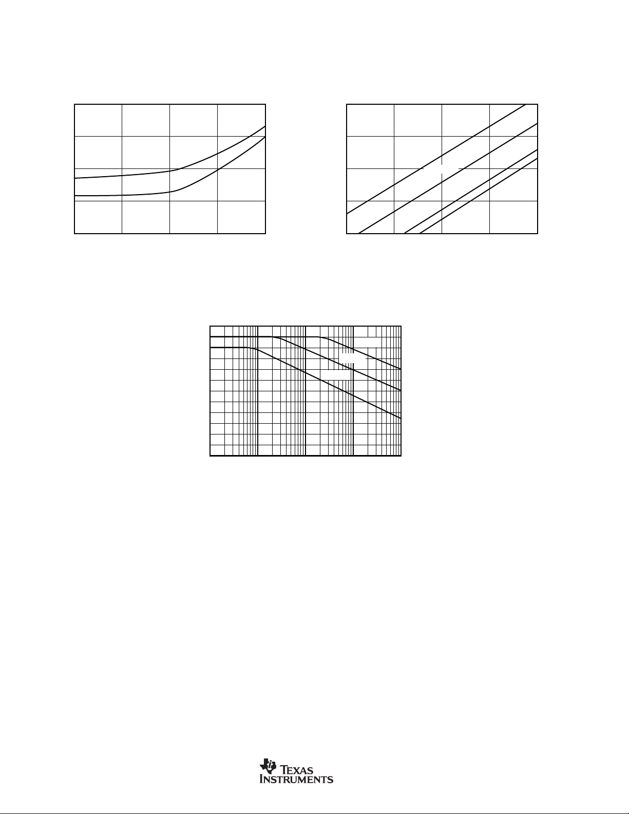
TYPICAL PERFORMANCE CURVES
Typical at +25°C unless otherwise noted.
SOURCE RESISTANCE FOR 20V STEP CHANGE
1k
100
10
Settling Time (µs)
1
0.1
0.01 0.1
SETTLING TIME vs
To ±0.01%
To ±0.1%
1
Source Resistance (kΩ)
120
100
80
60
10 100
COMBINED CMR vs
FREQUENCY MPC509A AND INA110
1
0.1
0.01
0.001
Crosstalk (% of Off Channel Signal)
0.0001
110
G = 100
G = 10
CROSSTALK vs SIGNAL FREQUENCY
Rs = 100kΩ
nal Frequency (Hz)
Si
G = 500
Rs = 10kΩ
R
100
= 1kΩ
s
= 100Ω
R
s
1k 10k
40
20
Common-Mode Rejection (dB)
0
1 10 100 1k 10k
uency (Hz
Fre
4
www.ti.com
MPC508A, MPC509A
SBFS019A
Page 5
DISCUSSION OF
PERFORMANCE
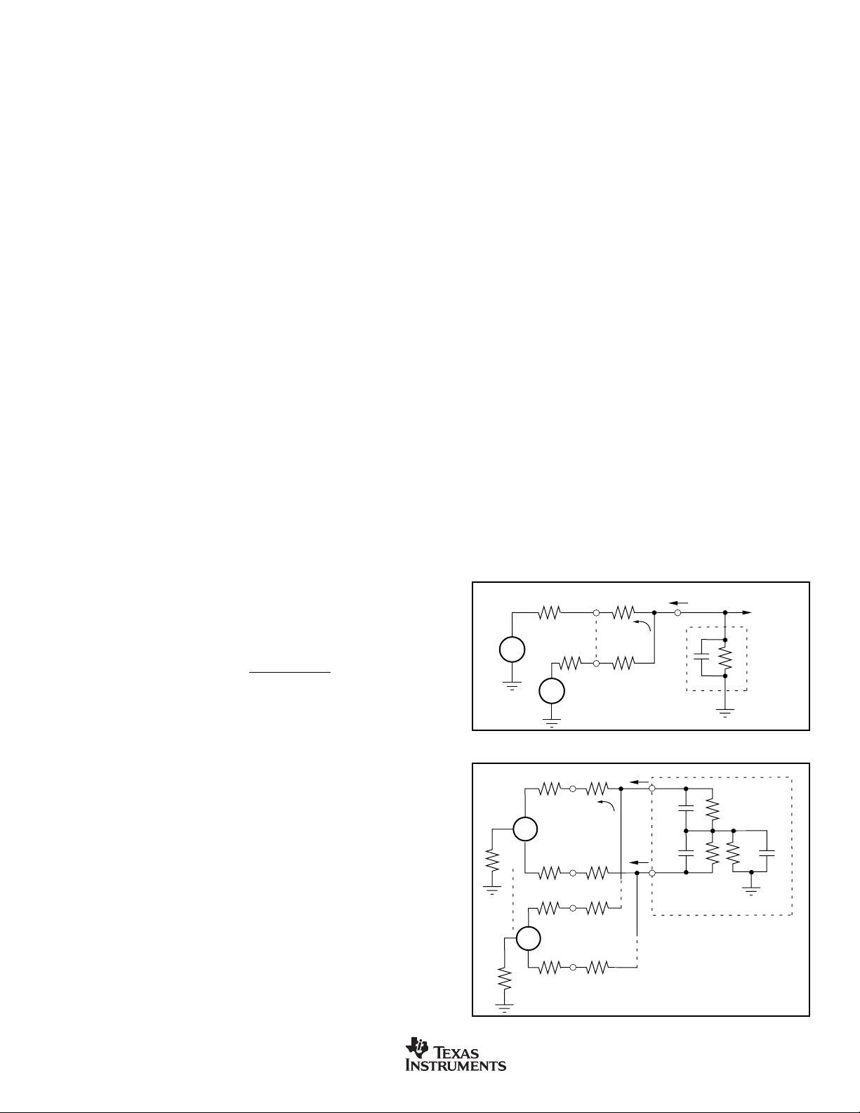
DC CHARACTERISTICS
The static or dc transfer accuracy of transmitting the multiplexer input voltage to the output depends on the channel ON
resistance (RON), the load impedance, the source impedance,
the load bias current and the multiplexer leakage current.
Single-Ended Multiplexer Static Accuracy
The major contributors to static transfer accuracy for singleended multiplexers are:
Source resistance loading error;
Multiplexer ON resistance error;
and, dc offset error caused by both load bias current and
multiplexer leakage current.
Resistive Loading Errors
The source and load impedances will determine the input
resistive loading errors. To minimize these errors:
• Keep loading impedance as high as possible. This minimizes the resistive loading effects of the source resistance and multiplexer ON resistance. As a guideline, load
impedances of 10
ing errors to 0.002% or less for 1000Ω source impedances. A 106Ω load impedance will increase source
loading error to 0.2% or more.
• Use sources with impedances as low as possible. 1000Ω
source resistance will present less than 0.001% loading
error and 10kΩ source resistance will increase source
loading error to 0.01% with a 108 load impedance.
Input resistive loading errors are determined by the following relationship (see Figure 1).
Source and Multiplexer Resistive Loading Error
∈+ =
where RS = source resistance
RL = load resistance
R
= multiplexer ON resistance
ON
8
Ω, or greater, will keep resistive load-
+
RR
SON
SON
++
RR R
SON
100
×() %RR
L
Differential Multiplexer Static Accuracy
Static accuracy errors in a differential multiplexer are difficult to control, especially when it is used for multiplexing
low-level signals with full-scale ranges of 10mV to 100mV.
The matching properties of the multiplexer, source and
output load play a very important part in determining the
transfer accuracy of the multiplexer. The source impedance
unbalance, common-mode impedance, load bias current mismatch, load differential impedance mismatch, and commonmode impedance of the load all contribute errors to the
multiplexer. The multiplexer ON resistance mismatch, leakage current mismatch and ON resistance also contribute to
differential errors.
The effects of these errors can be minimized by following the
general guidelines described in this section, especially for
low-level multiplexing applications. Refer to Figure 2.
Load (Output Device) Characteristics
• Use devices with very low bias current. Generally, FET
input amplifiers should be used for low-level signals less
than 50mV FSR. Low bias current bipolar input amplifiers are acceptable for signal ranges higher than 50mV
FSR. Bias current matching will determine the input
offset.
• The system dc common-mode rejection (CMR) can never
be better than the combined CMR of the multiplexer and
driven load. System CMR will be less than the device
which has the lower CMR figure.
• Load impedances, differential and common-mode, should
10
be 10
Ω or higher.
I
R
S1
V
S1
R
S8
V
S8
R
ON
R
OFF
BIAS
V
M
I
L
Z
L
Measured
Voltage
FIGURE 1. MPC508A DC Accuracy Equivalent Circuit.
Input Offset Voltage
Bias current generates an input OFFSET voltage as a result
of the IR drop across the multiplexer ON resistance and
source resistance. A load bias current of 10nA will generate
an offset voltage of 20µV if a 1kΩ source is used. In general,
for the MPC508A, the OFFSET voltage at the output is
determined by:
V
= (IB + IL) (RON + RS)
OFFSET
where IB = Bias current of device multiplexer is driving
IL = Multiplexer leakage current
RON = Multiplexer ON resistance
RS = source resistance
MPC508A, MPC509A
SBFS019A
www.ti.com
R
S1
V
S1
S1B
S4A
S48
R
R
R
R
R
CM1
R
V
S8
R
R
CM4
ON1A
ON1B
OFF4A
OFF4B
BIAS A
Cd/2
I
L
I
BIAS B
Cd/2
I
LB
Rd/2
Rd/2
Z
L
R
CM
C
CM
I
R
FIGURE 2. MPC509A DC Accuracy Equivalent Circuit.
5
Page 6

Source Characteristics
• The source impedance unbalance will produce offset,
common-mode and channel-to-channel gain-scatter errors. Use sources which do not have large impedance
unbalances if at all possible.
• Keep source impedances as low as possible to minimize
resistive loading errors.
• Minimize ground loops. If signal lines are shielded,
ground all shields to a common point at the system
analog common.
If the MPC509A is used for multiplexing high-level signals
of ±1V to ±10V full-scale ranges, the foregoing precautions
should still be taken, but the parameters are not as critical as
for low-level signal applications.
DYNAMIC CHARACTERISTICS
Settling Time
The gate-to-source and gate-to-drain capacitance of the CMOS
FET switches, the RC time constants of the source and the
load determine the settling time of the multiplexer.
Governed by the charge transfer relation i = C (dV/dt), the
charge currents transferred to both load and source by the
analog switches are determined by the amplitude and rise
time of the signal driving the CMOS FET switches and the
gate-to-drain and gate-to-source junction capacitances as
shown in Figures 3 and 4. Using this relationship, one can see
that the amplitude of the switching transients, seen at the
source and load, decrease proportionally as the capacitance
of the load and source increase. The trade-off for reduced
switching transient amplitude is increased settling time. In
effect, the amplitude of the transients seen at the source and
load are:
dV
= (i/C) dt
L
where i = C (dV/dt) of the CMOS FET switches
C = load or source capacitance
The source must then redistribute this charge, and the effect
of source resistance on settling time is shown in the Typical
Performance Curves. This graph shows the settling time for
a 20V step change on the input. The settling time for smaller
step changes on the input will be less than that shown in the
curve.
MPC508A Channel
Source
R
S
Node A
C
S
Load
C
L
R
L
R
SA
C
R
CMS
C
CMS
R
SA
Source
C
SB
SB
Node A
MPC509A
Channel
Rd
Load
Rd
Node B
Cd
Cd
A
Z
CM
B
A
B
FIGURE 4. Settling and Common-Mode-Effects—
MPC509A
Switching Time
This is the time required for the CMOS FET to turn ON after
a new digital code has been applied to the Channel Address
inputs. It is measured from the 50 percent point of the address
input signal to the 90 percent point of the analog signal seen
at the output for a 10V signal change between channels.
Crosstalk
Crosstalk is the amount of signal feedthrough from the three
(MPC509A) or seven (MPC508A) OFF channels appearing
at the multiplexer output. Crosstalk is caused by the voltage
divider effect of the OFF channel, OFF resistance and junction capacitances in series with the RON and RS impedances
of the ON channel. Crosstalk is measured with a 20Vp-p
1kHz sine wave applied to all OFF channels. The crosstalk
for these multiplexers is shown in the Typical Performance
Curves.
Common-Mode Rejection (MPC509A Only)
The matching properties of the load, multiplexer and source
affect the common-mode rejection (CMR) capability of a
differentially multiplexed system. CMR is the ability of the
multiplexer and input amplifier to reject signals that are
common to both inputs, and to pass on only the signal
difference to the output. For the MPC509A, protection is
provided for common-mode signals of ±20V above the
power supply voltages with no damage to the analog switches.
The CMR of the MPC509A and Burr-Brown’s INA110
instrumentation amplifier is 110dB at DC to 10Hz (G = 100)
with a 6dB/octave roll off to 70dB at 1000Hz. This measurement of CMR is shown in the Typical Performance Curves
and is made with a Burr-Brown model INA110 instrumentation amplifier connected for gains of 10, 100, and 500.
FIGURE 3. Settling Time Effects—MPC508A
6
www.ti.com
MPC508A, MPC509A
SBFS019A
Page 7

(1)
Factors which will degrade multiplexer and system DC CMR
are:
• Amplifier bias current and differential impedance mismatch
• Load impedance mismatch
• Multiplexer impedance and leakage current mismatch
• Load and source common-mode impedance
SWITCHING WAVEFORMS
Typical at +25°C, unless otherwise noted.
BREAK-BEFORE-MAKE DELAY (t
OPEN
)
AC CMR roll off is determined by the amount of commonmode capacitances (absolute and mismatch) from each signal
line to ground. Larger capacitances will limit CMR at higher
frequencies; thus, if good CMR is desired at higher frequencies, the common-mode capacitances and unbalance of signal lines and multiplexer-to-amplifier wiring must be minimized. Use twisted-shielded-pair signal lines wherever possible.
4.0V
V
AM
0V
50% 50%
t
OPEN
ENABLE DELAY (t
Enable Drive
V
4.0V
AM
90%
t
(EN)
ON
Address Drive
(V
Output
(EN), t
ON
50%
t
OFF
)
A
OFF
(EN)
(EN))
Output
V
0V
90%
MPC508A
A
50Ω
+4.0V
A
A
En
50Ω
2
1
0
A
2
A
1
A
0
En
A
NOTE: (1) Similar connection for MPC509A.
V
A
(1)
In 1
In 2 Thru In 7
In 8
Out
GND
MPC508A
(1)
In 2 Thru In 8
GND
In 1
Out
1kΩ
1kΩ
+10V
+5V
V
OUT
12.5pF
12.5pF
VA Input
2V/Div
1 On
Output
0.5V/Div
100ns/Div
Enable Drive
2V/Div
Output
2V/Div
MPC508A, MPC509A
SBFS019A
NOTE:
Similar connection for MPC509A.
www.ti.com
100ns/Div
7
Page 8

(1)
PERFORMANCE CHARACTERISTICS AND TEST CIRCUITS
g
)
Unless otherwise specified: TA = +25, VS = ±15V, VAM = +4V, VAL = 0.8V.
ON RESISTANCE vs ANALOG INPUT SIGNAL,
SUPPLY VOLTAGE
ON RESISTANCE vs
ANALOG INPUT VOLTAGE
1.4
1.3
TA = +125°C
1.2
1.1
1.0
0.9
0.8
On Resistance (kΩ)
TA = +25°C
TA = –55°C
0.7
0.6
–10 –8 –6 –4 –20246810
Analog Input (V
RON = V2/100µA
100µA
V
2
In
Out
V
IN
NORMALIZED ON RESISTANCE
vs SUPPLY VOLTAGE
1.6
1.5
1.4
±125°C > TA > –55°C
V
= +5V
IN
1.3
1.2
1.1
1.0
Normalized On Resistance
(Referred to Value at ±15V)
0.9
0.8
±5 ±6 ±7 ±8 ±9 ±10 ±11 ±12 ±13 ±14 ±15
Supply Volta
e (V)
SUPPLY CURRENT vs TOGGLE FREQUENCY
+15V/+10V
+I
A
MPC508A
A
2
V
A
50Ω
+4V
En
A
1
A
0
GND
(1)
En
In 2 Thru In 7
In 8
Out
–V
A
–I
±10V/±5V
SUPPLY
–15V/–10V
NOTE:
Similar connection for MPC509A.
SUPPLY
±10V/±5V
±10V/±5V
10MΩ
14pF
8
6
4
Supply Current (mA)
2
VS = ±15V
VS = ±10V
0
100 1k 10k 100k 1M 10M
Toggle Frequency (Hz)
8
www.ti.com
MPC508A, MPC509A
SBFS019A
Page 9

Analog Input Overvoltage (V)
+12 +15 +18 +21 +24 +27 +30 +33 +36
7
6
5
4
3
2
1
0
Analog Input Current (mA)
Output Off Leakage Current (nA)
Analog Input
Current (I
IN
)
Output Off
Leakage Current
I
O
(Off)
I
IN
IO (Off)
A
+V
IN
ANALOG INPUT OVERVOLTAGE CHARACTERISTICS
21
18
12
9
6
3
0
15
A
Analog Input Overvoltage (V)
−12 −15 −18 −21 −24 −27 −30 −33 −36
4
2
0
Analog Input Current (mA)
Output Off Leakage Current (µA)
Analog Input
Current (I
IN
)
Output Off
Leakage Current
I
O
(Off)
I
IN
IO (Off)
A
−V
IN
21
18
12
9
6
3
0
15
A
Positive Input Overvoltage
Negative Input Overvoltage
PERFORMANCE CHARACTERISTICS AND TEST CIRCUITS (CONT)
LEAKAGE CURRENT vs TEMPERATURE
En
+0.8V
Out
A
(Off)
I
±10V
D
±
10V
±
10V
Out
IS (Off)
A
±10V
±
10V
En
+0.8V
NOTE: (1) Two measurements per channel: +10V/–10V and –10V/+10V.
(Two measurements per device for I
(Off): +10V/–10V and –10V/+10V).
D
A
0
Out
A
En
A
1
+4.0V
100nA
10nA
1nA
Leakage Current
100pA
10pA
I
(On)
D
±10V
Off Output
Current
(Off)
I
On Leakage
Current I
D
(On)
D
Off Input
Leakage Current
(Off)
I
S
25 50 75 100 125
Temperature (°C)
MPC508A, MPC509A
SBFS019A
www.ti.com
9
Page 10

PERFORMANCE CHARACTERISTICS AND TEST CIRCUITS (CONT)
g
)
ACCESS TIME vs LOGIC LEVEL (High)
1000
V
A
50Ω
+4V
NOTE: (1) Similar connection for MPC509A.
ACCESS TIME WAVEFORM
A
A
A
En
2
1
0
V
REF
GND
MPC
508A
+15V
+V
In 1
In 2 Thru
In 7
(1)
In 8
Out
–V
–15V
–10V
+10V
10MΩ
Probe
14pF
900
800
700
600
Access Time (ns)
500
400
300
3456789101112131415
Lo
ic Level High (V
VAM
4.0V
50%
10V
90%
t
A
ON-CHANNEL CURRENT vs VOLTAGE
±V
IN
Address
Drive (V
Output A
10V
0V
)
A
VA Input
2V/Div
Output A
5V/Div
200ns/Div
±14
±12
±10
–55°C
+25°C
+125°C
±8
A
±6
±4
Switch Current (mA)
±2
10
www.ti.com
0
0 ±2 ±4 ±6 ±8 ±10 ±12 ±14 ±16
VIN –Voltage Across Switch (V)
MPC508A, MPC509A
SBFS019A
Page 11

INSTALLATION AND
µ
OPERATING INSTRUCTIONS
The ENABLE input, pin 2, is included for expansion of the
number of channels on a single node as illustrated in Figure
5. With ENABLE line at a logic 1, the channel is selected by
the 2-bit (MPC509A) or 3-bit (MPC508A) Channel Select
Address (shown in the Truth Tables). If ENABLE is at logic
0, all channels are turned OFF, even if the Channel Address
Lines are active. If the ENABLE line is not to be used, simply
tie it to +V
If the +15V and/or –15V supply voltage is absent or shorted
to ground, the MPC509A and MPC508A multiplexers will
not be damaged; however, some signal feedthrough to the
output will occur. Total package power dissipation must not
be exceeded.
For best settling speed, the input wiring and interconnections
between multiplexer output and driven devices should be
kept as short as possible. When driving the digital inputs
from TTL, open collector output with pull-up resistors are
recommended
To preserve common-mode rejection of the MPC509A, use
twisted-shielded pair wire for signal lines and inter-tier
connections and/or multiplexer output lines. This will help
common-mode capacitance balance and reduce stray signal
pickup. If shields are used, all shields should be connected as
close as possible to system analog common or to the common-mode guard driver.
CHANNEL EXPANSION
Single-Ended Multiplexer (MPC508A)
Up to 32 channels (four multiplexers) can be connected to a
single node, or up to 64 channels using nine MPC508A
multiplexers on a two-tiered structure as shown in Figures 5
and 6.
In 1
In 2
In 3
Group 1
In 8
8 Analog Inputs8 Analog Inputs
In 1
In 2
In 3
In 8
FIGURE 5. 32-Channel, Single-Tier Expansion.
SUPPLY
MPC
508A
Ch1-8
A
2A1A0
A
2A1A0
MPC
508A
Group 4
Ch25-42
.
8
2
2
2
2
2
2
2
8
Out
Group 1
Enable
5-Bit
Binary
0
Counter
1
2
3
1 of 4
4
Group 4
Enable
Out
Decoder
Settling Time to 0.01% for RS < 100Ω
—Two MPC508A units in parallels: 10µs
—Four MPC509 A units in parallels: 12
Multiplexer
Output
To
Group
2
To
Group
3
Direct
Buffered
OPA602
1/4 OPA404
s
In 1
In 2
In 3
MPC508A
In 8
A
0A1A2
In 1
In 2
In 3
MPC508A
In 8
A
0A1A2
8 Analog Inputs (CH57 to 64) 8 Analog Inputs (CH1 to 8)
Settling Time to
±0.01% is 20µs
with R
= 100Ω
S
Out
8
En
2
+V
Out
8
En
2
+V
4LSBs 4MSBs
6-Bit Channel
Address Generator
In 1
MPC508A
In 8
A0A1A
Multiplexer
Output
Out
En
+V
2
Direct
Buffered
OPA602
1/4 OPA404
FIGURE 6. Channel Expansion Up to 64 Channels Using
8 x 8 Two-Tiered Expansion.
Differential Multiplexer (MPC509A)
Single or multitiered configurations can be used to expand
multiplexer channel capacity up to 32 channels using a
32 x 1 or 16 channels using a 4 x 4 configuration.
Single-Node Expansion
The 32 x 1 configuration is simply eight (MPC509A) units
tied to a single node. Programming is accomplished with a
5-bit counter, using the 2LSBs of the counter to control
Channel Address inputs A0 and A1 and the 3MSBs of the
counter to drive a 1-of-8 decoder. The 1-of-8 decoder then is
used to drive the ENABLE inputs (pin 2) of the MPC509A
multiplexers.
Two-Tier Expansion
Using a 4 x 4 two-tier structure for expansion to 16 channels,
the programming is simplified. A 4-bit counter output does
not require a 1-of-8 decoder. The 2LSBs of the counter drive
the A0 and A1 inputs of the four first-tier multiplexers and the
2MSBs of the counter are applied to the A0 and A1 inputs of
the second-tier multiplexer.
Single vs Multitiered Channel Expansion
In addition to reducing programming complexity, two-tier
configuration offers the added advantages over single-node
expansion of reduced OFF channel current leakage (reduced
OFFSET), better CMR, and a more reliable configuration if
a channel should fail in the ON condition (short). Should a
channel fail ON in the single-node configuration, data cannot
be taken from any channel, whereas only one channel group
is failed (4 or 8) in the multitiered configuration.
MPC508A, MPC509A
SBFS019A
www.ti.com
11
Page 12

PACKAGE OPTION ADDENDUM
www.ti.com
6-Dec-2006
PACKAGING INFORMATION
Orderable Device Status
(1)
Package
Type
Package
Drawing
Pins Package
Qty
Eco Plan
MPC508AP ACTIVE PDIP N 16 25 Green (RoHS &
no Sb/Br)
MPC508APG4 ACTIVE PDIP N 16 25 Green (RoHS &
no Sb/Br)
MPC508AU ACTIVE SOIC DW 16 48 Green (RoHS &
no Sb/Br)
MPC508AU/1K ACTIVE SOIC DW 16 1000 Green (RoHS &
no Sb/Br)
MPC508AU/1KG4 ACTIVE SOIC DW 16 1000 Green (RoHS &
no Sb/Br)
MPC508AUG4 ACTIVE SOIC DW 16 48 Green (RoHS &
no Sb/Br)
MPC509AP ACTIVE PDIP N 16 25 Green (RoHS &
no Sb/Br)
MPC509APG4 ACTIVE PDIP N 16 25 Green (RoHS &
no Sb/Br)
MPC509AU ACTIVE SOIC DW 16 48 Green (RoHS &
no Sb/Br)
MPC509AU/1K ACTIVE SOIC DW 16 1000 Green (RoHS &
no Sb/Br)
MPC509AU/1KG4 ACTIVE SOIC DW 16 1000 Green (RoHS &
no Sb/Br)
MPC509AUG4 ACTIVE SOIC DW 16 48 Green (RoHS &
no Sb/Br)
(1)
The marketing status values are defined as follows:
ACTIVE: Product device recommended for new designs.
LIFEBUY: TI has announced that the device will be discontinued, and a lifetime-buy period is in effect.
NRND: Not recommended for new designs. Device is in production to support existing customers, but TI does not recommend using this part in
a new design.
PREVIEW: Device has been announced but is not in production. Samples may or may not be available.
OBSOLETE: TI has discontinued the production of the device.
(2)
Lead/Ball Finish MSL Peak Temp
CU NIPDAU N / A for Pkg Type
CU NIPDAU N / A for Pkg Type
CU NIPDAU Level-2-260C-1 YEAR
CU NIPDAU Level-2-260C-1 YEAR
CU NIPDAU Level-2-260C-1 YEAR
CU NIPDAU Level-2-260C-1 YEAR
CU NIPDAU N / A for Pkg Type
CU NIPDAU N / A for Pkg Type
CU NIPDAU Level-2-260C-1 YEAR
CU NIPDAU Level-2-260C-1 YEAR
CU NIPDAU Level-2-260C-1 YEAR
CU NIPDAU Level-1-260C-UNLIM
(3)
(2)
Eco Plan - The planned eco-friendly classification: Pb-Free (RoHS), Pb-Free (RoHS Exempt), or Green (RoHS & no Sb/Br) - please check
http://www.ti.com/productcontent for the latest availability information and additional product content details.
TBD: The Pb-Free/Green conversion plan has not been defined.
Pb-Free (RoHS): TI's terms "Lead-Free" or "Pb-Free" mean semiconductor products that are compatible with the current RoHS requirements
for all 6 substances, including the requirement that lead not exceed 0.1% by weight in homogeneous materials. Where designed to be soldered
at high temperatures, TI Pb-Free products are suitable for use in specified lead-free processes.
Pb-Free (RoHS Exempt): This component has a RoHS exemption for either 1) lead-based flip-chip solder bumps used between the die and
package, or 2) lead-based die adhesive used between the die and leadframe. The component is otherwise considered Pb-Free (RoHS
compatible) as defined above.
Green (RoHS & no Sb/Br): TI defines "Green" to mean Pb-Free (RoHS compatible), and free of Bromine (Br) and Antimony (Sb) based flame
retardants (Br or Sb do not exceed 0.1% by weight in homogeneous material)
(3)
MSL, Peak Temp. -- The Moisture Sensitivity Level rating according to the JEDEC industry standard classifications, and peak solder
temperature.
Important Information and Disclaimer:The information provided on this page represents TI's knowledge and belief as of the date that it is
provided. TI bases its knowledge and belief on information provided by third parties, and makes no representation or warranty as to the
accuracy of such information. Efforts are underway to better integrate information from third parties. TI has taken and continues to take
reasonable steps to provide representative and accurate information but may not have conducted destructive testing or chemical analysis on
incoming materials and chemicals. TI and TI suppliers consider certain information to be proprietary, and thus CAS numbers and other limited
information may not be available for release.
Addendum-Page 1
Page 13

PACKAGE OPTION ADDENDUM
www.ti.com
In no event shall TI's liability arising out of such information exceed the total purchase price of the TI part(s) at issue in this document sold by TI
to Customer on an annual basis.
6-Dec-2006
Addendum-Page 2
Page 14

Page 15

Page 16

IMPORTANT NOTICE
Texas Instruments Incorporated and its subsidiaries (TI) reserve the right to make corrections, modifications,
enhancements, improvements, and other changes to its products and services at any time and to discontinue
any product or service without notice. Customers should obtain the latest relevant information before placing
orders and should verify that such information is current and complete. All products are sold subject to TI’s terms
and conditions of sale supplied at the time of order acknowledgment.
TI warrants performance of its hardware products to the specifications applicable at the time of sale in
accordance with TI’s standard warranty. Testing and other quality control techniques are used to the extent TI
deems necessary to support this warranty . Except where mandated by government requirements, testing of all
parameters of each product is not necessarily performed.
TI assumes no liability for applications assistance or customer product design. Customers are responsible for
their products and applications using TI components. To minimize the risks associated with customer products
and applications, customers should provide adequate design and operating safeguards.
TI does not warrant or represent that any license, either express or implied, is granted under any TI patent right,
copyright, mask work right, or other TI intellectual property right relating to any combination, machine, or process
in which TI products or services are used. Information published by TI regarding third-party products or services
does not constitute a license from TI to use such products or services or a warranty or endorsement thereof.
Use of such information may require a license from a third party under the patents or other intellectual property
of the third party, or a license from TI under the patents or other intellectual property of TI.
Reproduction of information in TI data books or data sheets is permissible only if reproduction is without
alteration and is accompanied by all associated warranties, conditions, limitations, and notices. Reproduction
of this information with alteration is an unfair and deceptive business practice. TI is not responsible or liable for
such altered documentation.
Resale of TI products or services with statements different from or beyond the parameters stated by TI for that
product or service voids all express and any implied warranties for the associated TI product or service and
is an unfair and deceptive business practice. TI is not responsible or liable for any such statements.
Following are URLs where you can obtain information on other Texas Instruments products and application
solutions:
Products Applications
Amplifiers amplifier.ti.com Audio www.ti.com/audio
Data Converters dataconverter.ti.com Automotive www.ti.com/automotive
DSP dsp.ti.com Broadband www.ti.com/broadband
Interface interface.ti.com Digital Control www.ti.com/digitalcontrol
Logic logic.ti.com Military www.ti.com/military
Power Mgmt power.ti.com Optical Networking www.ti.com/opticalnetwork
Microcontrollers microcontroller.ti.com Security www.ti.com/security
Low Power Wireless www.ti.com/lpw Telephony www.ti.com/telephony
Video & Imaging www.ti.com/video
Wireless www.ti.com/wireless
Mailing Address: Texas Instruments
Post Office Box 655303 Dallas, Texas 75265
Copyright 2006, Texas Instruments Incorporated
 Loading...