

Burr-Brown MPC104 User Manual
MPC104
MPC104
查询MPC104供应商
®
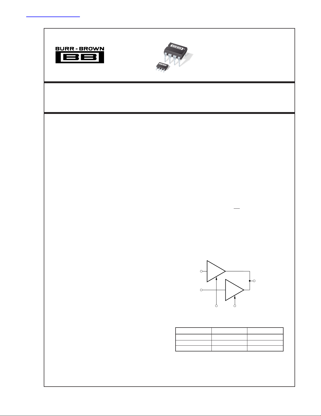
Wide-Bandwidth
2 x 1 VIDEO MULTIPLEXER
FEATURES
● BANDWIDTH: 210MHz (1.4Vp-p)
● LOW INTERCHANNEL CROSSTALK:
–79dB (30MHz, SO); –77dB (30MHz, DIP)
● LOW SWITCHING TRANSIENTS:
+13mV/–4mV
● LOW DIFFERENTIAL GAIN/PHASE
ERRORS: 0.03%, 0.01
● LOW QUIESCENT CURRENT:
One Channel Selected:
No Channel Selected:
APPLICATIONS
● VIDEO ROUTING AND MULTIPLEXING
(CROSSPOINTS)
● RADAR SYSTEMS
● DATA ACQUISITION
● INFORMATION TERMINALS
● SATELLITE OR RADIO LINK IF ROUTING
°
±4.6mA
±120µA
MPC104
The MPC104 consists of two identical monolithic,
integrated, open-loop buffer amplifiers, which are
connected internally at the output. The bipolar complementary buffers form a unidirectional transmission
path and offer extremely high output-to-input isolation. The MPC104 multiplexer enables the user to
connect one of two input signals to the output. The
output of the multiplexer is in a high-impedance state
when no channel is selected. When one channel is
selected with a digital “1” at the corresponding SEL
input, the component acts as a buffer with high input
impedance and low output impedance.
The wide bandwidth of over 210MHz at 1.4Vp-p
signal level, high linearity and low distortion, and low
input voltage noise of 5nV/√Hz make this crosspoint
switch suitable for RF and video applications. All
performance is specified with ±5V supply voltage,
which reduces power consumption in comparison with
±15V designs. The multiplexer is available in a spacesaving 8-pin SO and DIP packages. Both are designed
and specified for operation over the industrial temperature range (–40°C to +85°C.)
DESCRIPTION
The MPC104 is a wide-bandwidth, 2-to-1 channel
video signal multiplexer, which can be used in a wide
variety of applications.
IN
IN
+1
1
V
OUT
2
+1
It was designed for wide-bandwidth systems, including high-definition television and broadcast equipment. Although it is primarily used to route video
signals, the harmonic and dynamic attributes of the
MPC104 also make it appropriate for other analog
signal routing applications such as radar, communications, computer graphics, and data acquisition systems.
International Airport Industrial Park • Mailing Address: PO Box 11400, Tucson, AZ 85734 • Street Address: 6730 S. Tucson Blvd., Tucson, AZ 85706 • Tel: (520) 746-1111 • Twx: 910-952-1111
Internet: http://www.burr-brown.com/ • FAXLine: (800) 548-6133 (US/Canada Only) • Cable: BBRCORP • Telex: 066-6491 • FAX: (520) 889-1510 • Immediate Product Info: (800) 548-6132
©
1994 Burr-Brown Corporation PDS-1230C Printed in U.S.A. July, 1994
TRUTH TABLE
SEL
1
0 0 HI-Z
1 0IN
0 1IN
SEL
SEL
1
SEL
2
2
V
OUT
1
2

SPECIFICATIONS–DC CHARACTERISTICS
At VCC = ±5VDC, RL = 10kΩ, RIN = 100Ω, R
PARAMETER CONDITIONS MIN TYP MAX UNITS
INPUT OFFSET VOLTAGE
Initial 14 ±30 mV
vs Temperature 60 µV/°C
vs Supply (Tracking) V
vs Supply (Non-tracking) V
vs Supply (Non-tracking) V
Initial Matching All Buffers 3 mV
INPUT BIAS CURRENT
Initial 5 ±10 µA
vs Temperature 20 nA/°C
vs Supply (Tracking) V
vs Supply (Non-tracking) V
vs Supply (Non-tracking) V
INPUT IMPEDANCE
Resistance Channel On 0.88 MΩ
Capacitance Channel On 1.0 pF
Capacitance Channel Off 1.0 pF
INPUT NOISE
Voltage Noise Density f
Signal-to-Noise Ratio S/N = 0.7/V
INPUT VOLTAGE RANGE Gain Error ≤ 10% ±3.6 V
TRANSFER CHARACTERISTICS
Voltage Gain R
RATED OUTPUT
Voltage V
Resistance One Channel Selected 12.5 Ω
Resistance No Channel Selected 900 MΩ
Capacitance No Channel Selected 1.2 pF
CHANNEL SELECTION INPUTS
Logic 1 Voltage +2 V
Logic 0 Voltage +0.8 V
Logic 1 Current V
Logic 0 Current V
SWITCHING CHARACTERISTICS V
SEL to Channel ON Time 90% Point of V
SEL to Channel OFF Time 10% Point of V
Switching Transient, Positive (Measured While Switching +13 mV
Switching Transient, Negative Between Two Grounded Channels) –4 mV
POWER SUPPLY
Rated Voltage ±5V
Derated Performance ±4.5 ±5.5 V
Quiescent Current One Channel Selected, Over Temperature ±4.6 ±5.3 mA
Rejection Ratio –80 dB
= 50Ω, and TA = +25°C, unless otherwise noted.
SOURCE
MPC104AP, AU
= ±4.5V to ±5.5V –40 –80 dB
CC
= +4.5V to +5.5V –50 dB
CC
= –4.5V to –5.5V –50 dB
CC
= ±4.5V to ±5.5V ±710 nA/V
CC
= +4.5V to +5.5V 0.26 µA/V
CC
= –4.5V to –5.5V 1.7 µA/V
CC
= 20kHz to 10MHz 5 nV/√Hz
OUT
L
R
= 10kΩ, VIN = ±2.8V 0.98 0.992 V/V
L
= –0.3V to +0.7V, f = 5MHz
I
• √5MHz 96 dB
N
= 1kΩ, VIN = ±2V 0.982 V/V
= ±3V ±2.8 ±2.97 V
IN
+0.6 V
CC
= 5.0V 75 100 125 µA
SEL
= 0.8V 0.002 5 µA
SEL
= 1Vp-p 0.13 µs
OUT
= 1Vp-p 0.17 µs
OUT
No Channel Selected, Over Temperature ±120 ±175 µA
The information provided herein is believed to be reliable; however, BURR-BROWN assumes no responsibility for inaccuracies or omissions. BURR-BROWN assumes
no responsibility for the use of this information, and all use of such information shall be entirely at the user’s own risk. Prices and specifications are subject to change
without notice. No patent rights or licenses to any of the circuits described herein are implied or granted to any third party. BURR-BROWN does not authorize or warrant
any BURR-BROWN product for use in life support devices and/or systems.
®
MPC104
2

SPECIFICATIONS– AC CHARACTERISTICS
At VCC = ±5VDC, RL = 10kΩ, RIN = 100Ω, R
PARAMETER CONDITIONS MIN TYP MAX UNITS
LARGE SIGNAL BANDWIDTH (–3dB) V
SMALL SIGNAL BANDWIDTH V
GROUP DELAY TIME 550 ps
DIFFERENTIAL GAIN f = 4.43MHz, V
DIFFERENTIAL PHASE f = 4.43MHz, V
GAIN FLATNESS PEAKING V
HARMONIC DISTORTION f = 30MHz, V
Second Harmonic –63 dBc
Third Harmonic –65 dBc
CROSSTALK V
MPC104AP Channel-to-Channel f = 5MHz, –90 dB
Off Isolation f = 5MHz, –93 dB
MPC104AU Channel-to-Channel f = 5MHz, –95 dB
Off Isolation f = 5MHz, –93 dB
RISE/FALL TIME V
SLEW RATE V
= 50Ω, and TA = +25°C, unless otherwise noted.
SOURCE
MPC104AP, AU
= 5.0Vp-p, C
OUT
V
= 2.8Vp-p, C
OUT
V
= 1.4Vp-p, C
OUT
= 0.2Vp-p, C
OUT
VDC = 0 to 0.7V 0.03 %
VDC = 0 to 0.7V 0.01 Degrees
= 0.2Vp-p, DC to 30MHz 0.05 dB
OUT
V
= 0.2Vp-p, DC to 100MHz 0.07 dB
OUT
= 1.4Vp-p
IN
= 1pF 55 MHz
OUT
= 1pF 101 MHz
OUT
= 1pF 210 MHz
OUT
= 1pF 590 MHz
OUT
= 0.3Vp-p
IN
= 0.3Vp-p
IN
= 1.4Vp-p
OUT
f = 30MHz, –77 dB
f = 30MHz, –81 dB
f = 30MHz, –79 dB
f = 30MHz –86 dB
= 1.4Vp-p, Step 10% to 90%
OUT
C
= 1pF, R
OUT
OUT
C
C
C
OUT
OUT
= 22Ω 2.3 ns
OUT
= 1.4Vp-p
= 1pF 500 V/µs
OUT
= 22pF 360 V/µs
= 47pF 260 V/µs
®
3
MPC104
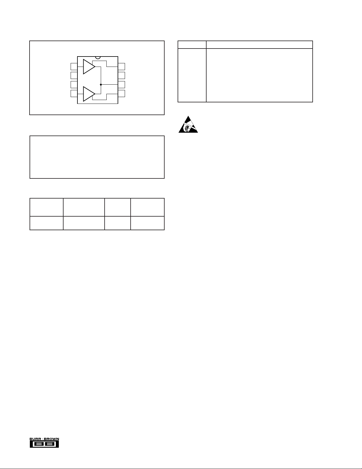
CONNECTION DIAGRAM
Top View DIP/SO-8
IN
GND
+V
IN
1
1
+1
2
CC
3
2
4
+1
SEL
1
8
–V
CC
7
V
OUT
6
SEL
2
5
PIN DESCRIPTION
PIN DESCRIPTION
IN
, IN
1
2
GND Analog Input Shielding Grounds,
, SEL
SEL
1
2
V
OUT
–V
CC
+V
CC
Analog Input Channels
Connect to System Ground
Channel Selection Inputs
Analog Output; tracks selected channel
Negative Supply Voltage; typical –5VDC
Positive Supply Voltage; typical +5VDC
ELECTROSTATIC
ABSOLUTE MAXIMUM RATINGS
Power Supply Voltage (±VCC) .........................................................±6VDC
Analog Input Voltage (IN
Operating Temperature..................................................... –40°C to +85°C
Storage Temperature...................................................... –40°C to +125°C
Output Current .................................................................................. ±6mA
Junction Temperature .................................................................... +175°C
Lead Temperature (soldering, 10s)................................................ +300°C
Digital Input Voltages (SEL
through IN2) ...................................±VCC, ±0.7V
1
through SEL2) .............. –0.5V to +VCC +0.7V
1
PACKAGE/ORDERING INFORMATION
PACKAGE
DRAWING TEMPERATURE
PRODUCT PACKAGE NUMBER
MPC104AP 8-Pin Plastic DIP 006 –40°C to +85°C
MPC104AU SO-8 Surface Mount 182 –40°C to +85°C
NOTE: (1) For detailed drawing and dimension table, please see end of data
sheet, or Appendix C of Burr-Brown IC Data Book.
(1)
RANGE
DISCHARGE SENSITIVITY
This integrated circuit can be damaged by ESD. Burr-Brown
recommends that all integrated circuits be handled with
appropriate precautions. Failure to observe proper handling
and installation procedures can cause damage.
ESD damage can range from subtle performance degradation to complete device failure. Precision integrated circuits
may be more susceptible to damage because very small
parametric changes could cause the device not to meet its
published specifications.
®
MPC104
4
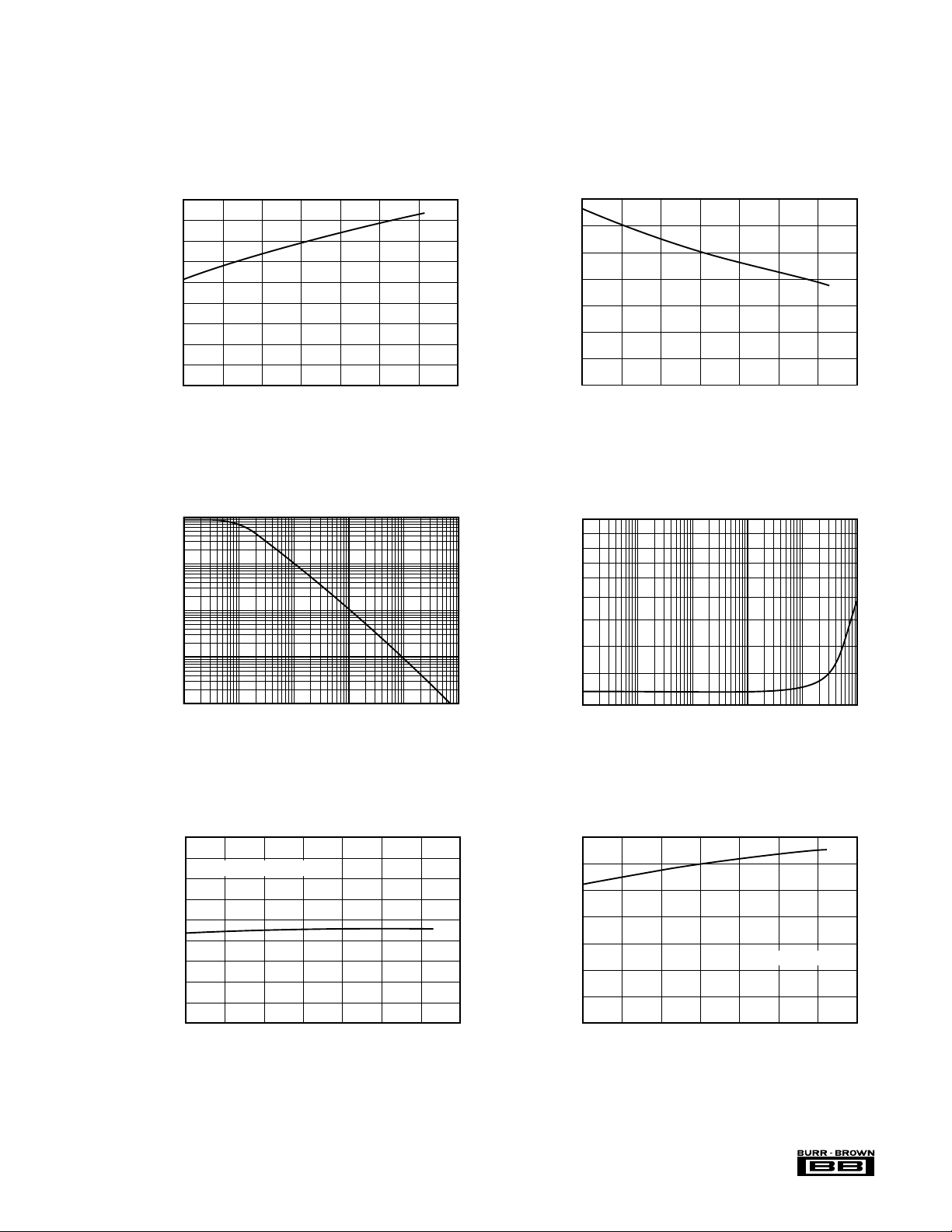
TYPICAL PERFORMANCE CURVES
–40 –20 0 20 60 80 100
Temperature (°C)
0
140
120
100
80
60
40
20
Supply Current (µA)
TOTAL POSITIVE QUIESCENT CURRENT
vs TEMPERATURE
40
No Channel Selected
At VCC = ±5VDC, RL = 10kΩ, RIN = 100Ω, R
= 50Ω, and TA = +25°C, unless otherwise noted.
SOURCE
18
16
14
12
10
Input Offset Voltage (mV)
1.0M
100k
10k
INPUT OFFSET VOLTAGE vs TEMPERATURE
8
6
4
2
0
–40 –20 0 20 60 80 100
Temperature (°C)
INPUT IMPEDANCE vs FREQUENCY
40
7
6
5
4
3
2
Input Bias Current (µA)
1
0
100
90
80
70
60
50
40
INPUT BIAS CURRENT vs TEMPERATURE
–40 –20 0 20 60 80 100
Temperature (°C)
OUTPUT IMPEDANCE vs FREQUENCY
40
Input Impedance (Ω)
1k
100
10k 100k 1M 10M 100M 1G
TOTAL POSITIVE QUIESCENT CURRENT
9
8
One Channel Selected
7
6
5
4
3
Supply Current (mA)
2
1
0
–40 –20 0 20 60 80 100
Frequency (Hz)
vs TEMPERATURE
40
Temperature (°C)
30
Output Impedance (Ω)
20
10
10k 100k 1M 10M 100M 1G
Frequency (Hz)
®
5
MPC104
 Loading...