

Page 1
MPC100
MPC100
查询MPC100供应商
®
Wide Bandwidth
4 x 1 VIDEO MULTIPLEXER
FEATURES
● BANDWIDTH: 250MHz (1.4Vp-p)
● LOW INTERCHANNEL CROSSTALK:
≤60dB (30MHz, DIP); ≤70dB (30MHz, SO)
● LOW SWITCHING TRANSIENTS:
+2.5/–1.2mV
● LOW DIFFERENTIAL GAIN/PHASE
ERRORS: 0.05%, 0.01
● LOW QUIESCENT CURRENT:
One Channel Selected:
No Channel Selected:
APPLICATIONS
● VIDEO ROUTING AND MULTIPLEXING
(CROSSPOINTS)
● RADAR SYSTEMS
● DATA ACQUISITION
● INFORMATION TERMINALS
● SATELLITE OR RADIO LINK IF ROUTING
°
±4.6mA
±230µA
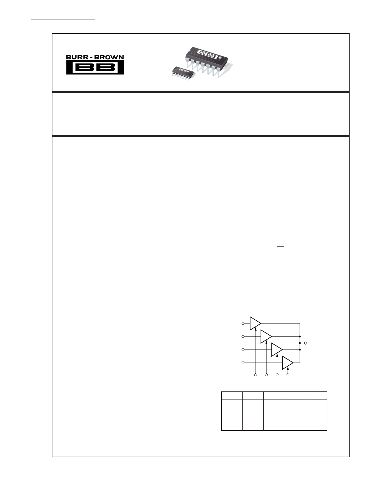
MPC100
The MPC100 consists of four identical monolithic integrated open-loop buffer amplifiers, which are connected internally at the output. The unidirectional transmission path consists of bipolar complementary buffers,
which offer extremely high output-to-input isolation.
The MPC100 multiplexer enables one of the four input
channels to connect to the output. The output of the
multiplexer is in a high-impedance state when no channel is selected. When one channel is selected with a
digital “1” at the corresponding SEL-input, the component acts as a buffer with high input impedance and low
output impedance.
The wide bandwidth of over 250MHz at 1.4Vp-p
signal level, high linearity and low distortion, and low
input voltage noise of 4nV/√Hz make this crosspoint
switch suitable for RF and video applications. All
performance is specified with ±5V supply voltage,
which reduces power consumption in comparison with
±15V designs. The multiplexer is available in spacesaving SO-14 and DIP packages. Both are designed
and specified for operation over the industrial temperature range (–40°C to +85°C.)
IN
1
DB1
DESCRIPTION
The MPC100 is a very wide bandwidth 4-to-1 channel
video signal multiplexer which can be used in a wide
IN
2
IN
3
DB2
DB3
V
OUT
variety of applications.
MPC100 is designed for wide-bandwidth systems,
4
DB4
IN
including high-definition television and broadcast
SEL
SEL
SEL
equipment. Although it is primarily used to route
video signals, the harmonic and dynamic attributes of
the MPC100 make it appropriate for other analog
TRUTH TABLE
SEL
signal routing applications such as radar, communications, computer graphics, and data acquisition systems.
International Airport Industrial Park • Mailing Address: PO Box 11400, Tucson, AZ 85734 • Street Address: 6730 S. Tucson Blvd., Tucson, AZ 85706 • Tel: (520) 746-1111 • Twx: 910-952-1111
Internet: http://www.burr-brown.com/ • FAXLine: (800) 548-6133 (US/Canada Only) • Cable: BBRCORP • Telex: 066-6491 • FAX: (520) 889-1510 • Immediate Product Info: (800) 548-6132
©
1991 Burr-Brown Corporation PDS-1133F Printed in U.S.A. March, 1995
SEL
SEL
1
0 0 0 0 HI-Z
1000IN
0100IN
0010IN
0001IN
2
1
SEL
2
4
3
SEL
3
V
4
OUT
1
2
3
4
Page 2

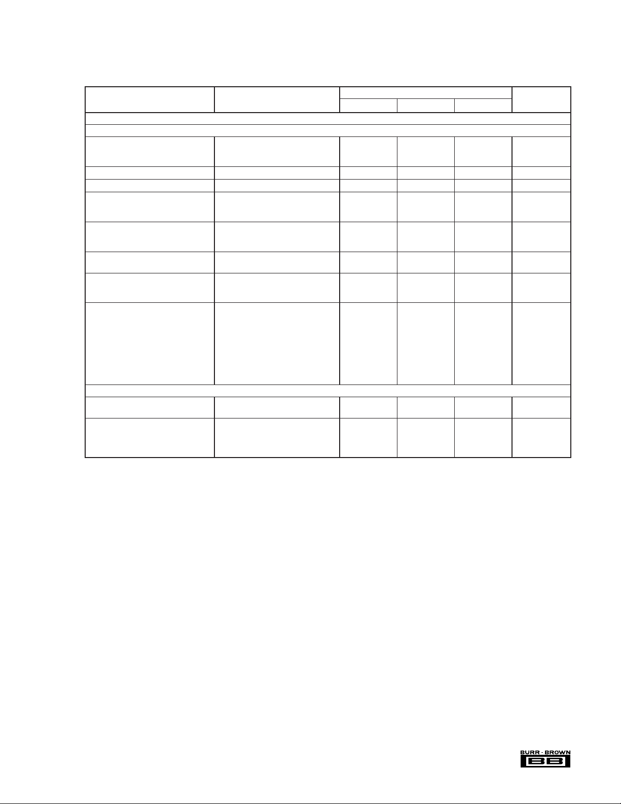
SPECIFICATIONS
At VCC = ±5V, RL = 10kΩ, R
PARAMETER CONDITIONS MIN TYP MAX UNITS
DC CHARACTERISTICS
INPUT OFFSET VOLTAGE R
Initial +10 ±30 mV
vs Temperature ±30 µV/°C
vs Supply (Tracking) V
vs Supply (Non-tracking) V
vs Supply (Non-tracking) V
Initial Matching Between the Four Channels ±3mV
INPUT BIAS CURRENT
Initial +4 ±10 µA
vs Temperature 20 nA/°C
vs Supply (Tracking) V
vs Supply (Non-tracking) V
vs Supply (Non-tracking) V
INPUT IMPEDANCE
Resistance Channel On 0.88 MΩ
Capacitance Channel On 1.0 pF
Capacitance Channel Off 1.0 pF
INPUT NOISE
Voltage Noise Density f
Signal-to-Noise Ratio S/N = 0.7/V
INPUT VOLTAGE RANGE Gain Error ≤ 10% ±4.2 V
TRANSFER CHARACTERISTICS Voltage Gain
CHANNEL SELECTION INPUTS
Logic 1 Voltage +2.0 V
Logic 0 Voltage 0 +0.8 V
Logic 1 Current V
Logic 0 Current V
SWITCHING CHARACTERISTICS V
SEL to Channel ON Time 90% Point of V
SEL to Channel OFF Time 10% Point of V
Switching Transient, Positive Measured While Switching +2.5 mV
Switching Transient, Negative Between Two Grounded Channels –1.2 mV
OUTPUT
Voltage V
Resistance One Channel Selected 11 Ω
Resistance No Channel Selected 900 MΩ
Capacitance No Channel Selected 1.5 pF
POWER SUPPLY
Rated Voltage ±5V
Derated Performance ±4.5 ±5.5 V
Quiescent Current One Channel Selected ±4.6 ±5mA
TEMPERATURE RANGE
Operating, AP, AU –40 +85 °C
Storage, AP, AU –40 +125 °C
Thermal Resistance,
θ
AP, AU 90 °C/W
= 50Ω, and TA = +25°C, unless otherwise noted.
SOURCE
= 0, R
IN
= ±4.5V to ±5.5V –40 –80 dB
CC
= +4.5V to +5.5V –50 dB
CC
= –4.5V to –5.5V –50 dB
CC
= ±4.5V to ±5.5V ±380 nA/V
CC
= +4.5V to +5.5V +1.0 µA/V
CC
= –4.5V to –5.5V –11.0 µA/V
CC
= 20kHz to 10MHz 4.0 nV/√Hz
B
= 1kΩ, VIN = ±2V 0.982 V/V
R
L
R
= 10kΩ, VIN = ±2.8V 0.98 0.992 V/V
L
SEL
SEL
= –0.3V to +0.7V, f = 5MHz
I
= ±3V, RL = 5kΩ±2.8 ±2.98 V
IN
No Channel Selected ±230 ±350 µA
JA
MPC100AP, AU
= 0
SOURCE
• √5MHz 98 dB
N
CC
= 5.0V 100 150 µA
= 0.8V 0.002 5 µA
= 1Vp-p 0.25 µs
O
= 1Vp-p 0.25 µs
O
V
The information provided herein is believed to be reliable; however, BURR-BROWN assumes no responsibility for inaccuracies or omissions. BURR-BROWN assumes
no responsibility for the use of this information, and all use of such information shall be entirely at the user’s own risk. Prices and specifications are subject to change
without notice. No patent rights or licenses to any of the circuits described herein are implied or granted to any third party. BURR-BROWN does not authorize or warrant
any BURR-BROWN product for use in life support devices and/or systems.
®
MPC100
2
Page 3
SPECIFICATIONS
At VCC = ±5V, RL = 10kΩ, R
PARAMETER CONDITIONS MIN TYP MAX UNITS
AC CHARACTERISTICS
FREQUENCY DOMAIN
LARGE SIGNAL BANDWIDTH (–3dB) V
SMALL SIGNAL BANDWIDTH V
GROUP DELAY TIME 450 ps
DIFFERENTIAL GAIN f = 4.43MHz, V
DIFFERENTIAL PHASE f = 4.43MHz, V
GAIN FLATNESS PEAKING V
HARMONIC DISTORTION f = 30MHz, V
Second Harmonic –53 dBc
Third Harmonic –67 dBc
CROSSTALK V
MPC100AP All Hostile f = 5MHz, –82 dB
Off Isolation f = 5MHz, –70 dB
MPC100AU All Hostile f = 5MHz, –78 dB
Off Isolation f = 5MHz, –75 dB
TIME DOMAIN
RISE TIME V
SLEW RATE V
= 50Ω, and TA = +25°C, unless otherwise noted.
SOURCE
= 5.0Vp-p, C
O
V
= 2.8Vp-p, C
O
V
= 1.4Vp-p, C
O
= 0.2Vp-p, C
O
IN
VDC = 0 to 0.7V 0.05 %
VDC = 0 to 1.4V 0.06 %
IN
VDC = 0 to 0.7V 0.01 Degrees
VDC = 0 to 1.4V 0.02 Degrees
= 0.2Vp-p, DC to 30MHz 0.04 dB
O
V
= 0.2Vp-p, DC to 100MHz 0.05 dB
O
= 1.4Vp-p, RL = 1kΩ
O
= 1.4Vp-p, Figures 4 and 8
I
f = 30MHz, –60 dB
f = 30MHz, –71 dB
f = 30MHz, –70 dB
f = 30MHz –76 dB
= 1.4Vp-p, Step 10% to 90%
O
C
= 1pF, R
OUT
OUT
= 2Vp-p
O
C
= 1pF 650 V/µs
OUT
C
= 22pF 460 V/µs
OUT
C
= 47pF 320 V/µs
OUT
MPC100AP, AU
= 1pF 70 MHz
OUT
= 1pF 140 MHz
OUT
= 1pF 250 MHz
OUT
= 1pF 450 MHz
OUT
= 0.3Vp-p
= 0.3Vp-p
= 22Ω 3.3 ns
®
3
MPC100
Page 4
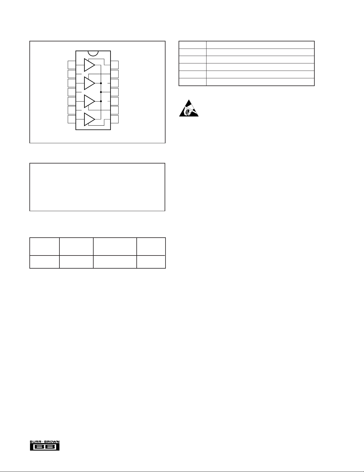
CONNECTION DIAGRAM
Top View DIP/SO-14
DB1
IN
GND
IN
GND
IN
GND
IN
1
1
2
DB2
3
2
4
DB3
5
3
6
DB4
7
4
MPC100
14
SEL
1
SEL
13
2
–V
12
CC
V
11
OUT
+V
10
CC
SEL
9
3
SEL
8
4
ABSOLUTE MAXIMUM RATINGS
Power Supply Voltage (±VCC) ..............................................................±6V
Analog Input Voltage (IN
Logic Input Voltage ................................................... –0.6V to +V
Operating Temperature..................................................... –40°C to +85°C
Storage Temperature...................................................... –40°C to +125°C
Output Current .................................................................................. ±6mA
Junction Temperature .................................................................... +175°C
Lead Temperature (soldering, 10s)................................................ +300°C
Digital Input Voltages (SEL
NOTE: (1) Inputs are internally diode-clamped to ±V
through IN4)
1
through SEL4)
1
(1)
................................±VCC, ±0.7V
CC
(1)
........... –0.5V to +VCC +0.7V
.
CC
+0.6V
FUNCTIONAL DESCRIPTION
IN1-IN
GND Analog input shielding grounds, connect to system ground
SEL
1
V
OUT
–V
CC
+V
CC
Four analog input channels
4
- SEL4Channel selection inputs
Analog output; tracks selected channel
Negative supply voltage; typical –5VDC
Positive supply voltage; typical +5VDC
ELECTROSTATIC
DISCHARGE SENSITIVITY
Electrostatic discharge can cause damage ranging from performance degradation to complete device failure. Burr-Brown
Corporation recommends that all integrated circuits be handled
and stored using appropriate ESD protection methods.
ESD damage can range from subtle performance degradation
to complete device failure. Precision integrated circuits may
be more susceptible to damage because very small parametric
changes could cause the device not to meet published specifications.
PACKAGE/ORDERING INFORMATION
PRODUCT RANGE PACKAGE NUMBER
TEMPERATURE DRAWING
MPC100AP –40°C to +85°C 14-Pin Plastic DIP 010
MPC100AU –40°C to +85°C SO-14 Surface Mount 235
NOTE: (1) For detailed drawing and dimension table, please see end of data
sheet, or Appendix C of Burr-Brown IC Data Book.
PACKAGE
(1)
®
MPC100
4
Page 5
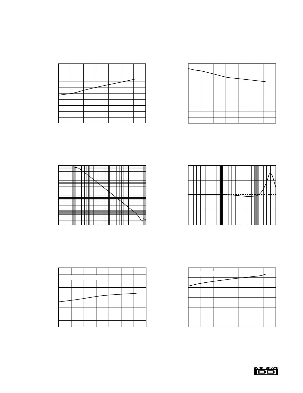
TYPICAL PERFORMANCE CURVES
–40 –20 0 20 60 80 100
Temperature (°C)
–5
5
4
3
2
1
0
–1
–2
–3
–4
Bias Current (µA)
INPUT BIAS CURRENT vs TEMPERATURE
40
At V
= ±5V, R
CC
LOAD
= 10kΩ, R
= 50Ω, and TA = +25°C, unless otherwise noted.
SOURCE
5
4
3
2
1
0
–1
Voltage (mV)
–2
–3
–4
–5
–40 –20 0 20 60 80 100
1.0M
100k
10k
OFFSET VOLTAGE vs TEMPERATURE
40
Temperature (°C)
INPUT IMPEDANCE vs FREQUENCY
100
OUTPUT IMPEDANCE vs FREQUENCY
30
10
Input Impedance (Ω)
1k
100
10k 100k 1M 10M 100M 1G
TOTAL QUIESCENT CURRENT vs TEMPERATURE
9
8
One Channel Selected
7
6
5
4
3
Supply Current (mA)
2
1
0
–40 –20 0 20 60 80 100
Frequency (Hz)
40
Temperature (°C)
3
Output Impedance (Ω)
1
10k 100k 1M 10M 100M 1G
Frequency (Hz)
TOTAL QUIESCENT CURRENT vs TEMPERATURE
300
No Channel Selected
250
200
150
100
Supply Current (µA)
50
0
–40 –20 0 20 60 80 100
Temperature (°C)
5
40
®
MPC100
Page 6

TYPICAL PERFORMANCE CURVES (CONT)
(µs)
At V
= ±5V, R
CC
LOAD
= 10kΩ, R
= 50Ω, and TA = +25°C, unless otherwise noted.
SOURCE
5
4
3
2
1
0
–1
–2
Output Voltage (V)
–3
–4
–5
–5–4–3–2–1012345
Output Voltage (V)
TRANSFER FUNCTION
Input Voltage (V)
SWITCHING ENVELOPE (Video Signal)
Time
+0.7V
0V
–0.3V
100
10
Voltage Noise (nV/ Hz)
0.1
12
10
Output Voltage (mV)
–2
–4
INPUT VOLTAGE NOISE SPECTRAL DENSITY
1
100 1k 100k 1M 10M 100M
SWITCHING TRANSIENTS (Channel To Channel)
SEL1
8
6
SEL2
4
2
0
0 20 40 60 80 100 120 140 160 180 200
10k
Frequency (Hz)
Without bandwidth
limiting lowpass filter.
Time (ns)
5V
5V
SWITCHING TRANSIENTS (Channel To Channel)
SEL1
SEL2
Output Voltage (mV)
–4
0 20 40 60 80 100 120 140 160 180 200
®
36MHz Low pass filter acc.
Eureka Rec. EU95-PG03
in the signal path.
Time (ns)
MPC100
5V
5V
SMALL SIGNAL PULSE RESPONSE
0 —
Output Voltage (40mV/Div)
= 1pF, t
OUT
(Generator) V
Time (ns)
= t
RISE
= 0.2Vp-p
I
FALL
= 2ns
C
6
Page 7

TYPICAL PERFORMANCE CURVES (CONT)
At V
= ±5VDC, R
CC
LOAD
= 10kΩ, R
= 50Ω, and TA = +25°C, unless otherwise noted.
SOURCE
SMALL SIGNAL PULSE RESPONSE
0 —
Output Voltage (40mV/Div)
C
= 47pF, t
OUT
(Generator) V
LARGE SIGNAL PULSE RESPONSE
0 —
Output Voltage (1V/Div)
= 47pF, t
C
OUT
(Generator) V
Time (ns)
RISE
I
Time (ns)
= t
RISE
= t
FALL
= 0.2Vp-p
= 5ns
FALL
= 5Vp-p
I
= 2ns
LARGE SIGNAL PULSE RESPONSE
0 —
Output Voltage (1V/Div)
Time (ns)
= 1pF, t
C
OUT
(Generator) V
RISE
= t
FALL
= 5Vp-p
I
= 5ns
GROUP DELAY TIME vs FREQUENCY
2.5
2
1.5
1
0.5
0
–0.5
Delay Time (ns)
V
–1
–1.5
–2
–2.5
1M 10M 100M 500M
150Ω
I
Group Delay Time
R
I
DUT
R
OUT
50Ω
V
OUT
300mV
Out
=
PO
Frequency (Hz)
20
15
10
5
0
–5
–10
Gain (dB)
–15
–20
–25
dB
BANDWIDTH vs C
R
C
OUT
WITH RECOMMENDED R
OUT
f
OUT
–3dB
OUT
1p 0Ω 500MHz
10p 22Ω 340MHz
250MHz
15Ω
22p
215MHz
12Ω
33p
130MHz
10Ω
47p
10pF
22pF
33pF
47pF
1M 10M 100M 1G
Frequency (Hz)
1pF
0.5
GAIN FLATNESS
0.4
0.3
0.2
0.1
0.2Vp-p
0
–0.1
Output (dB)
–0.2
R
= 150Ω, RO1 = 1kΩ
C
OUT
IN
= 22pF, R
OUT
= 15Ω
–0.3
–0.4
–0.5
300k
1M 10M 100M 1G
Frequency (Hz)
®
7
MPC100
Page 8

TYPICAL PERFORMANCE CURVES (CONT)
At V
= ±5V, R
CC
LOAD
= 10kΩ, R
= 50Ω, and TA = +25°C, unless otherwise noted.
SOURCE
20
15
10
5
0
–5
–10
Output (dBm)
–15
–20
C
–25
dB
20
15
10
5
0
–5
–10
Output (dBm)
–15
–20
C
–25
dB
300k
BANDWIDTH vs OUTPUT VOLTAGE
5Vp-p
2.8Vp-p
1.4Vp-p
0.6Vp-p
0.2Vp-p
OUT
= 1pF, R
OUT
= 0Ω
RIN = 150Ω
1M 10M 100M 1G300k
Frequency (Hz)
BANDWIDTH MATCHING (DB1...DB4)
2.8Vp-p
= 22pF, R
OUT
OUT
= 15Ω
1M 10M 100M 1G
Frequency (Hz)
BANDWIDTH vs R
LOAD
20
15
10
5
0
–5
–10
Output (dBm)
–15
–20
C
–25
= 22pF, R
OUT
RL = 500Ω = 1kΩ = 10kΩ
= 15Ω, VO = 2.8Vp-p
OUT
dB
1M
300k 10M 100M 1G
Frequency (Hz)
30MHz HARMONIC DISTORTION
10dB/Div
Harmonic Distortion (dB)
Frequency (Hz)
V
= 2.8Vp-p, RL = 1kΩ, C
OUT
OUT
= 1pF
®
MPC100
30MHz HARMONIC DISTORTION
10dB/Div
Harmonic Distortion (dB)
V
= 2.8Vp-p, RL = 10kΩ, C
OUT
Frequency (Hz)
8
OUT
= 1pF
Page 9

APPLICATIONS INFORMATION
The MPC100 operates from ±5V power supplies (±6V
maximum). Do not attempt to operate with larger power
supply voltages or permanent damage may occur. The buffer
outputs are not current-limited or protected. If the output is
shorted to ground, currents up to 18mA could flow. Momentary shorts to ground (a few seconds) should be avoided, but
are unlikely to cause permanent damage.
INPUT PROTECTION
All pins on the MPC100 are internally protected from ESD
by means of a pair of back-to-back reverse-biased diodes to
either power supply as shown in Figure 1. These diodes will
begin to conduct when the input voltage exceeds either
power supply by about 0.7V. This situation can occur with
loss of the amplifier’s power supplies while a signal source
is still present. The diodes can typically withstand a continuous current of 30mA without destruction. To insure long
term reliability, however, diode current should be externally
limited to 10mA or less whenever possible.
The internal protection diodes are designed to withstand
2.5kV (using Human Body Model) and will provide adequate ESD protection for most normal handling procedures. However, static damage can cause subtle changes in
amplifier input characteristics without necessarily destroying the device. In precision buffer amplifiers, this may cause
a noticeable degradation of offset voltage and drift. Therefore, static protection is strongly recommended when handling the MPC100.
Static damage has been well recognized for MOSFET devices, but any semiconductor device deserves protection
from this potentially damaging source. The MPC100 incorporates on-chip ESD protection diodes as shown in Figure 1.
This eliminates the need for the user to add external protection diodes, performance.
+V
–V
ESD Protection diodes
CC
internally connected to all pins.
Internal CircuitryExternal Pin
CC
FIGURE 1. Internal ESD Protection.
DISCUSSION
OF PERFORMANCE
The MPC100 video multiplexer allows the user to connect
any one of four analog input channels (IN
of the component and to switch between channels within
less than 0.5µs. It consists of four identical unity-gain buffer
amplifiers, which are connected together internally at the
output. The open loop buffers consisting of complementary
-IN4) to the output
1
emitter followers applies no feedback, so their low frequency gain is slightly less than unity and somewhat dependent on loading. Unlike devices using MOS bilateral switching elements, the bipolar complementary buffers form an
unidirectional transmission path and thus provide high output-to-input isolation. Switching stages compatible to TTL
level digital signals are provided for each buffer to select the
input channel. When no channel is selected, the output of the
device is high-impedance and allows the user to wire more
MPC100s together to form switch multi-channel matrices.
If one channel is selected with a digital “1” at the corresponding SEL-input, the MPC100 acts as a buffer amplifier
with high input impedance and low output impedance. The
truth table on the front page describes the relationship
between the digital inputs (SEL
inputs (IN
to IN4), and which signal is selected at the
1
to SEL4) and the analog
1
output.
The 2-4 address decoder and chip select logic is not
integrated. The selected design increases the flexibility of
address decoding in complex distribution fields, eases
BUS-controlled channel selection, simplifies channel selection monitoring for the user, and lowers transient peaks.
All of these characteristics make the multiplexer, in effect,
a quad switchable high-speed buffer. It requires DC coupling and termination resistors when directly driven from
a low impedance cable. High-current output amplifiers are
recommended when driving low-impedance transmission
lines or inputs.
An advanced complementary bipolar process, consisting of
pn-junction isolated high-frequency NPN and PNP transistors, provides wide bandwidth while maintaining low
crosstalk and harmonic distortion. The single chip bandwidth of over 250MHz at an output voltage of 1.4Vp-p
allows the design of large crosspoint or distribution fields
in HDTV-quality with an overall system bandwidth of
36MHz. The buffer amplifiers also offer low differential
gain (0.05%) and phase (0.01°) errors. These parameters
are essential for video applications and demonstrate how
well the signal path maintains a constant small-signal gain
and phase for the low-level color subcarrier at 4.43MHz
(PAL) or 3.58MHz (NSTC) as the brightness (luminance)
signal is ramped through its specified range. The bipolar
construction also ensures that the input impedance remains
high and constant between ON and OFF states. The ON/
OFF input capacitance ratio is near unity, and does not vary
with power supply voltage variations. The low output
capacitance of 1.5pF when no channel is selected is a very
important parameter for large distribution fields. Each parallel output capacitance is an additional load and reduces
the overall system bandwidth.
Bipolar video crosspoint switches are virtually glitch-free
when compared to signal switches using CMOS or DMOS
devices. The MPC100 operates with a fast make-beforebreak switching action to keep the output switching transients small and short. Switching from one channel to
another causes the signal to mix at the output for a short
time, but it interferes only minimally with the input signals.
®
9
MPC100
Page 10

The transient peaks remain less than +2.5mV and –1.2mV.
Subsequent equipment might interpret large negative output
glitches as synchronization pulses. To remove this problem,
the output must be clamped during the switching dead time.
With the MPC100, the generated output transients are extremely small and clamping is unnecessary. The switching
time between two channels is less than 0.5µs. This short
time period allows easy switching during the vertical blanking time. The signal envelope during the transition from one
channel to another rises and falls symmetrically and shows
less overshooting or DC settling transients.
Power consumption is a serious problem when designing
large crosspoint fields with high component density. Most of
the buffers are always in off-state. One important design
goal was to attain low off-state quiescent current when no
channel is selected. The low supply current of ±230µA in
off-state and ±4.6mA when one channel is selected, as well
as the reduced ±5V supply voltage, conserves power, simplifies the power supply design, and results in cooler, more
reliable operation.
CIRCUIT LAYOUT
The high-frequency performance of the MPC100 can be
greatly affected by the physical layout of the circuit. The
following tips are offered as suggestions, not as absolutes.
Oscillations, ringing, poor bandwidth and settling, higher
crosstalk, and peaking are all typical problems which plague
high-speed components when they are used incorrectly.
• Bypass power supplies very close to the device pins. Use
tantalum chip capacitors (approximately 2.2µF), a parallel
470pF ceramic chip capacitor may be added if desired.
Surface-mount types are recommended due to their low
lead inductance.
• PC board traces for signal and power lines should be wide
to reduce impedance or inductance.
• Make short and low inductance traces. The entire physical
circuit layout should be as small as possible.
• Use a low-impedance ground plane on the component side
to ensure that low-impedance ground is available throughout the layout. Grounded traces between the input traces
are essential to achieve high interchannel crosstalk rejection. Refer to the suggested layout shown in Figure 6.
• Do not extend the ground plane under high-impedance
nodes sensitive to stray capacitances, such as the buffer’s
input terminals.
• Sockets are not recommended because they add significant inductance and parasitic capacitance. If sockets are
required, use zero-profile solderless sockets.
• Use low-inductance and surface-mounted components to
achieve the best AC-performance.
• A resistor (100Ω to 200Ω) in series with the input of the
buffers may help to reduce peaking. Place the resistor as
close as possible to the pin.
• Plug-in prototype boards and wire-wrap boards will not
function well. A clean layout using RF techniques is
essential.
(13)
SEL
SEL
1
(14)
IN
1
DB1
(1)
GND
(2)
2
IN
2
(3)
DB2
GND
GND
(4)
IN
3
(5)
(6)
IN
4
(7)
SEL
(9)
DB3
SEL
(8)
DB4
+V
= +5V
CC
(10)
V
OUT
(11)
(12)
–V
= –5V
3
1
CC
FIGURE 2. Simplified Circuit Diagram.
®
MPC100
NOTE: DB = Diamond Buffer
10
Page 11

150Ω
10
0
–10
–20
–30
–40
–50
–60
–70
–80
Crosstalk (dB)
–90
MPC100AU
MPC100AP
Frequency (Hz)
10M 100M 300M1M
10
0
–10
–20
–30
–40
–50
–60
–70
–80
Frequency (Hz)
Crosstalk (dB)
10M 100M 300M
–90
MPC100AU
MPC100AP
1M
DB1
IN
50Ω
VI = 1.4Vp-p
1
GND
150Ω
V
I
50Ω
150Ω
IN
2
DB2
GND
IN
3
DB3
GND
DB4
IN
4
MPC100
SEL1
0
SEL2
0
SEL3
1
SEL4
0
15Ω 180Ω
22pF
BUF601
is connected to GND
IN
3
FIGURE 3. Channel Crosstalk—Grounded Input.
150Ω
DB1
IN
50Ω
VI = 1.4Vp-p
1
GND
150Ω
V
I
50Ω
200Ω
150Ω
IN
2
DB2
GND
IN
3
DB3
GND
DB4
IN
4
MPC100
SEL1
0
SEL2
0
SEL3
1
SEL4
0
15Ω 180Ω
22pF
is connected with 150Ω + 50Ω to GND
IN
3
BUF601
50Ω
V
O
Crosstalk = 20log
50Ω
V
O
Crosstalk = 20log
50Ω
V
O
V
I
50Ω
V
O
V
I
FIGURE 4. Channel Crosstalk—150Ω Input Resistor.
150Ω
DB1
IN
50Ω
VI = 1.4Vp-p
1
GND
150Ω
V
I
50Ω
150Ω
150Ω
GND
GND
IN
2
DB2
IN
3
DB3
DB4
IN
4
MPC100
180Ω
SEL1
SEL2
SEL3
SEL4
0
0
0
0
BUF601
V
Crosstalk = 20log
FIGURE 5. Off Isolation.
10
0
–10
–20
–30
50Ω
50Ω
O
V
O
V
I
–40
–50
Crosstalk (dB)
–60
–70
–80
–90
MPC100AU
MPC100AP
10M 100M 300M1M
Frequency (Hz)
®
11
MPC100
Page 12

2.2µ
470p
IN13
IN16
IN13
IN16
IN13
IN16
150Ω
75Ω
75Ω
75Ω
75Ω
75Ω
75Ω
75Ω
75Ω
75Ω
75Ω
75Ω
75Ω
1
2
150Ω
3
4
150Ω
5
6
150Ω
7
MPC100
150Ω
1
2
150Ω
3
4
150Ω
5
6
150Ω
7
MPC100
150Ω
1
2
150Ω
3
4
150Ω
5
6
150Ω
7
MPC100
–5V
14
13
12
22Ω
11
10
9
8
2.2µ
470p
2.2µ
470p
14
13
12
22Ω
11
10
9
8
2.2µ
470p
2.2µ
470p
14
13
12
22Ω
11
10
9
8
2.2µ
470p
2.2µ
470p
+5V
0.1µF
16
V
CC
15
14
13
12
11
10
15
14
13
12
11
10
1
Y
A
0
Y
A
1
Y
A
2
74HC
237
Y
CS1
3
Y
CS2
4
Y
5
9
Y
6
7
Y
LE
7
GND
+5V
0.1µF
16
V
CC
Y
A
0
Y
A
1
Y
A
2
74HC
237
Y
CS2
3
Y
CS1
4
Y
5
9
Y
6
7
Y
LE
7
GND
A
0
1
3
0
1
2
0
2
A
1
3
A
3
6
CS
5
+5V
4
1
2
3
5
6
4
FIGURE 6. Video Distribution Field.
®
MPC100
IN13
IN16
150Ω
75Ω
75Ω
75Ω
75Ω
1
2
150Ω
3
4
150Ω
5
6
150Ω
7
MPC100
14
13
12
22Ω
11
10
9
8
2.2µ
470p
+5V
+5V
2.2µ
10n
150Ω
3
7
+
75Ω
6
OPA623
2
–
220Ω
220Ω
Out
4
–5V
10n
2.2µ
12
Page 13

+5V
2.2µ
+5V
0.1µ
470p
BUF600
+5V
In
180Ω
75Ω
1
84
+1
5
–5V
150Ω
150Ω
75Ω
150Ω
75Ω
R-2R
Ladder
Network
150Ω
150Ω
75Ω
75Ω
150Ω
10
Y
15
14
1
DB1
2
3
DB2
4
5
DB3
13
14
Y
9
13
Y
12
8
Y
150Ω
11
6
7
DB4
GND
LE CS2
0
1
74HC
237
2
3
3
+
OPA623
2
–
390Ω
390 Ω
584
1
A
0
2
A
1
3
A
2
5
CS1
+5V
7
Out
75Ω
6
4
–5V
MPC100
12
–5V
2.2µ
470p
CS
0
0
0
0
1
1
0
0
1
1
X
A
GAINA
0
02
11
0.5
0
0.25
1
0
X
SEL
4
3
2
1
00
0
1
0
1
00
0
0
0
0
0
0
1
0
0
0
1
0
FIGURE 7. Digital Gain Control.
In1
In2
In3
In4
50Ω
50Ω
50Ω
50Ω
150Ω
150Ω
150Ω
150Ω
+5V
0.1µ
GND
LE CS2
12 Bit
10MHz
ADS804
584
1
A
0
2
A
1
3
A
2
5
CS1
+5V
–5V
16
V
CC
Y
15
0
Y
14
1
Y
13
2
12
Y
3
A/D Converter
7
6
Signal
Input
4
+5V
2.2µ
470p
10
14
1
DB1
2
3
DB2
4
5
DB3
6
7
DB4
MPC100
12
2.2µ
13
9
8
150Ω
11
3
+
OPA620
2
–
220Ω
220Ω
FIGURE 8. High Speed Data Acquisition System.
–5V
470p
13
®
MPC100
Page 14

CH1 G
CH2 G
CH3 G
CH4 G
150Ω
150Ω
150Ω
150Ω
150Ω
150Ω
150Ω
150Ω
150Ω
150Ω
150Ω
150Ω
1
DB1
2
3
DB2
4
5
DB3
6
7
DB4
MPC100
9101314
1
DB1
2
3
DB2
4
5
DB3
6
7
DB4
MPC100
9 10 13 14
9101314
1
DB1
2
3
DB2
4
5
DB3
6
7
DB4
MPC100
–5V
2.2µ
470p
12
2.2µ
470p
2.2µ
470p
2.2µ
470p
2.2µ
470p
2.2µ
470p
150Ω
150Ω
150
15
14
13
12
Ω
11
10
+5V
–5V
12
11
10
+5V
–5V
12
11
10
+5V
Y
Y
Y
Y
3
2
390Ω
3
2
390Ω
0
1
2
3
3
2
390Ω
+
OPA623
–
390Ω
+
OPA623
–
390Ω
CS1
74HC
237
CS2 GND
+
OPA623
–
390Ω
+5V
2.2µ
10n
7
6
4
–5V
+5V
2.2µ
10n
7
6
4
–5V
5
V
CC
LE
58
+5V
2.2µ
10n
7
6
4
–5V
75Ω
R
2.2µ
10n
75Ω
G
2.2µ
10n
+5V
16
CS
1
A
0
A
0
2
A
1
A
1
3
A
9
4
75Ω
B
2.2µ
10n
R
B
75
Ω
R
B
75Ω
R
B
75Ω
R
B
75Ω
FIGURE 9. Distribution Field for High Resolution Graphic Cards, Cameras.
®
MPC100
14
Page 15

50Ω
V
In
RIN =
50Ω
50Ω
Pulse
Generator
FIGURE 10. Test Circuit Pulse Response.
Out
R
R
I
150Ω
I
DB1
DUT
to DB4
R
OUT
O1
R
O1
+1
C
OUT
BUF601
R
B
51Ω
V
O
B
OUT
50Ω
400MHz
Scope
RIN =
50Ω
MPC100
V
75Ω
Generator
IN
DUT
RIN =
75Ω
75Ω 10kΩ
DB1 to DB4
4.43MHz
VDC
FIGURE 11. Test Circuit Differential Gain and Phase.
R
I
Generator
RIN =
50Ω
50Ω
In
50Ω
150Ω
V
I
DB1
DUT
to DB4
150Ω150Ω
4
+
3
–
75Ω
8
75Ω
390Ω
Video
Analyzer
RIN =
75Ω
390Ω
Out
R
OPA623
O1
R
OUT
R
O1
+1
C
OUT
BUF601
R
B
51Ω
V
O
B
OUT
50Ω
Spectrum
Analyzer
RIN =
50Ω
FIGURE 12. Test Circuit Frequency Response.
7
HC4094
MPC100
SEL Inputs
1143135127
SER
Out
11
2
3
31 15
SER In
Clock
STR
OE
MPC100
SEL Inputs
1435567
2
D
Parallel Out
31 15
FIGURE 13. Serial Bus-Controlled Distribution Field.
MPC100
SEL Inputs
MPC100
SEL Inputs
143556771143135127
Parallel Out
HC4094
SER
Out
15
MPC100
SEL Inputs
MPC100
SEL Inputs
143556771143135127
11
• • •
2
Parallel Out
HC4094
SER
Out
11
33
31 15
®
MPC100
 Loading...