

Burr Brown IVC102U, IVC102P, IVC102U-2K5 Datasheet
1
®
IVC102
I
IN
V
B
1
2
3
4
5
6
11 12 13
Digital
Ground
Analog
Ground
Logic Low closes switches
9
10
14
V
O
V+
V–
S
1
S
2
Ionization
Chamber
Photodiode
60pF
30pF
10pF
S
1
C
1
C
2
C
3
S
2
International Airport Industrial Park • Mailing Address: PO Box 11400 • Tucson, AZ 85734 • Street Address: 6730 S. Tucson Blvd. • Tucson, AZ 85706
Tel: (520) 746-1111 • Twx: 910-952-1111 • Cable: BBRCORP • Telex: 066-6491 • FAX: (520) 889-1510 • Immediate Product Info: (800) 548-6132
®
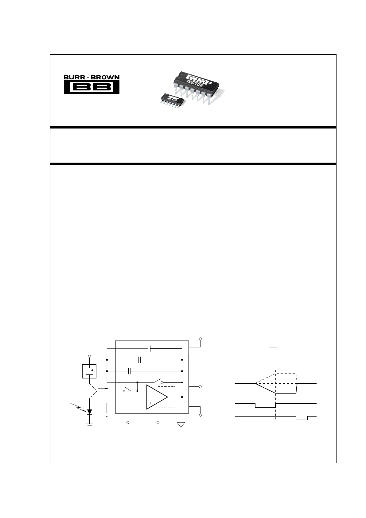
PRECISION SWITCHED INTEGRATOR
TRANSIMPEDANCE AMPLIFIER
APPLICA TIONS
● PRECISION LOW CURRENT MEASUREMENT
● PHOTODIODE MEASUREMENTS
● IONIZATION CHAMBER MEASUREMENTS
● CURRENT/CHARGE-OUTPUT SENSORS
● LEAKAGE CURRENT MEASUREMENT
IVC102
FEATURES
● ON-CHIP INTEGRATING CAPACITORS
● GAIN PROGRAMMED BY TIMING
● LOW INPUT BIAS CURRENT: 750fA max
● LOW NOISE
● LOW SWITCH CHARGE INJECTION
● FAST PULSE INTEGRATION
● LOW NONLINEARITY: 0.005% typ
● 14-PIN DIP, SO-14 SURFACE MOUNT
DESCRIPTION
The IVC102 is a precision integrating amplifier with
FET op amp, integrating capacitors, and low leakage
FET switches. It integrates low-level input current for
a user-determined period, storing the resulting voltage
on the integrating capacitor. The output voltage can be
held for accurate measurement. The IVC102 provides
a precision, lower noise alternative to conventional
transimpedance op amp circuits that require a very
high value feedback resistor.
The IVC102 is ideal for amplifying low-level sensor
currents from photodiodes and ionization chambers.
The input signal current can be positive or negative.
TTL/CMOS-compatible timing inputs control the integration period, hold and reset functions to set the
effective transimpedance gain and to reset (discharge)
the integrator capacitor.
Package options include 14-Pin plastic DIP and SO-14
surface-mount packages. Both are specified for the
–40°C to 85°C industrial temperature range.
© 1996 Burr-Brown Corporation PDS-1329A Printed in U.S.A. June, 1996
0V
Hold Integrate Hold Reset
Positive or Negative
Signal Integration
S
1
S
2
IIN(t)
V
O
=
–1
∫
dt
C
INT

2
®
IVC102
The information provided herein is believed to be reliable; however, BURR-BROWN assumes no responsibility for inaccuracies or omissions. BURR-BROWN assumes
no responsibility for the use of this information, and all use of such information shall be entirely at the user’s own risk. Prices and specifications are subject to change
without notice. No patent rights or licenses to any of the circuits described herein are implied or granted to any third party. BURR-BROWN does not authorize or warrant
any BURR-BROWN product for use in life support devices and/or systems.
NOTES: (1) Standard test timing: 1ms integration, 200µs hold, 100µs reset. (2) Hold mode output voltage after 1ms integration of zero input current. Includes op
amp offset voltage, integration of input error current and switch charge injection effects.
SPECIFICATIONS
At TA = +25°C, VS = ±15V, RL = 2kΩ, C
INT
= C1 + C2 + C3, 1ms integration period
(1)
, unless otherwise specified.
IVC102P, U
PARAMETER CONDITIONS MIN TYP MAX UNITS
TRANSFER FUNCTION V
O
= –(IIN)(T
INT
)/C
INT
Gain Error C
INT
= C1 + C2 + C
3
±5 +25/–17 %
vs Temperature ±25 ppm/°C
Nonlinearity V
O
= ±10V ±0.005 %
Input Current Range ±100 µA
Offset Voltage
(2)
IIN = 0, CIN = 50pF –5 ±20 mV
vs Temperature ±30 µV/°C
vs Power Supply V
S
= +4.75/–10 to +18/–18V 150 750 µV/V
Droop Rate, Hold Mode –1 nV/µs
OP AMP
Input Bias Current S
1
, S2 Open –100 ±750 fA
vs Temperature See Typical Curve
Offset Voltage (Op Amp V
OS
) ±0.5 ±5mV
vs Temperature ±5 µV/°C
vs Power Supply V
S
= +4.75/–10 to +18/–18V 10 100 µV/V
Noise Voltage f = 1kHz 10 nV/√Hz
INTEGRATION CAPACITORS
C
1
+ C2 + C
3
80 100 120 pF
vs Temperature ±25 ppm/°C
C
1
10 pF
C
2
30 pF
C
3
60 pF
OUTPUT
Voltage Range, Positive R
L
= 2kΩ (V+)–3 (V+)–1.3 V
Negative R
L
= 2kΩ (V–)+3 (V–)+2.6 V
Short-Circuit Current ±20 mA
Capacitive Load Drive 500 pF
Noise Voltage See Typical Curve
DYNAMIC CHARACTERISTIC
Op Amp Gain-Bandwidth 2 MHz
Op Amp Slew Rate 3V/µs
Reset
Slew Rate 3V/µs
Settling Time, 0.01% 10V Step 6 µs
DIGITAL INPUTS (TTL/CMOS Compatible)
V
IH
(referred to digital ground) (Logic High) 2 5.5 V
V
IL
(referred to digital ground) (Logic Low) –0.5 0.8 V
I
IH
VIH = 5V 2 µA
I
IL
VIL = 0V 0 µA
Switching Time 100 ns
POWER SUPPLY
Voltage Range: Positive +4.75 +15 +18 V
Negative –10 –15 –18 V
Current: Positive 4.1 5.5 mA
Negative –1.6 –2.2 mA
Analog Ground –0.2 mA
Digital Ground –2.3 mA
TEMPERATURE RANGE
Operating Range –40 85 °C
Storage –55 125 °C
Thermal Resistance,
θ
JA
DIP 100 °C/W
SO-14 150 °C/W
3
®
IVC102
ELECTROSTATIC
DISCHARGE SENSITIVITY
This integrated circuit can be damaged by ESD. Burr-Brown
recommends that all integrated circuits be handled with
appropriate precautions. Failure to observe proper handling
and installation procedures can cause damage.
ESD damage can range from subtle performance degradation to complete device failure. Precision integrated circuits
may be more susceptible to damage because very small
parametric changes could cause the device not to meet its
published specifications.
ABSOLUTE MAXIMUM RATINGS
Supply Voltage, V+ to V– .................................................................... 36V
Logic Input Voltage ...................................................................... V– to V+
Output Short Circuit to Ground ............................................... Continuous
Operating Temperature ................................................. –40°C to +125°C
Storage Temperature..................................................... –55°C to +125°C
Lead Temperature (soldering, 10s) ................................................. 300°C
PIN CONNECTIONS
Top View 14-Pin DIP/
SO-14 Surface Mount
PACKAGE INFORMATION
PACKAGE DRAWING
PRODUCT PACKAGE NUMBER
(1)
IVC102P 14-Pin DIP 010
IVC102U SO-14 Surface Mount 235
NOTE: (1) For detailed drawing and dimension table, please see end of data
sheet, or Appendix D of Burr-Brown IC Data Book.
V+
Digital Ground
S
2
S
1
V
O
V–
NC
Analog Ground
I
IN
–In
C
1
C
2
C
3
NC
NC = No Internal Connection
Connect to Analog Ground for Lowest Noise
14
13
12
11
10
9
8
1
2
3
4
5
6
7
 Loading...