

Burr Brown ISO422P Datasheet
®
ISO422
ISO422
ISO422
DIFFERENTIAL BUS TRANSCEIVER
FEATURES
● FULL-/HALF-DUPLEX OPERATION
● 1500Vrms ISOLATION (cont)
● 2500Vrms ISOLATION (1 min)
● 2.5Mbps PERFORMANCE
● LOOP-TEST FACILITY
APPLICATIONS
● BUS TRANSMISSION SYSTEMS
● GROUND LOOP ISOLATION
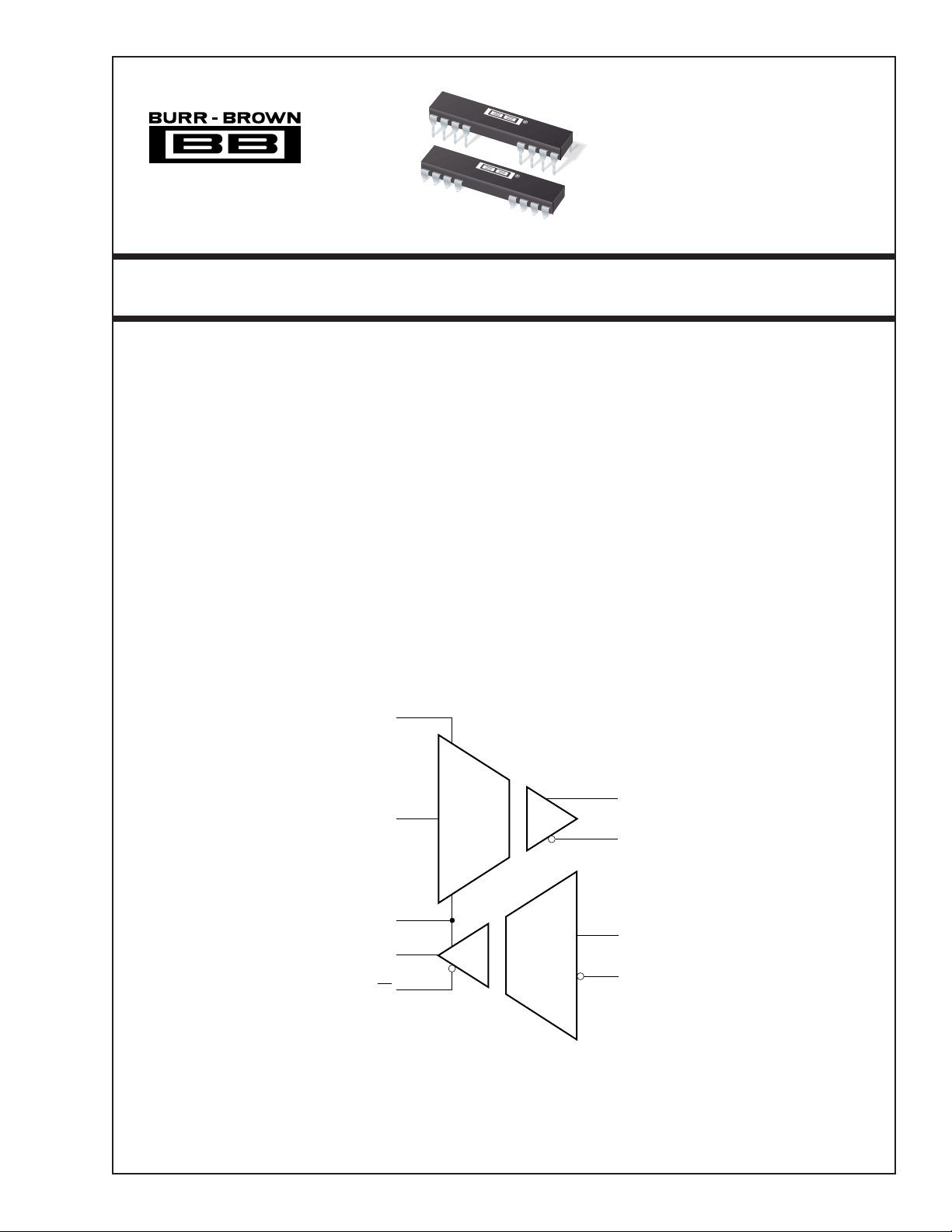
DE
D
DESCRIPTION
ISO422 provides 1500Vrms isolation for industrial
bus transmission systems. ISO422 may be configured
in full or half duplex modes providing the user with
best flexibility for the application. Transmission rates
of 2.5Mbps can be obtained covering most requirements. A loop-back test facility is included. LBE
allows data on the D input to be routed to the R output
for test purposes.
ISO422 is available in 24-pin PDIP and 24-pin Gull
(1)
Wing
packages and is specified over the temperature
range –40°C to +85°C.
NOTE: (1) Gull Wing version available Q1’99.
Y
Z
LBE
R
RE
International Airport Industrial Park • Mailing Address: PO Box 11400, Tucson, AZ 85734 • Street Address: 6730 S. Tucson Blvd., Tucson, AZ 85706 • Tel: (520) 746-1111
Twx: 910-952-1111 • Internet: http://www.burr-brown.com/ • Cable: BBRCORP • Telex: 066-6491 • FAX: (520) 889-1510 • Immediate Product Info: (800) 548-6132
©
1998 Burr-Brown Corporation PDS-1503A Printed in U.S.A. December, 1998
A
B

SPECIFICATIONS
At TA = +25°C, and VS = +5V, unless otherwise noted.
ISO422P, P-U
(1)
PARAMETER CONDITIONS MIN TYP MAX UNITS
ISOLATION
Rated Continuous Isolation V
ISO
Partial Discharge Voltage 1s, 5 x 5pC/per cycle
50Hz, 60Hz 1500 V
(2)
2500 V
Barrier Impedance > 1014 || 10 Ω || pF
Leakage Current 240V, 60Hz 1 µA
2500V, 50Hz 10 µA
Creepage Distance 8.6 mm
Internal Isolation Distance 0.1 mm
Transient Recovery Time 5kV/µs Edge 1 µs
DRIVER DC CHARACTERISTICS
High Level Input Voltage V
Low Level Input Voltage V
Input Leakage Current I
Input Capacitance C
Output Voltage V
Differential Output Voltage V
IH
IL
L
IN
O
OD
D and DE Inputs
D and DE Inputs
D and DE Inputs
D and DE Inputs
VY or V
IOY or IOZ = 0 1.5 5 V
(3)
(3)
(3)
(3)
Z
2V
0.8 V
5nA
5pF
05V
RL = 100Ω 2 3.6 5 V
Change in Mag Diff Out Voltage ∆|V
Common-Mode Output Voltage V
Change in Mag CM Out Voltage ∆|VOC|R
Output Current I
|R
OD
OC
O
= 100Ω or 54Ω
L
RL = 100Ω or 54Ω 3V
= 100Ω or 54Ω
L
VO = V
CC2
, Output Disabled ±10 ±1000 nA
RL = 54Ω 1.5 2.8 5 V
(4)
(4)
±40 ±200 mV
±40 ±200 mV
VO = 0V, Output Disabled ±10 ±1000 nA
Short-Circuit Output Current VO = V
, Continuous 100 mA
CC2
V
= 0V, Continuous –110 mA
O
DRIVER SWITCHING CHARACTERISTICS (Figure 6)
Differential Output Delay Time t
Skew |t
DDH
- t
|R
DDL
Differential Output Transition Time t
Output Enable Time to HIGH t
Output Enable Time to LOW t
Output Disable Time from HIGH t
Output Disable Time from LOW t
DD
DT
DZH
DZL
DHZ
DLZ
RL = 54Ω 120 150 ns
= 54Ω 25 50 ns
L
RL = 54Ω 100 ns
RL = 100Ω 120 150 ns
RL = 100Ω 120 150 ns
RL = 100Ω 120 150 ns
RL = 100Ω 120 150 ns
RECEIVER DC CHARACTERISTICS
High Level Output Voltage V
Low Level Output Voltage V
Output Short-Circuit Current I
Output HI-Z Leakage I
Enable Input HIGH Threshold V
Enable Input LOW Threshold V
Input Leakage Current I
Input Capacitance C
Differential Input HIGH Threshold V
Differential Input LOW Threshold V
OH
OL
OS
OZ
IH
IL
L
IN
TH
TL
IOH = 6mA V
– 1 V
CC
IOL = 6mA 0.4 V
1s max 30 mA
V
= 0V to V
OUT
RE Input
RE Input
RE Input
RE Input
CC1
(3)
(3)
(3)
(3)
2V
±10 ±1000 nA
0.8 V
5nA
5pF
VO = 2.8V 100 200 mV
VO = 0.4V –200 –100 mV
Input Hysteresis See Note 5 60 mV
Line Input Current I
Line Voltage V
Input Resistance R
Power On (GNDB < VBI < VSB) ±10 ±1000 nA
BI
Power Off (IBI ±10mA max) ±12 V
BI
IN
1MΩ
RECEIVER SWITCHING CHARACTERISTICS (Figure 7)
Propagation Delay L to H t
Propagation Delay H to L t
Skew |t
- t
| 40 ns
RLH
RHL
Output Rise Time t
Output Fall Time t
Output Enable Time to HIGH t
Output Enable Time to LOW t
Output Disable Time from HIGH t
Output Disable Time from LOW t
VID = –1.5V to 1.5V, CL = 10pF 120 150 ns
RLH
VID = 1.5V to –1.5V, CL = 10pF 120 150 ns
RHL
R
F
RZH
RZL
RHZ
RLZ
CL = 10pF 10 ns
CL = 10pF 10 ns
CL = 10pF 15 25 ns
CL = 10pF 15 25 ns
CL = 10pF 15 25 ns
CL = 10pF 15 25 ns
®
ISO422
2
SPECIFICATIONS (CONT)
At TA = +25°C, and VS = +5V, unless otherwise noted.
ISO422P, P-U
PARAMETER CONDITIONS MIN TYP MAX UNITS
POWER
Supply Voltage—Data Side V
Supply Current—Data Side I
Supply Current—Data Side I
Supply Voltage—Bus Side V
Supply Voltage—Bus Side I
BUS LIMITS
Input Current ±10 mA
Maximum Differential Input ±5V
Maximum Data Rate 2.5 Mbps
TEMPERATURE RANGE
Operating –40 +85 °C
Storage –40 +125 °C
Thermal Resistance
NOTES: (1) Gull Wing version available Q1’99. (2) All devices receive a 1s test. Failure criterion is > 5 pulses of > 5pC per cycle. (3) Logic inputs are HCT-type
and thresholds are a function of power supply voltage with approximately 100mV hysteresis. (4) Change in magnitude when the input is changed from HIGH to
LOW. (5) The difference between the differential low to high and high to low transition points.
PIN CONFIGURATION
Top View DIP
1
DE
2
D
3
NC
4
V
SA
SA
SA
SA
SB
SB
θ
JA
Output Unloaded, dc 10 13 mA
Output Unloaded, max Rate 20 mA
Output Unloaded, dc 12 20 mA
Output Unloaded, max Rate 20 mA
ABSOLUTE MAXIMUM RATINGS
Supply Voltage: VSA............................................................. –0.5V to +6V
Continuous Isolation Voltage .....................................................1500Vrms
Storage Temperature...................................................... –40°C to +125°C
Lead Temperature (soldering, 10s) ............................................... +300°C
24
RE
23
R
22
LBE
21
GND
A
PACKAGE INFORMATION
PRODUCT PACKAGE NUMBER
ISO422P 24-Pin Plastic DIP 243-4
ISO422P-U 24-Pin Gull Wing Surface Mount 243-5
NOTE: (1) For detailed drawing and dimension table, please see end of data
sheet, or Appendix C of Burr-Brown IC Data Book.
4.5 5.5 V
4.5 5.5 V
............................................................. –0.5V to +6V
V
SB
(1)
75 °C/W
PACKAGE DRAWING
(1)
GND
GND
9
B
10
B
11
Y
12
Z
16
V
SB
15
V
SB
14
A
13
B
Electrostatic discharge can cause damage ranging from per-
ELECTROSTATIC
DISCHARGE SENSITIVITY
formance degradation to complete device failure. BurrBrown Corporation recommends that all integrated circuits
be handled and stored using appropriate ESD protection
methods.
ESD damage can range from subtle performance degradation to complete device failure. Precision integrated circuits
may be more susceptible to damage because very small
parametric changes could cause the device not to meet
published specifications.
The information provided herein is believed to be reliable; however, BURR-BROWN assumes no responsibility for inaccuracies or omissions. BURR-BROWN
assumes no responsibility for the use of this information, and all use of such information shall be entirely at the user’s own risk. Prices and specifications are subject
to change without notice. No patent rights or licenses to any of the circuits described herein are implied or granted to any third party. BURR-BROWN does not
authorize or warrant any BURR-BROWN product for use in life support devices and/or systems.
3
ISO422
®
 Loading...