

Burr Brown ISO175P Datasheet
®
ISO175
Precision, Isolated
INSTRUMENT ATION AMPLIFIER
ISO175
FEATURES
● RATED
1500Vrms Continuous
2500Vrms for One Minute
100% TESTED FOR PARTIAL DISCHARGE
● HIGH IMR: 115dB at 50Hz
● LOW NONLINEARITY:
±0.01%
● LOW INPUT BIAS CURRENT: 10nA max
● LOW INPUT OFFSET VOLTAGE: 101mV max
● INPUTS PROTECTED TO
● BIPOLAR OPERATION: V
±40V
= ±10V
O
● SYNCHRONIZATION CAPABILITY
● 24-PIN PLASTIC DIP: 0.3" Wide
APPLICATIONS
● INDUSTRIAL PROCESS CONTROL
Transducer Isolator, Thermocouple
Isolator, RTD Isolator, Pressure Bridge
Isolator, Flow Meter Isolator
● POWER MONITORING
● MEDICAL INSTRUMENTATION
● ANALYTICAL MEASUREMENTS
● BIOMEDICAL MEASUREMENTS
● DATA ACQUISITION
● TEST EQUIPMENT
● POWER MONITORING
● GROUND LOOP ELIMINATION
V
1
IN–
R
22
G
2
R
G
24
V
IN+
DESCRIPTION
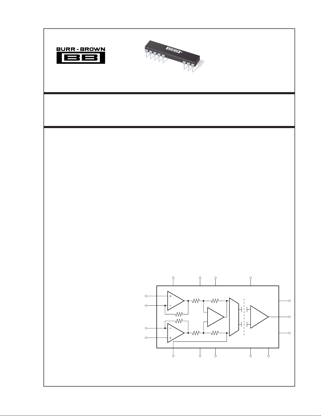
ISO175 is a precision isolated instrumentation amplifier incorporating a novel duty cycle modulationdemodulation technique and excellent accuracy. A
single external resistor sets the gain. Internal input
protection can withstand up to ±40V without damage.
The signal is transmitted digitally across a differential
capacitive barrier. With digital modulation the barrier
characteristics do not affect signal integrity. This results in excellent reliability and good high frequency
transient immunity across the barrier. Both the amplifier and barrier capacitors are housed in a plastic DIP.
ISO175 is easy to use. A power supply range of ±4.5V
to ±18V makes this amplifier ideal for a wide range of
applications.
5214 15
Shield 1 Ext Osc +V
S1
+V
S2
Shield 2
V
OUT
Com2
14
11
10
Com1
23 20 3 13 12
International Airport Industrial Park • Mailing Address: PO Box 11400, Tucson, AZ 85734 • Street Address: 6730 S. Tucson Blvd., Tucson, AZ 85706 • Tel: (520) 746-1111 • Twx: 910-952-1111
Internet: http://www.burr-brown.com/ • FAXLine: (800) 548-6133 (US/Canada Only) • Cable: BBRCORP • Telex: 066-6491 • FAX: (520) 889-1510 • Immediate Product Info: (800) 548-6132
©
1996 Burr-Brown Corporation PDS-1293A Printed in U.S.A. May, 1996
GND1 –V
S1
–V
GND2
S2
SPECIFICATIONS
At TA = +25°C, VS1 = VS2 = ±15V, and RL = 2kΩ unless otherwise noted.
ISO175P
PARAMETER CONDITIONS MIN TYP MAX UNITS
ISOLATION
Voltage Rated Continuous:
AC T
DC T
100% Test (AC, 50Hz) 1s; Partial Discharge ≤ 5pC 2500 Vrms
Isolation-Mode Rejection
AC 50Hz 1500Vrms 115 dB
DC 160 dB
Barrier Impedance 10
Leakage Current VISO = 240Vrms, 50Hz 0.8 1 µArms
GAIN
Gain Error G = 1 ±0.35 %
Gain vs Temperature G = 1 ±11 ppm/°C
Nonlinearity G = 1 ±0.102 %
INPUT OFFSET VOLTAGE
Initial Offset G = 1, 100 mV
vs Temperature µV/°C
vs Supply G = 1 ±2 mV/V
INPUT
Voltage Range ±10 V
Bias Current ±10 nA
vs Temperature ±40 pA/°C
Offset Current ±10 nA
vs Temperature ±40 pA/°C
OUTPUT
Voltage Range ±10 V
Current Drive ±5mA
Capacitive Load Drive 0.1 µF
Ripple Voltage 10 mVp-p
FREQUENCY RESPONSE
Small Signal Bandwidth G = 1 60 kHz
Slew Rate V
POWER SUPPLIES
Rated Voltage 15 V
Voltage Range ±4.5 ±18 V
Quiescent Current
V
V
TEMPERATURE RANGE
Operating –40 85 °C
Storage –40 125 °C
NOTE: (1) All devices receive a 1s test. Failure criterion is ≥ 5 pulses of ≥ 5pc.
(1)
MIN
MIN
to T
to T
MAX
MAX
1500 Vrms
2121 VDC
14
|| 6 Ω || pF
50k
1+
R
G
V/V
G = 10 ±0.07 %
G = 100 ±0.95 %
G = 10 ±0.04 %
G = 100 ±0.104 %
101
± 1+
520
G
± 0.125 +
G
G = 10 60 kHz
G = 100 50 kHz
= ±10V, G = 10 0.9 V/µs
O
S1
S2
±7.4 mA
±7.5 mA
®
ISO175
2
V
S1–
V
S1+
Shield 1
Com 2
V
OUT
GND 2
R
G
EXT OSC
GND 1
V
S2+
Shield 2
V
S2–
R
G
Com 1
V
IN–
1
2
3
4
5
10
11
12
24
23
22
21
20
15
14
13
V
IN+
ABSOLUTE MAXIMUM RATINGS
Supply Voltage................................................................................... ±18V
Analog Input Voltage Range .............................................................. ±40V
External Oscillator Input..................................................................... ±25V
Com 1 to GND1 ................................................................................... ±1V
Com 2 to GND2 ................................................................................... ±1V
Continuous Isolation Voltage: ....................................................1500Vrms
IMV, dv/dt...................................................................................... 20kV/µs
Junction Temperature ...................................................................... 150°C
Storage Temperature...................................................... –40°C to +125°C
Lead Temperature (soldering, 10s)................................................ +300°C
Output Short Duration .......................................... Continuous to Common
ELECTROSTATIC
DISCHARGE SENSITIVITY
Any integrated circuit can be damaged by ESD. Burr-Brown
recommends that all integrated circuits be handled with
appropriate precautions. Failure to observe proper handling
and installation procedures can cause damage.
ESD damage can range from subtle performance degradation to complete device failure. Precision integrated circuits
may be more susceptible to damage because very small
parametric changes could cause the device not to meet
published specifications.
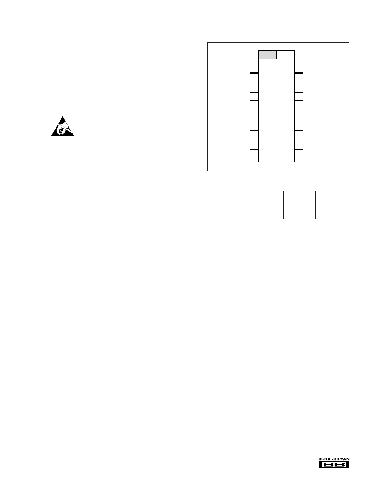
PIN CONFIGURATION
PACKAGE/ORDERING INFORMATION
PACKAGE
DRAWING
PRODUCT PACKAGE NUMBER
ISO175P 24-Pin Plastic DIP 243-2 60kHz
NOTE: (1) For detailed drawing and dimension table, please see end of data
sheet, or Appendix C of Burr-Brown IC Data Book.
(1)
BANDWIDTH
The information provided herein is believed to be reliable; however, BURR-BROWN assumes no responsibility for inaccuracies or omissions. BURR-BROWN assumes
no responsibility for the use of this information, and all use of such information shall be entirely at the user's own risk. Prices and specifications are subject to change
without notice. No patent rights or licenses to any of the circuits described herein are implied or granted to any third party. BURR-BROWN does not authorize or warrant
any BURR-BROWN product for use in life support devices and/or systems.
3
ISO175
®
 Loading...