

Page 1
®
40kΩ
10kΩ
10kΩ
40kΩ
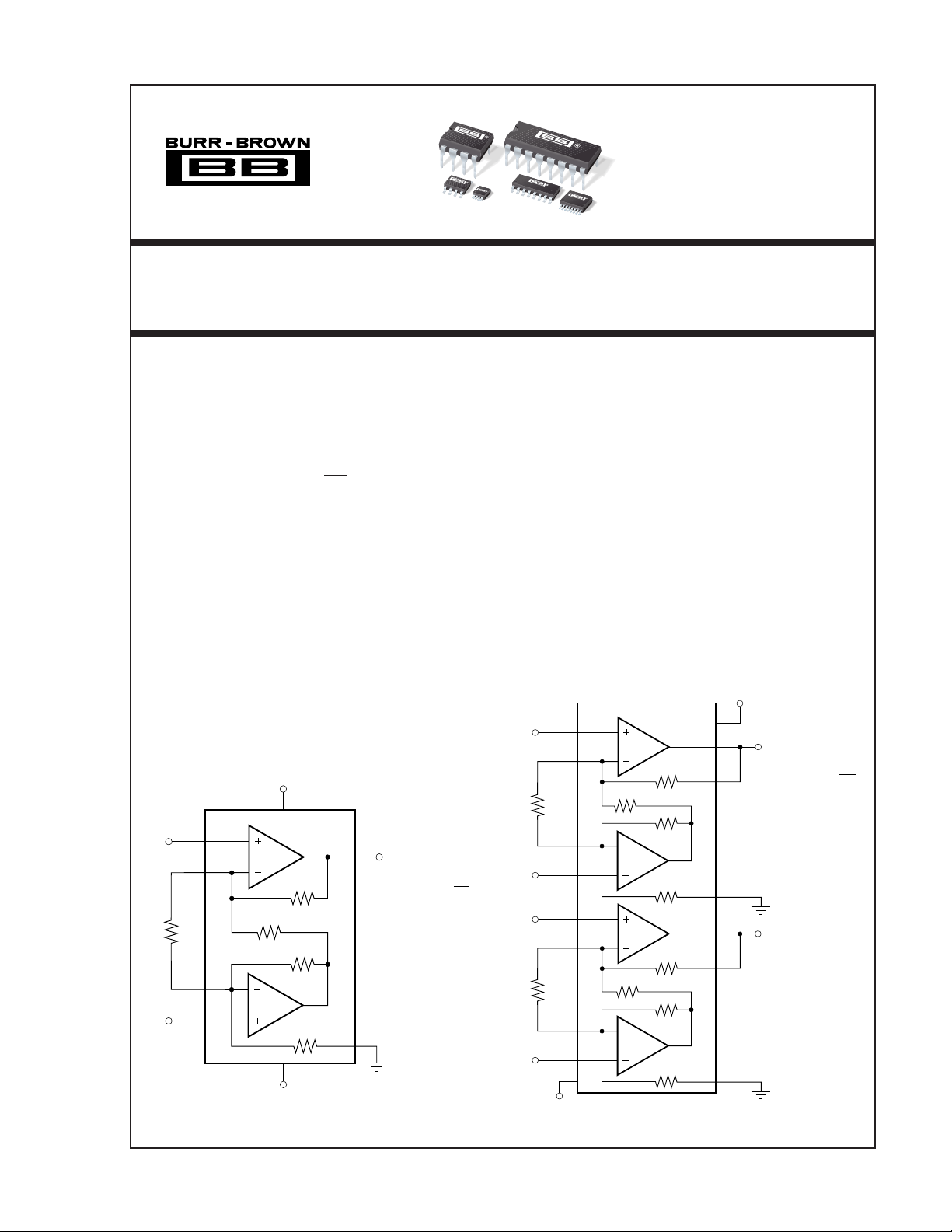
INA2126
5
7
8
1
3
4
2
9
6
R
G
V
IN
–
V
IN
+
V+
V–
V
O
= (V
IN
– VIN) G
–
+
80k
R
G
G = 5 +
V
O
= (VIN – VIN) G
–
+
80k
R
G
G = 5 +
40kΩ
10kΩ
10kΩ
40kΩ
12
16
14
13
15
11
10
R
G
V
IN
–
V
IN
+
INA126
INA2126
INA126
INA126
INA2126
INA2126
INA2126
Micro
POWER INSTRUMENTATION AMPLIFIER
Single and Dual Versions
FEATURES
● LOW QUIESCENT CURRENT: 175µA/chan.
● WIDE SUPPLY RANGE:
● LOW OFFSET VOLTAGE: 250
● LOW OFFSET DRIFT: 3
● LOW NOISE: 35nV/√Hz
● LOW INPUT BIAS CURRENT: 25nA max
● 8-PIN DIP, SO-8, MSOP-8 SURFACE- MOUNT
DUAL: 16-Pin DIP, SO-16, SSOP-16
APPLICATIONS
● INDUSTRIAL SENSOR AMPLIFIER:
Bridge, RTD, Thermocouple
● PHYSIOLOGICAL AMPLIFIER:
ECG, EEG, EMG
● MULTI-CHANNEL DATA ACQUISITION
● PORTABLE, BATTERY OPERATED SYSTEMS
±1.35V to ±18V
µV max
µV/°C max
DESCRIPTION
The INA126 and INA2126 are precision instrumentation
amplifiers for accurate, low noise differential signal acquisition. Their two-op-amp design provides excellent performance with very low quiescent current (175µA/chan.). This,
combined with wide operating voltage range of ±1.35V to
±18V, makes them ideal for portable instrumentation and data
acquisition systems.
Gain can be set from 5V/V to 10000V/V with a single
external resistor. Laser trimmed input circuitry provides
low offset voltage (250µV max), low offset voltage drift
(3µV/°C max) and excellent common-mode rejection.
Single version package options include 8-pin plastic DIP,
SO-8 surface mount, and fine-pitch MSOP-8 surface-mount.
Dual version is available in the space-saving SSOP-16 finepitch surface mount, SO-16, and 16-pin DIP. All are specified for the –40°C to +85°C industrial temperature range.
V+
+
V
IN
–
V
IN
International Airport Industrial Park • Mailing Address: PO Box 11400, Tucson, AZ 85734 • Street Address: 6730 S. Tucson Blvd., Tucson, AZ 85706 • Tel: (520) 746-1111 • Twx: 910-952-1111
Internet: http://www.burr-brown.com/ • FAXLine: (800) 548-6133 (US/Canada Only) • Cable: BBRCORP • Telex: 066-6491 • FAX: (520) 889-1510 • Immediate Product Info: (800) 548-6132
©1996 Burr-Brown Corporation PDS-1365C Printed in U.S.A. September, 1997
3
8
R
G
1
2
7
40kΩ
10kΩ
10kΩ
40kΩ
4
V–
INA126
6
5
= (VIN – VIN) G
V
O
G = 5 +
–+
80k
R
G
Page 2
SPECIFICATIONS
At TA = +25°C, VS = ±15V, RL = 25kΩ, unless otherwise noted.
INA126P, U, E INA126PA, UA, EA
INA2126P, U, E INA2126PA, UA, EA
PARAMETER CONDITIONS MIN TYP MAX MIN TYP MAX UNITS
INPUT
Offset Voltage, RTI ±100 ±250 ±150 ±500 µV
vs Temperature ±0.5 ±3 ✻ ±5 µV/°C
vs Power Supply (PSRR) V
Input Impedance 10
Safe Input Voltage R
Common-Mode Voltage Range V
Channel Separation (dual) G = 5, dc 130 dB
Common-Mode Rejection R
INA2126U (dual SO-16) 80 94 dB
INPUT BIAS CURRENT –10 –25 ✻ –50 nA
vs Temperature ±30 ✻ pA/°C
Offset Current ±0.5 ±2 ✻ ±5nA
vs Temperature ±10 ✻ pA/°C
GAIN G = 5 to 10k ✻ V/V
Gain Equation G = 5 + 80kΩ/R
Gain Error V
vs Temperature G = 5 ±2 ±10 ✻✻ppm/°C
Gain Error V
vs Temperature G = 100 ±25 ±100 ✻✻ppm/°C
Nonlinearity G = 100, V
NOISE
Voltage Noise, f = 1kHz 35 ✻ nV/√Hz
f = 100Hz 35 ✻ nV/√Hz
f = 10Hz 45 ✻ nV/√Hz
= 0.1Hz to 10Hz 0.7 ✻ µVp-p
f
Current Noise, f = 1kHz 60 ✻ fA/√Hz
B
= 0.1Hz to 10Hz 2 ✻ pAp-p
f
B
OUTPUT
Voltage, Positive R
Negative R
Short-Circuit Current Short-Circuit to Ground +10/–5 ✻ mA
Capacitive Load Drive 1000 ✻ pF
FREQUENCY RESPONSE
Bandwidth, –3dB G = 5 200 ✻ kHz
Slew Rate V
Settling Time, 0.01% 10V Step, G = 5 30 ✻ µs
Overload Recovery 50% Input Overload 4 ✻ µs
POWER SUPPLY
Voltage Range ±1.35 ±15 ±18 ✻✻✻ V
Current (per channel) I
TEMPERATURE RANGE
Specification Range –40 +85 ✻✻°C
Operation Range –55 +125 ✻✻°C
Storage Range –55 +125 ✻✻°C
Thermal Resistance,
8-Pin DIP 100 ✻ °C/W
θ
JA
SO-8 Surface-Mount 150 ✻ °C/W
MSOP-8 Surface-Mount 200 ✻ °C/W
16-Pin DIP (dual) 80 ✻ °C/W
SO-16 (dual) 100 ✻ °C/W
SSOP-16 (dual) 100 ✻ °C/W
✻ Specification same as INA126P, INA126U, INA126E; INA2126P, INA2126U, INA2126E.
The information provided herein is believed to be reliable; however, BURR-BROWN assumes no responsibility for inaccuracies or omissions. BURR-BROWN assumes
no responsibility for the use of this information, and all use of such information shall be entirely at the user’s own risk. Prices and specifications are subject to change
without notice. No patent rights or licenses to any of the circuits described herein are implied or granted to any third party. BURR-BROWN does not authorize or warrant
any BURR-BROWN product for use in life support devices and/or systems.
®
INA126, INA2126
= ±1.35V to ±18V 5 15 ✻ 50 µV/V
S
= 0 (V–)–0.5 (V+)+0.5 ✻✻V
S
= 1kΩ (V–)–10 (V+)+10 ✻✻V
R
S
= 0V ±11.25 ±11.5 ✻✻ V
O
= 0, VCM = ±11.25V 83 94 74 90 dB
S
= ±14V, G = 5 ±0.02 ±0.1 ✻ ±0.18 %
O
= ±12V, G = 100 ±0.2 ± 0.5 ✻ ±1%
O
= ±14V ±0.002 ±0.012 ✻✻ %
O
= 25kΩ (V+)–0.9 (V+)–0.75 ✻✻ V
L
= 25kΩ (V–)+0.95 (V–)+0.8 ✻✻ V
L
9
|| 4 ✻ Ω || pF
G
✻ V/V
G = 100 9 ✻ kHz
G = 500 1.8 ✻ kHz
= ±10V, G = 5 0.4 ✻ V/µs
O
10V Step, G = 100 160 ✻ µs
10V Step, G = 500 1500 ✻ µs
= 0 ±175 ±200 ✻✻ µA
O
2
Page 3
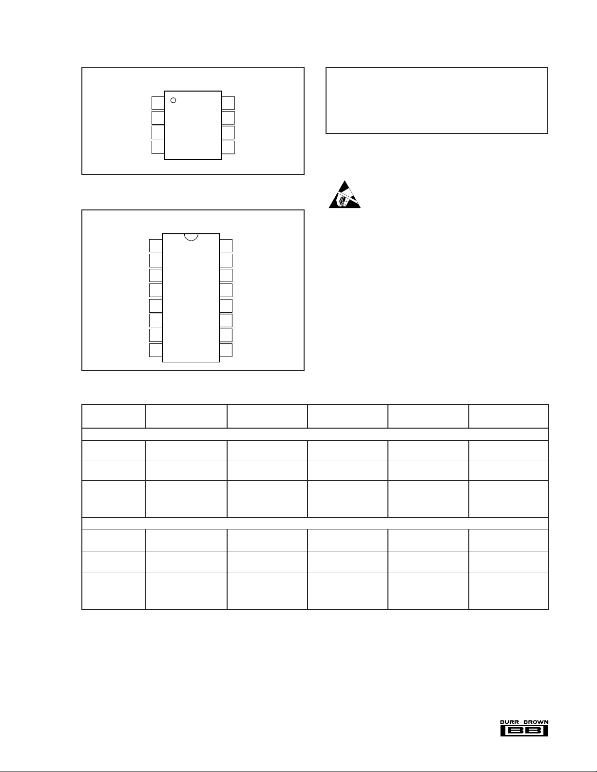
PIN CONFIGURATION (Single)
Top View 8-Pin DIP, SO-8, MSOP-8
1
R
G
–
2
V
IN
+
3
V
IN
4
V–
8
R
G
7
V+
6
V
O
5
Ref
PIN CONFIGURATION (Dual)
Top View 16-Pin DIP, SO-16, SSOP-16
V
V
R
R
Ref
V
Sense
–
INA
+
INA
V–
1
2
3
GA
4
GA
5
A
6
OA
7
A
8
–
16
V
INB
+
15
V
INB
14
R
GB
13
R
GB
12
Ref
B
11
V
OB
10
Sense
B
9
V+
ABSOLUTE MAXIMUM RATINGS
Power Supply Voltage, V+ to V– ........................................................ 36V
Input Signal Voltage
Input Signal Current
(2)
........................................... (V–)–0.7 to (V+)+0.7V
(2)
...................................................................... 10mA
(1)
Output Short Circuit ................................................................. Continuous
Operating Temperature ................................................. –55°C to +125°C
Storage Temperature ..................................................... –55°C to +125°C
Lead Temperature (soldering, 10s) ............................................... +300°C
NOTES: (1) Stresses above these ratings may cause permanent damage.
(2) Input signal voltage is limited by internal diodes connected to power
supplies. See text.
ELECTROSTATIC
DISCHARGE SENSITIVITY
This integrated circuit can be damaged by ESD. Burr-Brown
recommends that all integrated circuits be handled with appropriate precautions. Failure to observe proper handling and
installation procedures can cause damage.
ESD damage can range from subtle performance degradation
to complete device failure. Precision integrated circuits may
be more susceptible to damage because very small parametric
changes could cause the device not to meet its published
specifications.
PACKAGE INFORMATION
PRODUCT PACKAGE NUMBER
PACKAGE DRAWING TRANSPORT
Single
INA126PA 8-Pin DIP 006 INA126PA INA126PA Rails
INA126P 8-Pin DIP 006 INA126P INA126P Rails
INA126UA SO-8 182 INA126UA INA126UA Rails or Reel
INA126U SO-8 182 INA126U INA126U Rails or Reel
INA126EA
INA126E
(2)
" " " " INA126EA-2500 "
(2)
MSOP-8 337 A26
MSOP-8 337 A26
" " " " INA126E-2500 "
Dual
INA2126PA 16-Pin DIP 180 INA2126PA INA2126PA Rails
INA2126P 16-Pin DIP 180 INA2126P INA2126P Rails
INA2126UA SO-16 265 INA2126UA INA2126UA Rails
INA2126U SO-16 265 INA2126U INA2126U Rails
INA2126EA
INA2126E
(2)
" " " " INA2126EA-2500 "
(2)
SSOP-16 322 INA2126EA INA2126EA-250 Reel Only
SSOP-16 322 INA2126E INA2126E-250 Reel Only
" " " " INA2126E-2500 "
NOTES: (1) For detailed drawing and dimension table, see end of data sheet, or Appendix C of Burr-Brown IC Data Book. (2) MSOP-8 and SSOP-16 packages are
available only on 250 or 2500 piece reels. (3) Grade designation is marked on reel.
(1)
PACKAGE MARKING ORDERING NUMBER MEDIA
(3)
(3)
INA126EA-250 Reel Only
INA126E-250 Reel Only
®
3
INA126, INA2126
Page 4

TYPICAL PERFORMANCE CURVES
At TA = +25°C and VS = ±15V, unless otherwise noted.
70
G = 1000
60
GAIN vs FREQUENCY
50
G = 100
40
30
Gain (dB)
20
G = 20
G = 5
10
0
–10
100 1k 10k 100k 1M
Frequency (Hz)
POSITIVE POWER SUPPLY REJECTION
vs FREQUENCY
120
G = 1000
100
80
60
40
20
Power Supply Rejection (dB)
G = 5
G = 100
110
COMMON-MODE REJECTION vs FREQUENCY
100
90
80
70
G = 1000
60
50
G = 100
40
30
20
Common-Mode Rejection (dB)
10
0
10 100 1k 10k 100k 1M
Frequency (Hz)
NEGATIVE POWER SUPPLY REJECTION
vs FREQUENCY
120
100
80
G = 1000
60
40
20
Power Supply Rejection (dB)
G = 5
G = 5
G = 100
0
10 100 1k 10k 100k 1M
Frequency (Hz)
INPUT COMMON-MODE RANGE
15
vs OUTPUT VOLTAGE, V
output swing—see text
10
Limited by A
2
5
V
0
–5
Common-Mode Voltage (V)
–10
V
+
V
–15
+
D/2
–
+
D/2
–
CM
Limited by A
–15V
= ±15V
S
+15V
V
O
Ref
output swing—see text
2
–15 –10 0 5 15–5
Output Voltage (V)
®
INA126, INA2126
0
10 100 1k 10k 100k 1M
Frequency (Hz)
INPUT COMMON-MODE VOLTAGE RANGE
5
vs OUTPUT VOLTAGE, V
4
3
2
Limited by A
VS = ±5V
output swing—see text
2
1
0
= ±5V
S
VS = +5V/0V
V
= 2.5V
REF
–1
–2
–3
Input Common-Mode Voltage (V)
–4
Limited by A
output swing—see text
2
–5
10
–5 –4 5–3 –2 –1 0 1 2 3 4
Output Voltage (V)
4
Page 5

TYPICAL PERFORMANCE CURVES (CONT)
SETTLING TIME vs GAIN
Gain (V/V)
Settling Time (µs)
1000
100
10
1 10 100 1k
0.01%
0.1%
OUTPUT VOLTAGE SWING
vs OUTPUT CURRENT
012345
Output Current (mA)
Output Voltage (V)
Sourcing Current
Sinking Current
V+
(V+)–1
(V+)–2
(V–)+2
(V–)+1
V–
QUIESCENT CURRENT AND SLEW RATE
vs TEMPERATURE
Temperature (°C)
Quiescent Current (µA)
Slew Rate (V/µs)
300
250
200
150
100
50
0
0.6
0.5
0.4
0.3
0.2
0.1
0
–75 –50 –25 0 25 50 75 100 125
+SR
–SR
VS = ±5V
VS = ±1.35V
I
Q
At TA = +25°C and VS = ±15V, unless otherwise noted.
100
10
Input Voltage Noise (nV/√Hz)
1
10
–2
–4
–6
Offset Voltage Change (µV)
–8
–10
INPUT-REFERRED NOISE vs FREQUENCY
Voltage Noise
Current Noise
1 10 100 10k1k
Frequency (Hz)
INPUT-REFERRED OFFSET VOLTAGE WARM-UP
8
6
4
2
0
01 1023456789
Time After Turn-On (ms)
1k
100
Input Current Noise (fA/√Hz)
10
(Noise)
TOTAL HARMONIC DISTORTION+NOISE
1
0.1
THD+N (%)
0.01
0.001
10 100 1k
vs FREQUENCY
Frequency (Hz)
G = 5
RL = 10kΩ
RL = 100kΩ
10k
®
5
INA126, INA2126
Page 6

TYPICAL PERFORMANCE CURVES (CONT)
At TA = +25°C and VS = ±15V, unless otherwise noted.
SMALL-SIGNAL RESPONSE, G = 5
20mV/div
5V/div
50µs/div
SMALL-SIGNAL RESPONSE, G = 100
20mV/div
50µs/div
VOLTAGE NOISE, 0.1Hz to 10HzLARGE-SIGNAL RESPONSE, G = 5
0.2µV/div
50µs/div
®
INA126, INA2126
CHANNEL SEPARATION vs FREQUENCY, RTI
160
150
140
130
120
110
100
Separation (dB)
RL = 25kΩ
90
80
70
60
100 1k 10k 100k 1M
Measurement limited
by amplifier or
measurement noise.
(Dual Version)
G = 100
G = 5
Frequency (Hz)
6
500ms/div
G = 1000
Page 7

APPLICATION INFORMATION
10kΩ
OPA237
±10mV
Adjustment Range
100Ω
100Ω
100µA
1/2 REF200
100µA
1/2 REF200
V+
V–
R
G
INA126
Ref
V
O
✻
V
IN
–
V
IN
+
✻ Dual version has
external sense connection.
Figure 1 shows the basic connections required for operation
of the INA126. Applications with noisy or high impedance
power supplies may require decoupling capacitors close to
the device pins as shown.
The output is referred to the output reference (Ref) terminal
which is normally grounded. This must be a low-impedance
connection to ensure good common-mode rejection. A resistance of 8Ω in series with the Ref pin will cause a typical
device to degrade to approximately 80dB CMR.
Dual versions (INA2126) have feedback sense connections,
and SenseB. These must be connected to their respec-
Sense
A
tive output terminals for proper operation. The sense connection can be used to sense the output voltage directly at the
load for best accuracy.
SETTING THE GAIN
Gain is set by connecting an external resistor, R
, as shown:
G
equation (1). Low resistor values required for high gain can
make wiring resistance important. Sockets add to the wiring
resistance, which will contribute additional gain error in
gains of approximately 100 or greater.
OFFSET TRIMMING
The INA126 and INA2126 are laser trimmed for low offset
voltage and offset voltage drift. Most applications require no
external offset adjustment. Figure 2 shows an optional circuit for trimming the output offset voltage. The voltage
applied to the Ref terminal is added to the output signal. An
op amp buffer is used to provide low impedance at the Ref
terminal to preserve good common-mode rejection.
G =5+
80kΩ
Commonly used gains and R
R
G
resistor values are shown in
G
(1)
Figure 1.
The 80kΩ term in equation 1 comes from the internal metal film
resistors which are laser trimmed to accurate absolute values.
The accuracy and temperature coefficient of these resistors are
included in the gain accuracy and drift specifications.
The stability and temperature drift of the external gain
setting resistor, R
, also affects gain. RG’s contribution to
G
gain accuracy and drift can be directly inferred from the gain
DESIRED GAIN RGNEAREST 1%
(V/V) (Ω)R
5NCNC
10 16k 15.8k
20 5333 5360
50 1779 1780
100 842 845
200 410 412
500 162 162
1000 80.4 80.6
2000 40.1 40.2
5000 16.0 15.8
10000 8.0 7.87
NC: No Connection.
FIGURE 1. Basic Connections.
Also drawn in simplified form:
VALUE
G
+
V
IN
R
–
V
IN
INA126
G
✻
Ref
FIGURE 2. Optional Trimming of Output Offset Voltage.
V+
Pin numbers are
for single version
3
+
V
IN
8
R
G
1
–
V
IN
2
V
O
✻ Dual version has
external sense connection.
7
0.1µF
7
INA126
A
1
10kΩ
A
2
V–
4
40kΩ
10kΩ
40kΩ
0.1µF
6
✻
5
Ref
INA126, INA2126
G = 5 +
VO = (VIN – VIN) G
Load
80k
R
G
–+
+
V
O
–
®
Page 8

INPUT BIAS CURRENT RETURN
The input impedance of the INA126/2126 is extremely
high—approximately 10
9
Ω. However, a path must be pro-
vided for the input bias current of both inputs. This input
bias current is typically –10nA (current flows out of the
input terminals). High input impedance means that this input
bias current changes very little with varying input voltage.
Input circuitry must provide a path for this input bias current
for proper operation. Figure 3 shows various provisions for
an input bias current path. Without a bias current path, the
inputs will float to a potential which exceeds the commonmode range and the input amplifiers will saturate.
If the differential source resistance is low, the bias current
return path can be connected to one input (see the thermocouple example in Figure 3). With higher source impedance,
using two equal resistors provides a balanced input with
advantages of lower input offset voltage due to bias current
and better high-frequency common-mode rejection.
Microphone,
Hydrophone
etc.
INA126
The internal op amp A2 is identical to A1 and its output
swing is limited to typically 0.7V from the supply rails.
When the input common-mode range is exceeded (A2’s
output is saturated), A1 can still be in linear operation and
respond to changes in the non-inverting input voltage. The
output voltage, however, will be invalid.
LOW VOLTAGE OPERATION
The INA126/2126 can be operated on power supplies as low
as ±1.35V. Performance remains excellent with power supplies ranging from ±1.35V to ±18V. Most parameters vary
only slightly throughout this supply voltage range—see
typical performance curves. Operation at very low supply
voltage requires careful attention to ensure that the commonmode voltage remains within its linear range. See “Input
Common-Mode Voltage Range.”
The INA126/2126 can be operated from a single power
supply with careful attention to input common-mode range,
output voltage swing of both op amps and the voltage
applied to the Ref terminal. Figure 4 shows a bridge amplifier circuit operated from a single +5V power supply. The
bridge provides an input common-mode voltage near 2.5V,
with a relatively small differential voltage.
47kΩ47kΩ
Thermocouple
10kΩ
Center-tap provides
bias current return.
INA126
INA126
FIGURE 3. Providing an Input Common-Mode Current Path.
INPUT COMMON-MODE RANGE
The input common-mode range of the INA126/2126 is
shown in typical performance curves. The common-mode
range is limited on the negative side by the output voltage
swing of A
, an internal circuit node that cannot be measured
2
on an external pin. The output voltage of A2 can be expressed as:
= 1.25 VIN – (VIN – VIN) (10kΩ/RG) (2)
V
O2
–+–
(Voltages referred to Ref terminal, pin 5)
INPUT PROTECTION
The inputs are protected with internal diodes connected to
the power supply rails. These diodes will clamp the applied
signal to prevent it from exceeding the power supplies by
more than approximately 0.7V. If the signal source voltage
can exceed the power supplies, the source current should be
limited to less than 10mA. This can generally be done with
a series resistor. Some signal sources are inherently currentlimited and do not require limiting resistors.
CHANNEL CROSSTALK—DUAL VERSION
The two channels of the INA2126 are completely independent, including all bias circuitry. At DC and low frequency
there is virtually no signal coupling between channels.
Crosstalk increases with frequency and is dependent on
circuit gain, source impedance and signal characteristics.
As source impedance increases, careful circuit layout will
help achieve lowest channel crosstalk. Most crosstalk is
produced by capacitive coupling of signals from one channel
to the input section of the other channel. To minimize
coupling, separate the input traces as far as practical from
any signals associated with the opposite channel. A grounded
guard trace surrounding the inputs helps reduce stray coupling between channels. Carefully balance the stray capacitance of each input to ground, and run the differential inputs
of each channel parallel to each other, or directly adjacent on
top and bottom side of a circuit board. Stray coupling then
tends to produce a common-mode signal that is rejected by
the IA’s input.
®
INA126, INA2126
8
Page 9

+5V
The ADS7817’s V
conversion rate 10kS/s or slower assures enough current to turn on the
input current is proportional to conversion rate. A
REF
reference diode. Converter input range is ±1.2V. Output swing limitation of
INA126 limits the A/D converter to somewhat greater than 11 bits of range.
7
INA126
A
1
10kΩ
A
2
40k
10kΩ
40kΩ
Ω
Bridge
Sensor
2.5V + ∆V
2.5V – ∆V
R
3
8
G
1
2
4
A similar instrumentation amplifier, INA125, provides
an internal reference voltage for sensor excitation
and/or A/D converter reference.
FIGURE 4. Bridge Signal Acquisition—Single 5V Supply.
6
5
✻
1.2V
68
4
R
, C1, R2:
1
340Hz LP
R
1
1kΩ
C
1
0.47µF
R
2
1kΩ
33µA
REF1004C-1.2
8
2
+IN
ADS7817
3
–IN
12-Bit
A/D
1
V
REF
4
✻ Dual version has external
sense connection. Pin numbers
shown are for single version.
INA126 and ADS7817
are available in fine-pitch
MSOP-8 package
6
Serial
Data
5
Chip
Select
7
Clock
C
Ck
D
S
A
1
IB Error
OPA177 ±1.5nA
OPA130 ±20pA
OPA602 ±1pA
OPA129 ±100fA
FIGURE 5. Differential Voltage-to-Current Converter.
–
V
IN
+
R
INA126
G
✻
Ref
R
1
I
B
A
1
V
I
= • G
O
IN
R
1
I
O
Load
✻ Dual version has external sense connection.
®
9
INA126, INA2126
 Loading...