

Burr Brown INA122UA-2K5, INA122UA, INA122U-2K5, INA122PA, INA122P Datasheet
...
©1997 Burr-Brown Corporation PDS-1388B Printed in U.S.A. October, 1997
100kΩ
25kΩ
25kΩ
100kΩ
INA122
5
4
2
1
8
3
7
6
R
G
V
IN
–
V
IN
+
V+
V
O
Ref
V–
200k
R
G
G = 5 +
V
O
= (VIN – VIN) G
–+
®
INA122
Single Supply,
Micro
Power
INSTRUMENTATION AMPLIFIER
FEATURES
● LOW QUIESCENT CURRENT: 60µA
● WIDE POWER SUPPLY RANGE
Single Supply: 2.2V to 36V
Dual Supply: –0.9/+1.3V to
±18V
● COMMON-MODE RANGE TO (V–)–0.1V
● RAIL-TO-RAIL OUTPUT SWING
● LOW OFFSET VOLTAGE: 250
µV max
● LOW OFFSET DRIFT: 3
µV/°C max
● LOW NOISE: 60nV/√Hz
● LOW INPUT BIAS CURRENT: 25nA max
● 8-PIN DIP AND SO-8 SURFACE-MOUNT
APPLICATIONS
● PORTABLE, BATTERY OPERATED
SYSTEMS
● INDUSTRIAL SENSOR AMPLIFIER:
Bridge, RTD, Thermocouple
● PHYSIOLOGICAL AMPLIFIER:
ECG, EEG, EMG
● MULTI-CHANNEL DATA ACQUISITION
INA122
INA122
International Airport Industrial Park • Mailing Address: PO Box 11400, Tucson, AZ 85734 • Street Address: 6730 S. Tucson Blvd., Tucson, AZ 85706 • Tel: (520) 746-1111 • Twx: 910-952-1111
Internet: http://www.burr-brown.com/ • FAXLine: (800) 548-6133 (US/Canada Only) • Cable: BBRCORP • Telex: 066-6491 • FAX: (520) 889-1510 • Immediate Product Info: (800) 548-6132
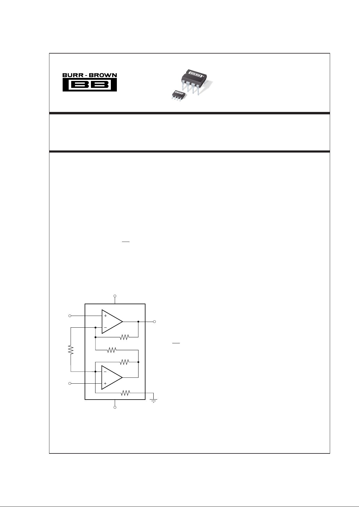
DESCRIPTION
The INA122 is a precision instrumentation amplifier
for accurate, low noise differential signal acquisition.
Its two-op-amp design provides excellent performance
with very low quiescent current, and is ideal for
portable instrumentation and data acquisition systems.
The INA122 can be operated with single power supplies from 2.2V to 36V and quiescent current is a mere
60µA. It can also be operated from dual supplies. By
utilizing an input level-shift network, input commonmode range extends to 0.1V below negative rail (single
supply ground).
A single external resistor sets gain from 5V/V to
10000V/V. Laser trimming provides very low offset
voltage (250µV max), offset voltage drift (3µV/°C
max) and excellent common-mode rejection.
Package options include 8-pin plastic DIP and SO-8
surface-mount packages. Both are specified for the
–40°C to +85°C extended industrial temperature range.
2
®
INA122
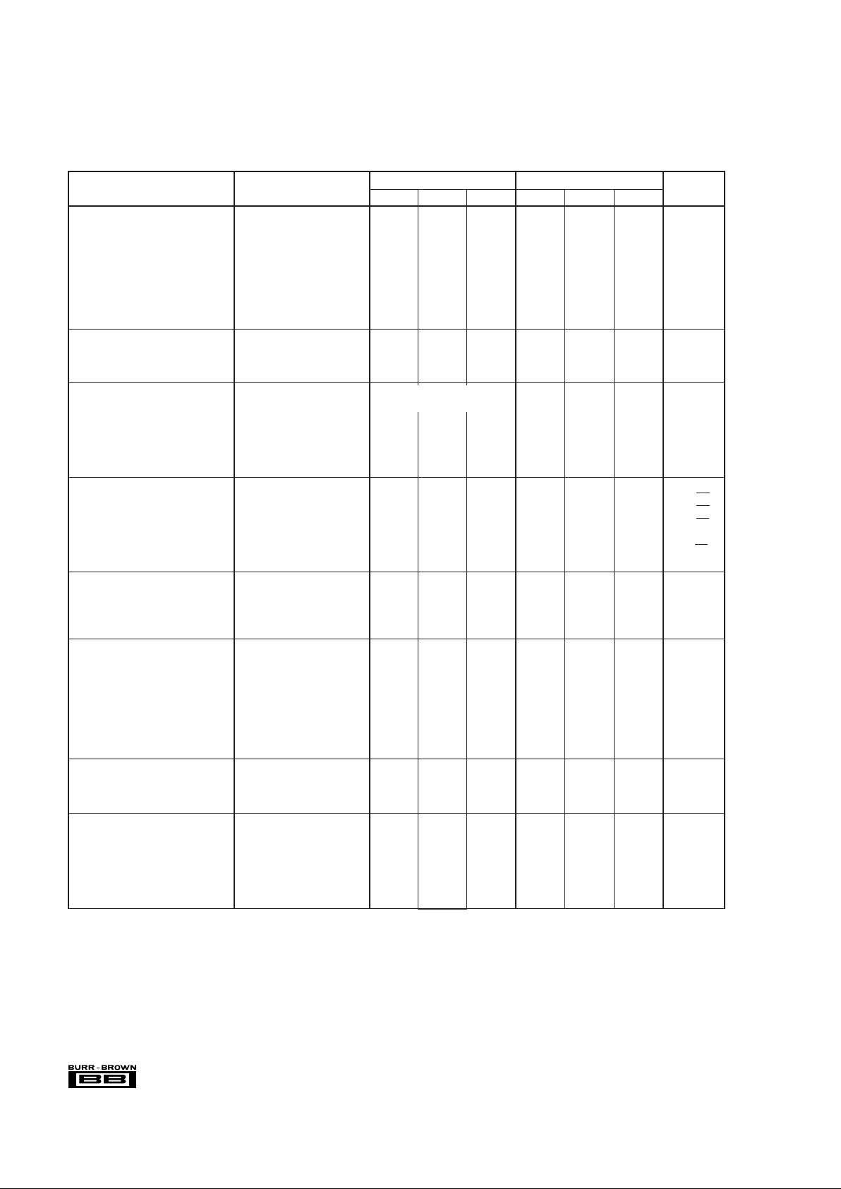
SPECIFICATIONS
At TA = +25°C, VS = +5V, RL = 20kΩ connected to VS/2, unless otherwise noted.
The information provided herein is believed to be reliable; however, BURR-BROWN assumes no responsibility for inaccuracies or omissions. BURR-BROWN assumes
no responsibility for the use of this information, and all use of such information shall be entirely at the user’s own risk. Prices and specifications are subject to change
without notice. No patent rights or licenses to any of the circuits described herein are implied or granted to any third party. BURR-BROWN does not authorize or warrant
any BURR-BROWN product for use in life support devices and/or systems.
INA122P, U INA122PA, UA
PARAMETER CONDITIONS MIN TYP MAX MIN TYP MAX UNITS
INPUT
Offset Voltage, RTI ±100 ±250 ±150 ±500 µV
vs Temperature ±1 ±3 ✻ ±5 µV/°C
vs Power Supply (PSRR) V
S
= +2.2V to +36V 10 30 ✻ 100 µV/V
Input Impedance 10
10
|| 3 ✻ Ω || pF
Safe Input Voltage R
S
= 0 (V–)–0.3 (V+)+0.3 ✻✻V
R
S
= 10kΩ (V–)–40 (V+)+40 ✻✻V
Common-Mode Voltage Range 0 3.4 ✻✻V
Common-Mode Rejection V
CM
= 0V to 3.4V 83 96 76 90 dB
INPUT BIAS CURRENT –10 –25 ✻ –50 nA
vs Temperature ±40 ✻ pA/°C
Offset Current ±1 ±2 ✻ ±5nA
vs Temperature ±40 ✻ pA/°C
GAIN G = 5 to 10k ✻ V/V
Gain Equation G = 5 + 200kΩ/R
G
✻ V/V
Gain Error G = 5 ±0.05 ±0.1 ✻ ±0.15 %
vs Temperature G = 5 5 10 ✻✻ppm/°C
Gain Error G = 100 ±0.3 ±0.5 ✻ ±1%
vs Temperature G = 100 ±25 ±100 ✻✻ppm/°C
Nonlinearity
G = 100, VO = –14.85V to +14.9V
±0.005 ±0.012 ✻ ±0.024 %
NOISE (RTI)
Voltage Noise, f = 1kHz 60 ✻ nV/√Hz
f = 100Hz 100 ✻ nV/√Hz
f = 10Hz 110 ✻ nV/√Hz
f
B
= 0.1Hz to 10Hz 2 ✻ µVp-p
Current Noise, f = 1kHz 80 ✻ fA/√Hz
f
B
= 0.1Hz to 10Hz 2 ✻ pAp-p
OUTPUT
Voltage, Positive V
S
= ±15V (V+)–0.1 (V+)–0.05 ✻✻ V
Negative V
S
= ±15V (V–)+0.15 (V–)+0.1 ✻✻ V
Short-Circuit Current Short-Circuit to Ground +3/–30 ✻ mA
Capacitive Load Drive 1 ✻ nF
FREQUENCY RESPONSE
Bandwidth, –3dB G = 5 120 ✻ kHz
G = 100 5 ✻ kHz
G = 500 0.9 ✻ kHz
Slew Rate
+0.08/–0.16
✻ V/µs
Settling Time, 0.01% G = 5 350 ✻ µs
G = 100 450 ✻ µs
G = 500 1.8 ✻ ms
Overload Recovery 50% Input Overload 3 ✻ µs
POWER SUPPLY
Voltage Range, Single Supply +2.2 +5 +36 ✻✻✻ V
Dual Supplies –0.9/+1.3 ±18 ✻✻✻ V
Current I
O
= 0 60 8 5 ✻✻ µA
TEMPERATURE RANGE
Specification –40 +85 ✻✻°C
Operation –55 +85 ✻✻°C
Storage –55 +125 ✻✻°C
Thermal Resistance,
θ
JA
8-Pin DIP 150 ✻ °C/W
SO-8 Surface-Mount 150 ✻ °C/W
✻ Specification same as INA122P, INA122U.
3
®
INA122
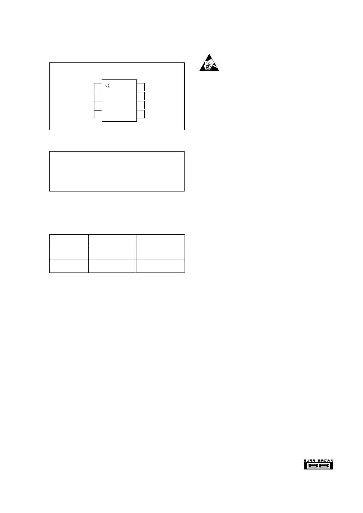
PIN CONFIGURATION
Top View 8-Pin DIP, SO-8
Supply Voltage, V+ to V– .................................................................... 36V
Signal Input Terminals, Voltage
(2)
....................... (V–)–0.3V to (V+)+0.3V
Current
(2)
...................................................... 5mA
Output Short Circuit ................................................................. Continuous
Operating Temperature ................................................. –40°C to +125°C
Storage Temperature ..................................................... –55°C to +125°C
Lead Temperature (soldering, 10s)............................................... +300°C
NOTES: (1) Stresses above these ratings may cause permanent damage.
(2) Input terminals are internally diode-clamped to the power supply rails.
Input signals that can exceed the supply rails by more than 0.3V should be
current-limited to 5mA or less.
ABSOLUTE MAXIMUM RATINGS
(1)
PACKAGE INFORMATION
PACKAGE DRAWING
PRODUCT PACKAGE NUMBER
(1)
INA122PA 8-Pin DIP 006
INA122P 8-Pin DIP 006
INA122UA SO-8 Surface Mount 182
INA122U SO-8 Surface Mount 182
NOTE: (1) For detailed drawing and dimension table, see end of data sheet, or
Appendix C of Burr-Brown IC Data Book.
ELECTROSTATIC
DISCHARGE SENSITIVITY
This integrated circuit can be damaged by ESD. Burr-Brown
recommends that all integrated circuits be handled with appropriate precautions. Failure to observe proper handling and
installation procedures can cause damage.
ESD damage can range from subtle performance degradation
to complete device failure. Precision integrated circuits may
be more susceptible to damage because very small parametric
changes could cause the device not to meet its published
specifications.
R
G
V
IN
V
IN
V–
R
G
V+
V
O
Ref
1
2
3
4
8
7
6
5
–
+
 Loading...