

Burr Brown INA117SMQ, INA117SM, INA117KU-2K5, INA117KU, INA117BM Datasheet
...
INA117
FEATURES
● COMMON-MODE INPUT RANGE:
±200V (V
S
= ±15V)
● PROTECTED INPUTS:
±500V Common-Mode
±500V Differential
● UNITY GAIN: 0.02% Gain Error max
● NONLINEARITY: 0.001% max
● CMRR: 86dB min
APPLICATIONS
● CURRENT MONITOR
● BATTERY CELL-VOLTAGE MONITOR
● GROUND BREAKER
● INPUT PROTECTION
● SIGNAL ACQUISITION IN NOISY
ENVIRONMENTS
● FACTORY AUTOMATION
DESCRIPTION
The INA117 is a precision unity-gain difference
amplifier with very high common-mode input voltage
range. It is a single monolithic IC consisting of a
precision op amp and integrated thin-film resistor
network. It can accurately measure small differential
voltages in the presence of common-mode signals up
to ±200V. The INA117 inputs are protected from
momentary common-mode or differential overloads
up to ±500V.
In many applications, where galvanic isolation is not
essential, the INA117 can replace isolation amplifiers.
This can eliminate costly isolated input-side power
supplies and their associated ripple, noise and quiescent current. The INA117’s 0.001% nonlinearity and
200kHz bandwidth are superior to those of conventional isolation amplifiers.
The INA117 is available in 8-pin plastic mini-DIP and
SO-8 surface-mount packages, specified for the –40°C
to +85°C temperature range. The metal TO-99 models
are available specified for the –40°C to +85°C and
–55°C to +125°C temperature range.
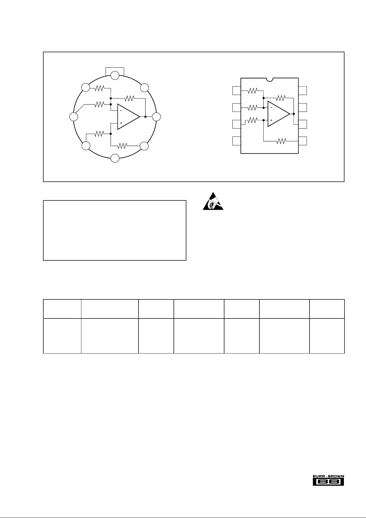
®
High Common-Mode Voltage
DIFFERENCE AMPLIFIER
Ref
B
–In
+In
V–
Comp
V+
V
O
Ref
A
1
2
3
4
8
7
6
5
21.11kΩ
380kΩ
380kΩ
380kΩ
20kΩ
International Airport Industrial Park • Mailing Address: PO Box 11400, Tucson, AZ 85734 • Street Address: 6730 S. Tucson Blvd., Tucson, AZ 85706 • Tel: (520) 746-1111
Twx: 910-952-1111 • Internet: http://www.burr-brown.com/ • Cable: BBRCORP • Telex: 066-6491 • FAX: (520) 889-1510 • Immediate Product Info: (800) 548-6132
INA117
INA117
© 1987 Burr-Brown Corporation PDS-748G Printed in U.S.A. August, 1999

2
®
INA117
SPECIFICATIONS
ELECTRICAL
At TA = +25°C, VS = ±15V, unless otherwise noted.
INA117AM, SM INA117BM INA117P, KU
PARAMETER CONDITIONS MIN TYP MAX MIN TYP MAX MIN TYP MAX UNITS
GAIN
Initial
(1)
1 ✻✻V/V
Error 0.01 0.05 ✻ 0.02 ✻✻ %
vs Temperature 2 10 ✻✻ppm/°C
Nonlinearity
(2)
0.0002 0.001 ✻✻ ✻✻ %
OUTPUT
Rated Voltage I
O
= +20mA, –5mA 10 12 ✻✻ ✻✻ V
Rated Current V
O
= 10V +20, –5 ✻✻mA
Impedance 0.01 ✻✻Ω
Current Limit To Common +49, –13 ✻✻mA
Capacitive Load Stable Operation 1000 ✻✻pF
INPUT
Impedance Differential 800 ✻✻kΩ
Common-Mode 400 ✻✻kΩ
Voltage Range Differential ±10 ✻✻V
Common-Mode, Continuous
±200 ✻✻V
Common-Mode Rejection
(3)
DC 70 80 86 94 ✻✻ dB
AC, 60Hz V
CM
= 400Vp-p 66 80 66 94 ✻✻ dB
vs Temperature, DC T
A
= T
MIN
to T
MAX
AM, BM, P, KU 66 75 80 90 ✻ dB
SM 60 75 dB
OFFSET VOLTAGE RTO
(4)
Initial 120 1000 ✻ 1000 ✻✻µV
KU Grade (SO-8 Package) 600 2000 µV
vs Temperature T
A
= T
MIN
to T
MAX
8.5 40 ✻ 20 ✻ µV/°C
vs Supply V
S
= ±5V to ±18V 74 90 80 ✻✻✻dB
vs Time 200 ✻✻µV/mo
OUTPUT NOISE VOLTAGE RTO
(5)
fB = 0.01Hz to 10Hz 25 ✻✻µVp-p
f
B
= 10kHz 550 ✻✻nV/√Hz
DYNAMIC RESPONSE
Gain Bandwidth, –3dB 200 ✻✻kHz
Full Power Bandwidth V
O
= 20Vp-p 30 ✻✻kHz
Slew Rate 2 2.6 ✻✻ ✻✻ V/µs
Settling Time: 0.1% V
O
= 10V Step 6.5 ✻✻µs
0.01% V
O
= 10V Step 10 ✻✻µs
0.01% V
CM
= 10V Step, V
DIFF
= 0V 4.5 ✻✻µs
POWER SUPPLY
Rated ±15 ✻✻V
Voltage Range Derated Performance ±5 ±18 ✻✻✻✻V
Quiescent Current V
O
= 0V 1.5 2 ✻✻ ✻✻mA
TEMPERATURE RANGE
Specification: AM, BM, P, KU –25 +85 ✻✻–40 +85 °C
SM –55 +125 °C
Operation –55 +125 ✻✻–40 +85 °C
Storage –65 +150 ✻✻–55 +125 °C
✻Specification same as for INA117AM.
NOTES: (1) Connected as difference amplifier (see Figure 1). (2) Nonlinearity is the maximum peak deviation from the best-fit straight line as a percent of full-scale
peak-to-peak output. (3) With zero source impedance (see discussion of common-mode rejection in Application Information section). (4) Includes effects of amplifier’s
input bias and offset currents. (5) Includes effects of amplifier’s input current noise and thermal noise contribution of resistor network.
The information provided herein is believed to be reliable; however, BURR-BROWN assumes no responsibility for inaccuracies or omissions. BURR-BROWN assumes
no responsibility for the use of this information, and all use of such information shall be entirely at the user’s own risk. Prices and specifications are subject to change
without notice. No patent rights or licenses to any of the circuits described herein are implied or granted to any third party. BURR-BROWN does not authorize or warrant
any BURR-BROWN product for use in life support devices and/or systems.
3
INA117
®
Ref
B
–In
+In
V–
Comp
V+
Output
Ref
A
1
2
3
4
8
7
6
5
8
7
62
1
3
4
5
Tab
Comp
Output
V+
V–
Ref A
Ref B
–In
+In
Case internally connected to V–. Make no connection.
PIN CONFIGURATION
Top View TO-99
INA117AM, BM, SM
Top View DIP/SOIC
INA117P, KU
PACKAGE SPECIFIED
DRAWING TEMPERATURE PACKAGE ORDERING TRANSPORT
PRODUCT PACKAGE NUMBER
(1)
RANGE MARKING NUMBER
(2)
MEDIA
INA117P 8-Pin Plastic DIP 006 –40
°C to +85°C
INA117KU SO-8 Surface-Mount 182 "
INA117AM TO-99 Metal 001 –25°C to +85°C
INA117BM " " "
INA117SM " " –55°C to +125°C
NOTES: (1) For detailed drawing and dimension table, please see end of data sheet, or Appendix C of Burr-Brown IC Data Book. (2) Models with a slash (/ )
are available only in Tape and Reel in the quantities indicated (e.g., /2K5 indicates 2500 devices per reel). Ordering 2500 pieces of “INA117KU/2K5” will get a
single 2500-piece Tape and Reel. For detailed Tape and Reel mechanical information, refer to Appendix B of Burr-Brown IC Data Book.
PACKAGE/ORDERING INFORMATION
ELECTROSTATIC
DISCHARGE SENSITIVITY
This integrated circuit can be damaged by ESD. Burr-Brown
recommends that all integrated circuits be handled with
appropriate precautions. Failure to observe proper handling
and installation procedures can cause damage.
ESD damage can range from subtle performance degradation to complete device failure. Precision integrated circuits
may be more susceptible to damage because very small
parametric changes could cause the device not to meet its
published specifications.
ABSOLUTE MAXIMUM RATINGS
Supply Voltage .................................................................................. ±22V
Input Voltage Range, Continuous ................................................... ±200V
Common-Mode and Differential, 10s ........................................... ±500V
Operating Temperature
M Metal TO-99 ................................................................ –55 to +125 °C
P Plastic DIP and U SO-8 ................................................–40 to +85°C
Storage Temperature
M Package .......................................................................–65 to +150°C
P Plastic DIP and U SO-8 ..............................................–55 to +125°C
Lead Temperature (soldering, 10s) ............................................... +300 °C
Output Short Circuit to Common ............................................ Continuous
4
®
INA117
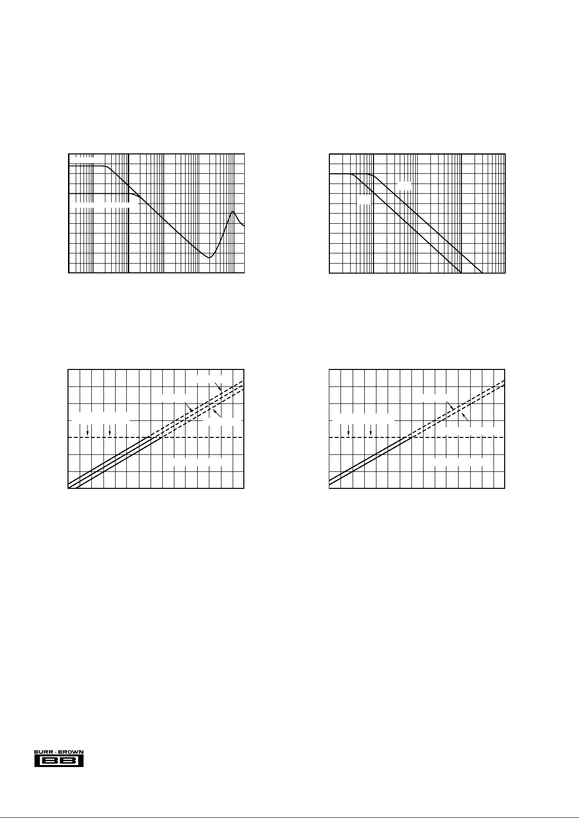
TYPICAL PERFORMANCE CURVES
At TA = +25°C, VS = ±15V, unless otherwise noted.
POSITIVE COMMON-MODE VOLTAGE RANGE
vs POSITIVE POWER SUPPLY VOLTAGE
Positive Power Supply Voltage (V)
5101520
400
350
300
250
200
150
100
50
Positive Common-Mode Range (V)
TA = +25°C
TA = –55°C
TA = +125°C
–VS = –5V to –20V
Max Rating = 200V
NEGATIVE COMMON-MODE VOLTAGE RANGE
vs NEGATIVE POWER SUPPLY VOLTAGE
Negative Power Supply Voltage (V)
–5 –10 –15 –20
–400
–350
–300
–250
–200
–150
–100
–50
Negative Common-Mode Range (V)
TA = +25°C
TA = –55°C to +125°C
+VS = +5V to +20V
Max Rating = –200V
POWER SUPPLY REJECTION vs FREQUENCY
Frequency (Hz)
1 10 100 1k 10k
100
90
80
70
60
50
40
Power Supply Rejection (dB)
V+
V–
COMMON-MODE REJECTION vs FREQUENCY
Frequency (Hz)
20 100 1k 10k 100k 2M
100
90
80
70
60
50
40
Common-Mode Rejection (dB)
INA117AM, SM, P, KU
INA117BM
5
INA117
®
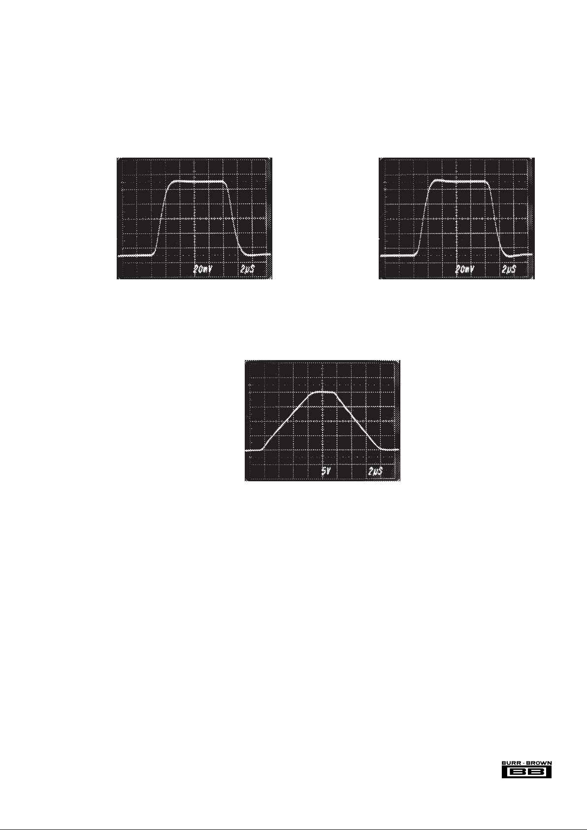
TYPICAL PERFORMANCE CURVES (CONT)
At TA = +25°C, VS = ±15V, unless otherwise noted.
SMALL SIGNAL STEP RESPONSE
CL = 1000pF
SMALL SIGNAL STEP RESPONSE
CL = 0
LARGE SIGNAL STEP RESPONSE
 Loading...