

Burr Brown INA116UA, INA116PA Datasheet
INA116
INA116
®
Ultra Low Input Bias Current
INSTRUMENTATION AMPLIFIER
INA1 16
FEATURES
● LOW INPUT BIAS CURRENT: 3fA typ
● BUFFERED GUARD DRIVE PINS
● LOW OFFSET VOLTAGE: 2mV max
● HIGH COMMON-MODE REJECTION:
84dB (G = 10)
● LOW QUIESCENT CURRENT: 1mA
● INPUT OVER-VOLTAGE PROTECTION:
APPLICATIONS
● LABORATORY INSTRUMENTATION
● pH MEASUREMENT
● ION–SPECIFIC PROBES
● LEAKAGE CURRENT MEASUREMENT
Guard
Guard
2
–
3
V
IN
Over-Voltage
4
1
Protection
+1
±40V
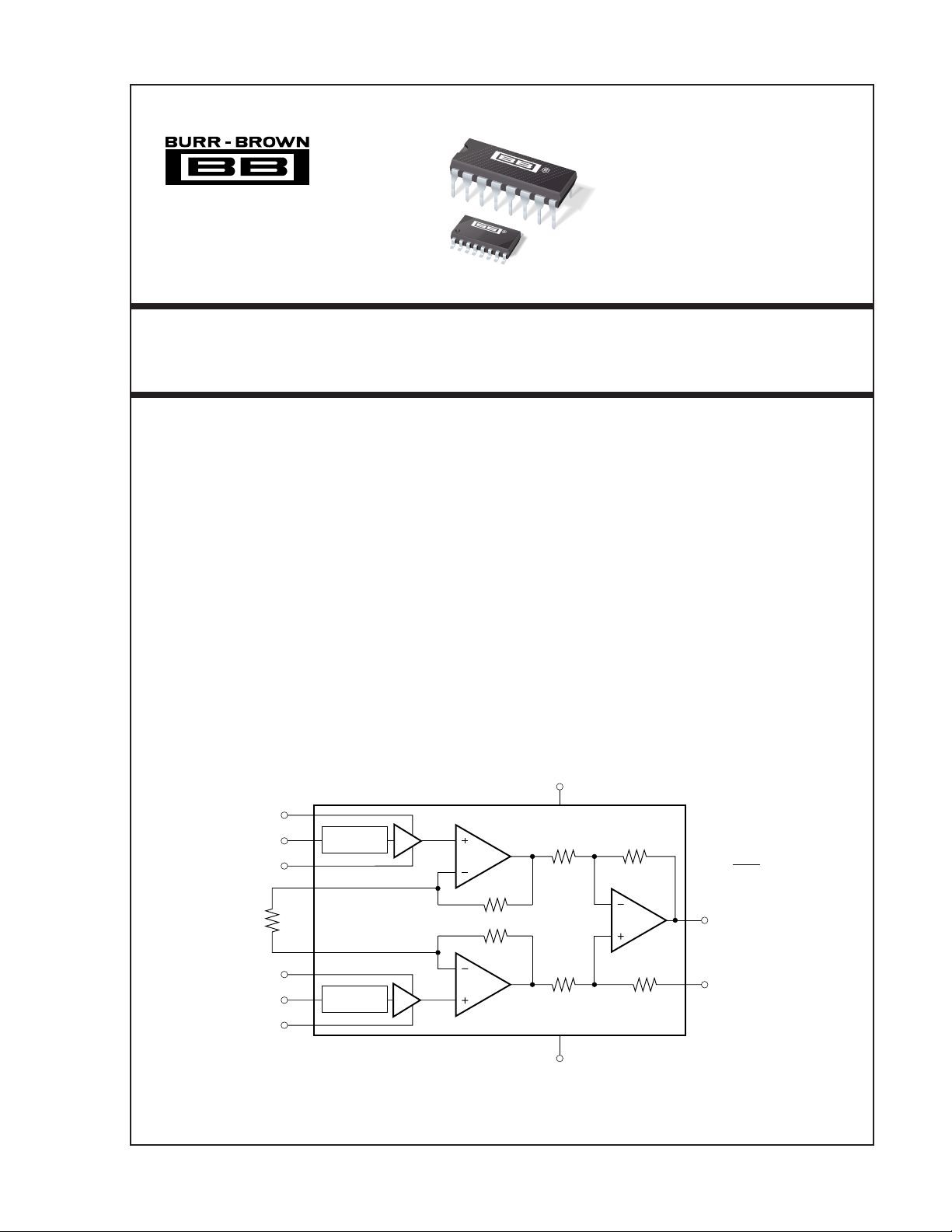
DESCRIPTION
The INA116 is a complete monolithic FET-input instrumentation amplifier with extremely low input bias
current.
yield input bias currents of 3fA at 25°C, and only 25fA
at 85°C. Its 3-op amp topology allows gains to be set
from 1 to 1000 by connecting a single external resistor.
Guard pins adjacent to both input connections can be
used to drive circuit board and input cable guards to
maintain extremely low input bias current.
The INA116 is available in 16-pin plastic DIP and SOL-16
surface-mount packages, specified for the –40°C to +85°C
temperature range.
V+
A
1
25kΩ
®
Difet
inputs and special guarding techniques
13
INA116
50kΩ
60kΩ60kΩ
G = 1 +
R
G
R
G
16
Guard
Guard
®
Difet
; Burr-Brown Corporation
International Airport Industrial Park • Mailing Address: PO Box 11400, Tucson, AZ 85734 • Street Address: 6730 S. Tucson Blvd., Tucson, AZ 85706 • Tel: (520) 746-1111 • Twx: 910-952-1111
Internet: http://www.burr-brown.com/ • FAXLine: (800) 548-6133 (US/Canada Only) • Cable: BBRCORP • Telex: 066-6491 • FAX: (520) 889-1510 • Immediate Product Info: (800) 548-6132
5
+
6
V
IN
Over-Voltage
7
Protection
+1
25kΩ
A
2
8
V–
A
3
60kΩ60kΩ
V
O
11
Ref
9
©1994 Burr-Brown Corporation PDS-1242B Printed in U.S.A. May, 1995
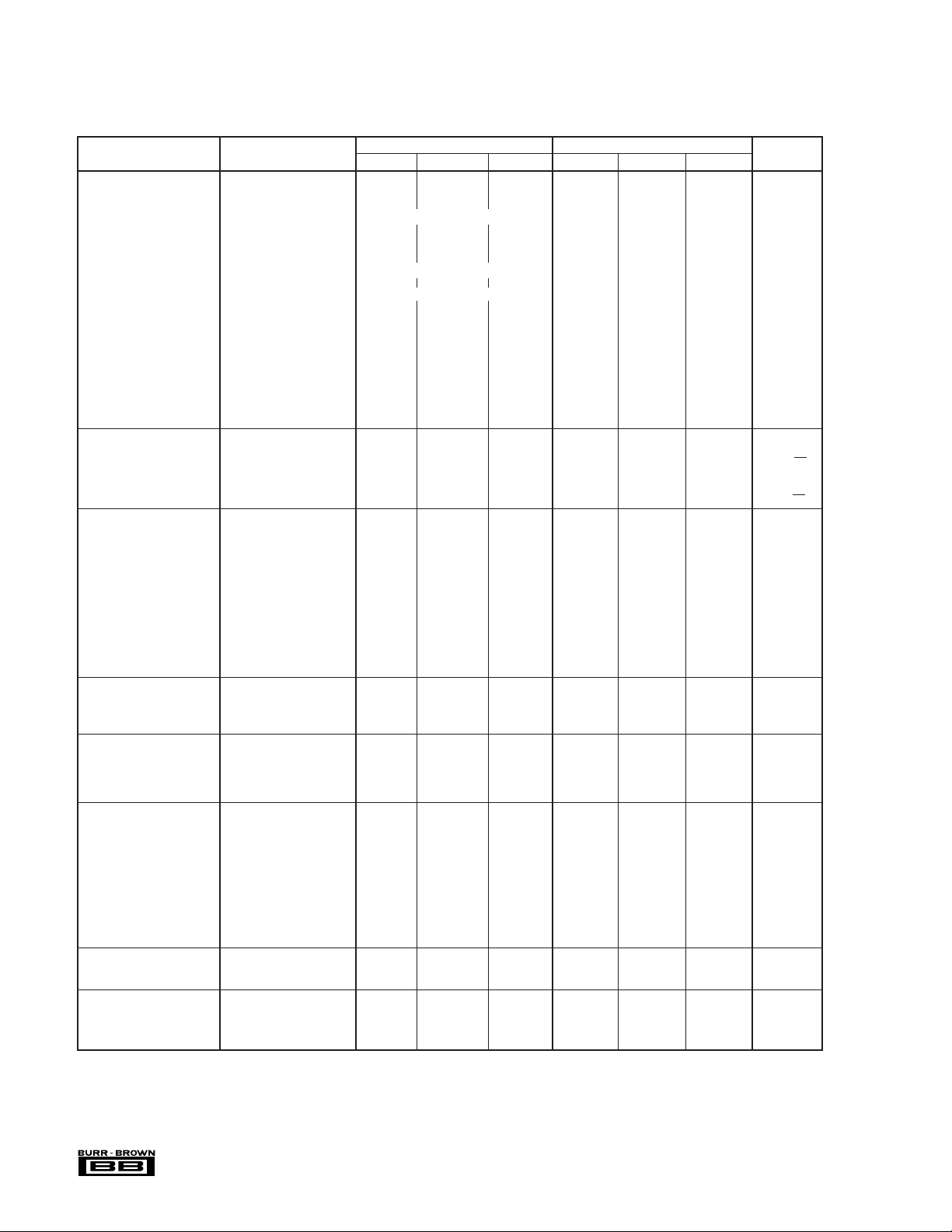
SPECIFICATIONS
AT TA = +25°C, VS = ±15V, RL = 10kΩ, unless otherwise noted.
INA116P, U INA116PA, UA
PARAMETER CONDITIONS MIN TYP MAX MIN TYP MAX UNITS
INPUT
Offset Voltage, RTI
Initial T
vs Temperature T
vs Power Supply V
Long-Term Stability ±1 ±5/G ✻ µV/mo
Bias Current ±3 ±25 ✻ ±100 fA
vs Temperature See Typical Curve ✻
Offset Current ±1 ±25 ✻ ±100 fA
vs Temperature See Typical Curve ✻
Impedance, Differential >10
Common-Mode >10
Common-Mode Voltage Range
Safe Input Voltage ±40 ✻ V
Common-Mode Rejection V
NOISE
Voltage Noise, RTI G = 1000, R
f = 1kHz 28 ✻ nV/√Hz
f
= 0.1Hz to 10Hz 2 ✻ µVp-p
B
Current Noise
f = 1kHz 0.1 ✻ fA/√Hz
GAIN
Gain Equation 1+(50kΩ/R
Range of Gain 1 1000 ✻✻V/V
Gain Error G = 1 ±0.01 ±0.05 ✻ 0.1 %
Gain vs Temperature
50kΩ Resistance
(1)
(1)(2)
Nonlinearity G = 1 ±0.0005 ±0.005 ✻ ±0.01 % of FSR
GUARD OUTPUTS
Offset Voltage ±15 ±50 ✻✻mV
Output Impedance 650 ✻ Ω
Current Drive +2/–0.05 ✻ mA
OUTPUT
Voltage Positive R
Negative R
Load Capacitance Stability 1000 ✻ pF
Short-Circuit Current +5/–12 ✻ mA
FREQUENCY RESPONSE
Bandwidth, –3dB G = 1 800 ✻ kHz
Slew Rate G = 10 to 200 0.8 ✻ V/µs
Settling Time, 0.01% 10V Step, G = 1 22 ✻ µs
Output Overload Recovery 50% Overdrive 20 ✻ µs
POWER SUPPLY
Voltage Range ±4.5 ±15 ±18 ✻✻✻V
Current V
TEMPERATURE RANGE
Specification –40 85 ✻✻°C
Operating –40 125 ✻✻°C
θ
JA
✻ Specification same as INA116P
NOTE: (1) Guaranteed by wafer test. (2) Temperature coefficient of the “50kΩ” term in the gain equation.
= +25°C ±0.5 ±0.5/G ±2 ±2/G ✻ ±5 ±5/G mV
A
= T
to T
A
MIN
= ±4.5V to ±18V ±10 ±15/G ±50 ±100/G ✻ ±100 ±200/G µV/V
S
= ±11V, ∆RS = 1kΩ
CM
V
= ±5V, G = 1000 86 94 80 ✻ dB
CM
MAX
G = 1 80 89 73 ✻ dB
G = 10 84 92 78 ✻ dB
G = 100 86 94 80 ✻ dB
= 0Ω
S
See Typical Curve ✻
15
/0.2 ✻ Ω/pF
15
(V+)–4 (V+)–2 ✻✻ V
(V–)+4 (V–)+2.4 ✻✻ V
/7 ✻ Ω/pF
) ✻ V/V
G
G = 10 ±0.25 ±0.4 ✻ ±0.5 %
G = 100 ±0.35 ±0.5 ✻ ±0.7 %
G = 1000 ±1.25 ✻ %
G = 1 ±5 ±10 ✻ ±20 ppm/°C
G = 10 ±0.001 ±0.005 ✻ ±0.01 % of FSR
G = 100 ±0.001 ±0.005 ✻ ±0.01 % of FSR
±25 ±100 ✻ ±100 ppm/°C
G = 1000 ±0.005 ✻ % of FSR
= 10kΩ (V+) –1 (V+) –0.7 ✻✻ V
L
= 10kΩ (V–) +0.35 (V–) +0.2 ✻✻ V
L
G = 10 500 ✻ kHz
G = 100 70 ✻ kHz
G = 1000 7 ✻ kHz
G = 10 25 ✻ µs
G = 100 145 ✻ µs
G = 1000 400 ✻ µs
= 0V ±1 ±1.4 ✻✻mA
IN
80 ✻ ° C/W
®
INA116
2
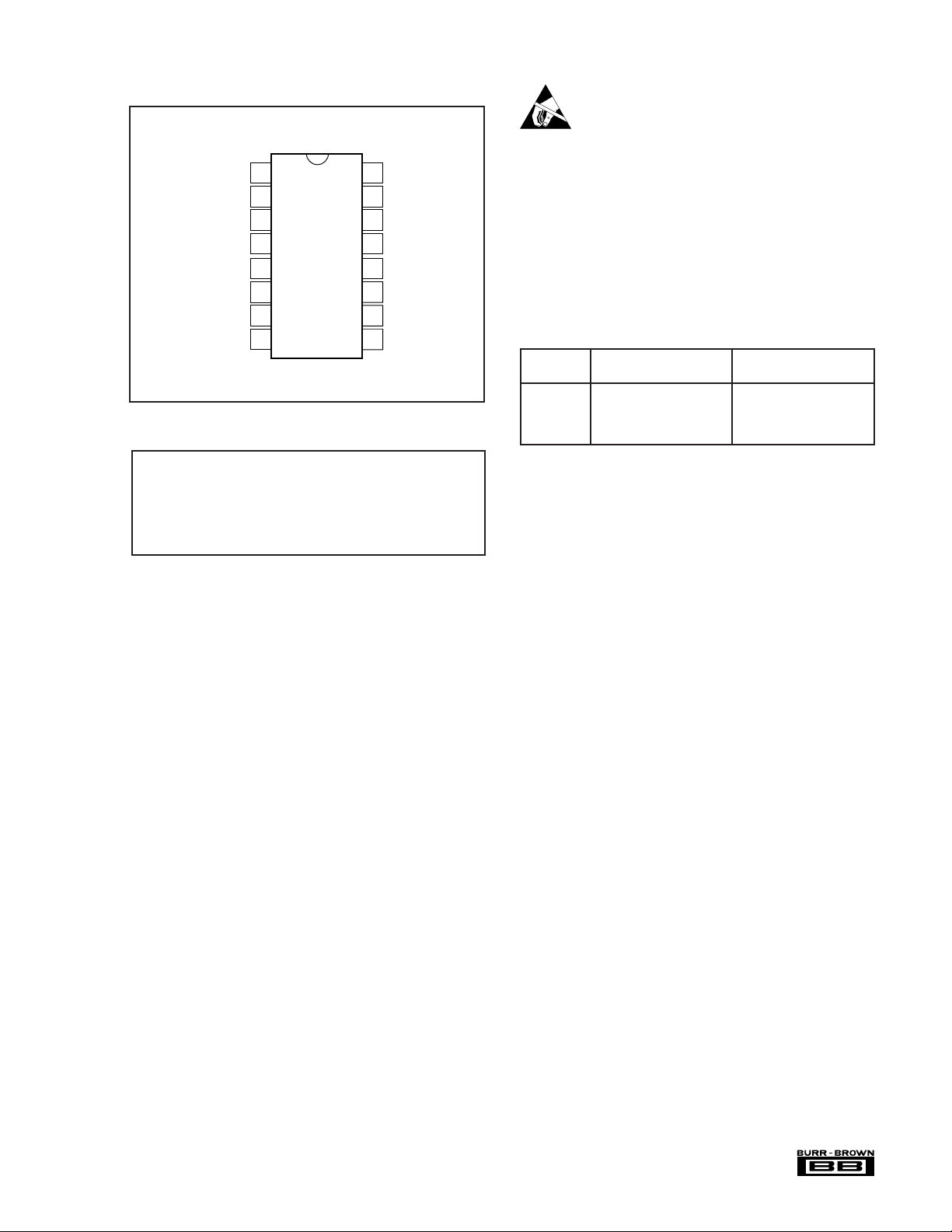
PIN CONFIGURATION
ELECTROSTATIC
Top View DIP
1
R
G
Guard –
Guard –
Guard +
Guard +
2
–
3
V
IN
4
5
+
6
V
IN
7
8
V–
NC: No Internal Connection.
16
R
G
15
NC
14
NC
13
V+
12
NC
11
V
O
10
NC
9
Ref
SOL-16
ABSOLUTE MAXIMUM RATINGS
Supply Voltage .................................................................................. ±18V
Input Voltage Range .......................................................................... ±40V
Output Short-Circuit (to ground) .............................................. Continuous
Operating Temperature ................................................. –40°C to +125°C
Storage Temperature ..................................................... –40°C to +125°C
Junction Temperature.................................................................... +150°C
Lead Temperature (soldering, 10s)............................................... +300°C
DISCHARGE SENSITIVITY
This integrated circuit can be damaged by ESD. Burr-Brown
recommends that all integrated circuits be handled with
appropriate precautions. Failure to observe proper handling
and installation procedures can cause damage.
ESD damage can range from subtle performance degradation
to complete device failure. Precision integrated circuits may
be more susceptible to damage because very small parametric
changes could cause the device not to meet its published
specifications.
PACKAGE INFORMATION
PRODUCT PACKAGE NUMBER
PACKAGE DRAWING
INA116PA 16-Pin Plastic DIP 180
INA116P 16-Pin Plastic DIP 180
INA116UA SOL-16 Surface-Mount 211
INA116U SOL-16 Surface-Mount 211
NOTE: (1) For detailed drawing and dimension table, please see end of data
sheet, or Appendix C of Burr-Brown IC Data Book.
(1)
The information provided herein is believed to be reliable; however, BURR-BROWN assumes no responsibility for inaccuracies or omissions. BURR-BROWN assumes
no responsibility for the use of this information, and all use of such information shall be entirely at the user’s own risk. Prices and specifications are subject to change
without notice. No patent rights or licenses to any of the circuits described herein are implied or granted to any third party. BURR-BROWN does not authorize or warrant
any BURR-BROWN product for use in life support devices and/or systems.
3
INA116
®
 Loading...