

Page 1

INA116
INA116
®
Ultra Low Input Bias Current
INSTRUMENTATION AMPLIFIER
INA1 16
FEATURES
● LOW INPUT BIAS CURRENT: 3fA typ
● BUFFERED GUARD DRIVE PINS
● LOW OFFSET VOLTAGE: 2mV max
● HIGH COMMON-MODE REJECTION:
84dB (G = 10)
● LOW QUIESCENT CURRENT: 1mA
● INPUT OVER-VOLTAGE PROTECTION:
APPLICATIONS
● LABORATORY INSTRUMENTATION
● pH MEASUREMENT
● ION–SPECIFIC PROBES
● LEAKAGE CURRENT MEASUREMENT
Guard
Guard
2
–
3
V
IN
Over-Voltage
4
1
Protection
+1
±40V
DESCRIPTION
The INA116 is a complete monolithic FET-input instrumentation amplifier with extremely low input bias
current.
yield input bias currents of 3fA at 25°C, and only 25fA
at 85°C. Its 3-op amp topology allows gains to be set
from 1 to 1000 by connecting a single external resistor.
Guard pins adjacent to both input connections can be
used to drive circuit board and input cable guards to
maintain extremely low input bias current.
The INA116 is available in 16-pin plastic DIP and SOL-16
surface-mount packages, specified for the –40°C to +85°C
temperature range.
V+
A
1
25kΩ
®
Difet
inputs and special guarding techniques
13
INA116
50kΩ
60kΩ60kΩ
G = 1 +
R
G
SBOS034
R
G
16
Guard
Guard
®
Difet
; Burr-Brown Corporation
International Airport Industrial Park • Mailing Address: PO Box 11400, Tucson, AZ 85734 • Street Address: 6730 S. Tucson Blvd., Tucson, AZ 85706 • Tel: (520) 746-1111 • Twx: 910-952-1111
Internet: http://www.burr-brown.com/ • FAXLine: (800) 548-6133 (US/Canada Only) • Cable: BBRCORP • Telex: 066-6491 • FAX: (520) 889-1510 • Immediate Product Info: (800) 548-6132
5
+
6
V
IN
Over-Voltage
7
Protection
+1
25kΩ
A
2
8
V–
A
3
60kΩ60kΩ
V
O
11
Ref
9
©1994 Burr-Brown Corporation PDS-1242B Printed in U.S.A. May, 1995
Page 2
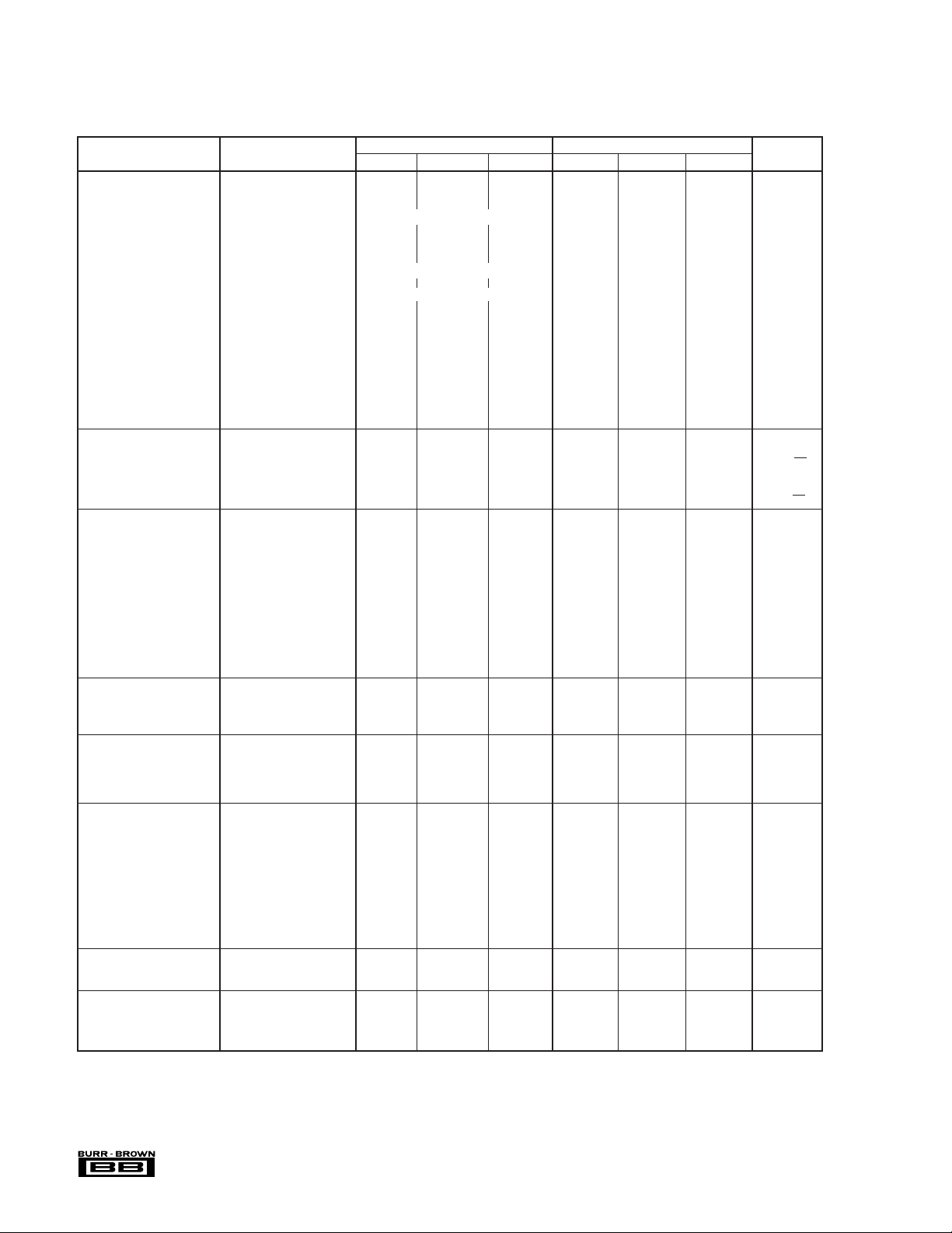
SPECIFICATIONS
AT TA = +25°C, VS = ±15V, RL = 10kΩ, unless otherwise noted.
INA116P, U INA116PA, UA
PARAMETER CONDITIONS MIN TYP MAX MIN TYP MAX UNITS
INPUT
Offset Voltage, RTI
Initial T
vs Temperature T
vs Power Supply V
Long-Term Stability ±1 ±5/G ✻ µV/mo
Bias Current ±3 ±25 ✻ ±100 fA
vs Temperature See Typical Curve ✻
Offset Current ±1 ±25 ✻ ±100 fA
vs Temperature See Typical Curve ✻
Impedance, Differential >10
Common-Mode >10
Common-Mode Voltage Range
Safe Input Voltage ±40 ✻ V
Common-Mode Rejection V
NOISE
Voltage Noise, RTI G = 1000, R
f = 1kHz 28 ✻ nV/√Hz
f
= 0.1Hz to 10Hz 2 ✻ µVp-p
B
Current Noise
f = 1kHz 0.1 ✻ fA/√Hz
GAIN
Gain Equation 1+(50kΩ/R
Range of Gain 1 1000 ✻✻V/V
Gain Error G = 1 ±0.01 ±0.05 ✻ 0.1 %
Gain vs Temperature
50kΩ Resistance
(1)
(1)(2)
Nonlinearity G = 1 ±0.0005 ±0.005 ✻ ±0.01 % of FSR
GUARD OUTPUTS
Offset Voltage ±15 ±50 ✻✻mV
Output Impedance 650 ✻ Ω
Current Drive +2/–0.05 ✻ mA
OUTPUT
Voltage Positive R
Negative R
Load Capacitance Stability 1000 ✻ pF
Short-Circuit Current +5/–12 ✻ mA
FREQUENCY RESPONSE
Bandwidth, –3dB G = 1 800 ✻ kHz
Slew Rate G = 10 to 200 0.8 ✻ V/µs
Settling Time, 0.01% 10V Step, G = 1 22 ✻ µs
Output Overload Recovery 50% Overdrive 20 ✻ µs
POWER SUPPLY
Voltage Range ±4.5 ±15 ±18 ✻✻✻V
Current V
TEMPERATURE RANGE
Specification –40 85 ✻✻°C
Operating –40 125 ✻✻°C
θ
JA
✻ Specification same as INA116P
NOTE: (1) Guaranteed by wafer test. (2) Temperature coefficient of the “50kΩ” term in the gain equation.
= +25°C ±0.5 ±0.5/G ±2 ±2/G ✻ ±5 ±5/G mV
A
= T
to T
A
MIN
= ±4.5V to ±18V ±10 ±15/G ±50 ±100/G ✻ ±100 ±200/G µV/V
S
= ±11V, ∆RS = 1kΩ
CM
V
= ±5V, G = 1000 86 94 80 ✻ dB
CM
MAX
G = 1 80 89 73 ✻ dB
G = 10 84 92 78 ✻ dB
G = 100 86 94 80 ✻ dB
= 0Ω
S
See Typical Curve ✻
15
/0.2 ✻ Ω/pF
15
(V+)–4 (V+)–2 ✻✻ V
(V–)+4 (V–)+2.4 ✻✻ V
/7 ✻ Ω/pF
) ✻ V/V
G
G = 10 ±0.25 ±0.4 ✻ ±0.5 %
G = 100 ±0.35 ±0.5 ✻ ±0.7 %
G = 1000 ±1.25 ✻ %
G = 1 ±5 ±10 ✻ ±20 ppm/°C
G = 10 ±0.001 ±0.005 ✻ ±0.01 % of FSR
G = 100 ±0.001 ±0.005 ✻ ±0.01 % of FSR
±25 ±100 ✻ ±100 ppm/°C
G = 1000 ±0.005 ✻ % of FSR
= 10kΩ (V+) –1 (V+) –0.7 ✻✻ V
L
= 10kΩ (V–) +0.35 (V–) +0.2 ✻✻ V
L
G = 10 500 ✻ kHz
G = 100 70 ✻ kHz
G = 1000 7 ✻ kHz
G = 10 25 ✻ µs
G = 100 145 ✻ µs
G = 1000 400 ✻ µs
= 0V ±1 ±1.4 ✻✻mA
IN
80 ✻ ° C/W
®
INA116
2
Page 3
PIN CONFIGURATION
ELECTROSTATIC
Top View DIP
1
R
G
Guard –
Guard –
Guard +
Guard +
2
–
3
V
IN
4
5
+
6
V
IN
7
8
V–
NC: No Internal Connection.
16
R
G
15
NC
14
NC
13
V+
12
NC
11
V
O
10
NC
9
Ref
SOL-16
ABSOLUTE MAXIMUM RATINGS
Supply Voltage .................................................................................. ±18V
Input Voltage Range .......................................................................... ±40V
Output Short-Circuit (to ground) .............................................. Continuous
Operating Temperature ................................................. –40°C to +125°C
Storage Temperature ..................................................... –40°C to +125°C
Junction Temperature.................................................................... +150°C
Lead Temperature (soldering, 10s)............................................... +300°C
DISCHARGE SENSITIVITY
This integrated circuit can be damaged by ESD. Burr-Brown
recommends that all integrated circuits be handled with
appropriate precautions. Failure to observe proper handling
and installation procedures can cause damage.
ESD damage can range from subtle performance degradation
to complete device failure. Precision integrated circuits may
be more susceptible to damage because very small parametric
changes could cause the device not to meet its published
specifications.
PACKAGE INFORMATION
PRODUCT PACKAGE NUMBER
PACKAGE DRAWING
INA116PA 16-Pin Plastic DIP 180
INA116P 16-Pin Plastic DIP 180
INA116UA SOL-16 Surface-Mount 211
INA116U SOL-16 Surface-Mount 211
NOTE: (1) For detailed drawing and dimension table, please see end of data
sheet, or Appendix C of Burr-Brown IC Data Book.
(1)
The information provided herein is believed to be reliable; however, BURR-BROWN assumes no responsibility for inaccuracies or omissions. BURR-BROWN assumes
no responsibility for the use of this information, and all use of such information shall be entirely at the user’s own risk. Prices and specifications are subject to change
without notice. No patent rights or licenses to any of the circuits described herein are implied or granted to any third party. BURR-BROWN does not authorize or warrant
any BURR-BROWN product for use in life support devices and/or systems.
3
INA116
®
Page 4
TYPICAL PERFORMANCE CURVES
At TA = +25°C, VS = ±15V, RL = 10kΩ, unless otherwise noted.
60
G = 1000
50
40
G = 100
30
20
G = 10
Gain (dB)
10
0
G = 1
–10
–20
1k 10k 100k 1M 10M
120
100
80
60
40
Power Supply Rejection (dB)
20
GAIN vs FREQUENCY
Frequency (Hz)
POSITIVE POWER SUPPLY REJECTION
vs FREQUENCY
G = 10V/V
G = 1V/V
G = 1000V/V
G = 100V/V
100
Common-Mode Rejection (dB)
120
100
Power Supply Rejection (dB)
COMMON-MODE REJECTION vs FREQUENCY
90
80
70
60
50
40
30
20
10
0
10 100 1k 10k 100k
Frequency (Hz)
NEGATIVE POWER SUPPLY REJECTION
vs FREQUENCY
80
60
40
20
G = 1000V/V
G = 100V/V
G = 10V/V
G = 1V/V
G = 10 < 100
G = 1
G = 1k
0
1 10 100 1k 10k 100k
Frequency (Hz)
15
10
–5
Input Bias Current (fA)
–10
–15
INPUT BIAS CURRENT vs INPUT VOLTAGE
5
0
–15 –10 –5 0 5 10 15
Input Voltage (V)
®
INA116
0
1 10 100 1k 10k 100k
1000
100
10
Input Bias Current (fA)
1
–75 –50 –25 0 25 50 75 100 125
4
Frequency (Hz)
INPUT BIAS CURRENT vs TEMPERATURE
I
B
Measurement Limit
I
OS
Page 5

TYPICAL PERFORMANCE CURVES (CONT)
At TA = +25°C, VS = ±15V, RL = 10kΩ, unless otherwise noted.
INPUT COMMON-MODE RANGE
15
G ≥ 10
vs OUTPUT VOLTAGE
10
G = 1G = 1
5
V
0
V
–5
Common-Mode Voltage (V)
–10
D/2
D/2
V
CM
–
+
–
+
G = 1
–15V
+15V
INA116
Ref
V
O
–15
–15 –10 0 5 15–5
10
Output Voltage (V)
INPUT OVER-VOLTAGE V/I CHARACTERISTICS
4
3
2
G = 1V/V
G = 1000V/V
1
0
–1
Input Current (mA)
–2
G = 1000V/V
G = 1V/V
–3
–4
–40 –30 –20 –10 0 10 20 30 40
Input Voltage (V)
G ≥ 10
G = 1
10k
INPUT REFERRED NOISE vs FREQUENCY
1k
G = 1V/V
100
G = 1000V/V
Voltage Noise Density (nV/√ Hz)
10
G = 10V/V
Bandwidth Limit
110 1k100
Frequency (Hz)
OFFSET VOLTAGE WARM-UP
15
10
G ≥ 10
G = 1
5
0
–5
Offset Voltage Change (µV)
–10
G = 1
G ≥ 10
–15
0 5 10 15 20 25
Time After Power Supply Turn-On (s)
10k
INPUT OFFSET VOLTAGE DRIFT
PRODUCTION DISTRIBUTION
G = 100
0.5
G = 10
2
G = 1
Production Distribution (%)
0.5
9
3
2
–80 –60 –40 –20
Offset Voltage Drift (µV/°C)
40
26
19
7
38
24
9
17
15
12
0.5
6
20
5
1
1
18
14
44
0 20406080
0.5
1.6
1.4
1.2
1.0
0.8
Quiescent Current (µA)
0.6
0.4
–75 –50 –25
5
QUIESCENT CURRENT AND SLEW RATE
vs TEMPERATURE
I
Q
SR
0 25 50 75 100 125
Temperature (°C)
INA116
1.4
1.2
1.0
0.8
Slew Rate (V/µs)
0.6
0.4
®
Page 6

TYPICAL PERFORMANCE CURVES (CONT)
At TA = +25°C, VS = ±15V, RL = 10kΩ, unless otherwise noted.
MAXIMUM OUTPUT VOLTAGE vs FREQUENCY
32
G = 10, 100
28
G = 1
24
20
16
12
8
Peak-to-Peak Output Voltage (V)
4
0
100 1k 10k 100k 1M
SMALL SIGNAL RESPONSE SMALL SIGNAL RESPONSE
G = 1000
Frequency (Hz)
500nV/div
VOLTAGE NOISE, 0.1 TO 10Hz
INPUT-REFERRED, G ≥ 100
1s/div
G=1
G=10
G=1
G=10
G=100
20mV/div
G=1000
10µs/div
LARGE SIGNAL RESPONSE LARGE SIGNAL RESPONSE
G=100
5V/div
G=1000
100µs/div
20mV/div
5V/div
®
INA116
100µs/div
100µs/div
6
Page 7

APPLICATIONS INFORMATION
Figure 1 shows the connections required for basic operation
of the INA116. Applications with noisy or high impedance
power supplies may require decoupling capacitors close to
the supply pins as shown.
The output is referred to the output reference (Ref) terminal
which is normally grounded. This must be a low impedance
connection to assure good common-mode rejection. A resistance of 30Ω in series with this connection will cause a
typical device to degrade to approximately 72dB CMR at
G = 1.
The 50kΩ term in equation 1 is the sum of the two feedback
resistors of A
and A2. These on-chip metal film resistors are
1
laser trimmed to accurate absolute values. The accuracy and
temperature coefficient of these resistors are included in the
gain accuracy and drift specifications of the INA116.
The stability and temperature drift of R
’s contribution to gain accuracy and drift can be directly
R
G
also affect gain.
G
inferred from the gain equation (1). Low resistor values
required for high gain make wiring resistance important.
Sockets add to the wiring resistance that will contribute
additional gain error in gains of approximately 100 or
greater.
SETTING THE GAIN
Gain of the INA116 is set by connecting a single external
resistor, R
, as shown. The gain is—
G
G =1 +
50 kΩ
R
G
(1)
Commonly used gains and resistor values are shown in
Figure 1.
4
3
Input Guards
See Text.
–
V
IN
+
V
IN
R
2
1
G
16
5
6
7
Over-Voltage
Protection
Over-Voltage
Protection
+1
+1
OFFSET TRIMMING
The INA116 is laser trimmed for low offset voltage and
offset voltage drift; most applications require no external
offset adjustment. Figure 2 shows an optional circuit for
trimming the output offset voltage. A voltage applied to the
Ref terminal is summed at the output. Op amp A
a low source impedance for the Ref terminal, assuring good
common-mode rejection.
V+
0.1µF
13
INA116
A
1
R
FB
25kΩ
R
FB
25kΩ
A
2
R
60kΩ
R
60kΩ
1
3
R
60kΩ
A
3
60kΩ
2
R
4
G = 1 +
11
Ref
9
50kΩ
R
V
G
O
provides
1
DESIRED
GAIN
1
2
5
10
20
50
100
200
500
1000
2000
5000
10000
NC: No Connection.
FIGURE 1. Basic Connections.
R
G
(Ω)
NC
50.00k
12.50k
5.556k
2.632k
1.02k
505.1
251.3
100.2
50.05
25.01
10.00
5.001
NEAREST 1% R
(Ω)
NC
49.9k
12.4k
5.62k
2.61k
1.02k
511
249
100
49.9
24.9
10
4.99
8
0.1µF
G
7
V–
Also drawn in simplified form:
–
V
IN
INA116
R
G
+
V
IN
INA116
Ref
V
O
®
Page 8

–
V
IN
INA116
R
G
+
V
IN
±10mV
Adjustment Range
NOTE: (1) For wider trim range required
in high gains, scale resistor values larger
Ref
V
O
OPA131
10kΩ
V+
(1)
V–
100µA
1/2 REF200
(1)
100Ω
(1)
100Ω
100µA
1/2 REF200
FIGURE 2. Optional Trimming of Output Offset Voltage.
INPUT BIAS CURRENT RETURN PATH
Input circuitry must provide an input bias current path for
proper operation. Figure 3 shows resistors R
and R2 to
1
provide an input current path. Without these resistors, the
inputs would eventually float to a potential that exceeds the
common-mode range of the INA116 and the input amplifiers
would saturate. Because of its exceedingly low input bias
current, improperly biased inputs may operate normally for
a period of time after power is first applied, or operate
intermittently.
Crystal or
Transducer
Capacitive
Sensor
100MΩ
Ceramic
Polarizing
Voltage
100MΩ
100MΩ
100MΩ
R
1
R
1
100MΩ
R
2
100MΩ
R
2
INA116
INA116
V
O
V
O
CIRCUIT BOARD LAYOUT AND ASSEMBLY
Careful circuit board layout and assembly techniques are
required to achieve the exceptionally low input bias current
performance of the INA116. Guard terminals adjacent to
both inputs make it easy to properly guard the critical input
terminal layout. Since traces are not required to run between
device pins, this layout is easily accomplished, even with the
surface mount package. The guards should completely encircle their respective input connections—see Figure 4. Both
sides of the circuit board should be guarded, even if only one
side has an input terminal conductor. Route any timevarying signals away from the input terminals. Solder mask
should not cover the input and guard traces since this can
increase leakage.
Guard Top and
Bottom of Circuit Board.
FIGURE 4. Circuit Board Guard Layout.
After assembly, the circuit board should be cleaned. Commercial solvents should be chosen according to the soldering
method and flux used. Solvents should be cleaned and
replaced often. Solvent cleaning should be followed by a deionized water rinse and 85°C bake out.
Sockets can be used, but select and evaluate them carefully
for best results. Use caution when installing the INA116 in
a socket. Careless handling can contaminate the plastic near
the input pins, dramatically increasing leakage current.
A proven low leakage current assembly method is to bend
the input pins outward so they do not contact the circuit
board. Input connections are made in air and soldered
directly to the input pin. This technique is often not practical
or production-worthy. It is, however, a useful technique for
evaluation and testing and provides a benchmark with which
to compare other wiring techniques. The circuit board guarding techniques discussed normally reduce leakage to acceptable levels.
A solid mechanical assembly is required for good results.
Nearby plastic parts can be especially troublesome since a
static charge can develop and the slightest motion or vibration will couple charge to the inputs. Place a Faraday shield
around the whole amplifier and input connection assembly
to eliminate stray fields.
FIGURE 3. Providing An Input Bias Current Path.
®
INA116
8
Page 9

INPUT CONNECTIONS
INA116
6
3
1
16
5.62kΩ
13
8
9
11
V
O
G = 10
+15
–15
Solution
Ground
Sample
Electrode
Reference
Electrode
Some applications must make high impedance input connections to external sensors or input connectors. To assure low
leakage, the input should be guarded all the way to the signal
source—see Figure 5. Coaxial cable can be used with the
shield driven by the guard. A separate connection is required
to provide a ground reference at the signal source. Triaxial
cable may reduce noise pickup and provides the ground
reference at the source. Drive the inner shield at guard
High-Z
Source
Two coaxial cables and ground
V
1MΩ
High-Z
Source
Two triaxial cables
V
potential and ground the outer shield. Two separate guarded
lines are required if both the inverting and non-inverting
inputs are brought to the source.
The guard drive output current is limited to approximately
+2mA/–50µA. For slow input signals the internal guard
output can directly drive a cable shield. With fast input
signals, however, the guard may not provide sufficient
output current to rapidly charge the cable capacitance. An op
amp buffer may be required as shown in Figure 6.
–
V
IN
+
V
IN
–
V
IN
+
V
IN
1MΩ
FIGURE 5. Input Cable Guarding Circuits.
Circuit Board
Guard
V
IN
Op amp buffer helps
guard cables with
fast input signals—
see text.
FIGURE 6. Buffered Guard Drive.
Cable
150Ω
OPA131
FIGURE 7. pH or Ion Measurement System.
9
INA116
®
Page 10

PACKAGE OPTION ADDENDUM
www.ti.com
2-Oct-2006
PACKAGING INFORMATION
Orderable Device Status
(1)
Package
Type
Package
Drawing
Pins Package
Qty
Eco Plan
INA116PA ACTIVE PDIP N 16 25 Green (RoHS &
no Sb/Br)
INA116PAG4 ACTIVE PDIP N 16 25 Green (RoHS &
no Sb/Br)
INA116UA ACTIVE SOIC DW 16 48 Green (RoHS &
no Sb/Br)
INA116UAG4 ACTIVE SOIC DW 16 48 Green (RoHS &
no Sb/Br)
(1)
The marketing status values are defined as follows:
ACTIVE: Product device recommended for new designs.
LIFEBUY: TI has announced that the device will be discontinued, and a lifetime-buy period is in effect.
NRND: Not recommended for new designs. Device is in production to support existing customers, but TI does not recommend using this part in
a new design.
PREVIEW: Device has been announced but is not in production. Samples may or may not be available.
OBSOLETE: TI has discontinued the production of the device.
(2)
Eco Plan - The planned eco-friendly classification: Pb-Free (RoHS), Pb-Free (RoHS Exempt), or Green (RoHS & no Sb/Br) - please check
http://www.ti.com/productcontent for the latest availability information and additional product content details.
TBD: The Pb-Free/Green conversion plan has not been defined.
Pb-Free (RoHS): TI's terms "Lead-Free" or "Pb-Free" mean semiconductor products that are compatible with the current RoHS requirements
for all 6 substances, including the requirement that lead not exceed 0.1% by weight in homogeneous materials. Where designed to be soldered
at high temperatures, TI Pb-Free products are suitable for use in specified lead-free processes.
Pb-Free (RoHS Exempt): This component has a RoHS exemption for either 1) lead-based flip-chip solder bumps used between the die and
package, or 2) lead-based die adhesive used between the die and leadframe. The component is otherwise considered Pb-Free (RoHS
compatible) as defined above.
Green (RoHS & no Sb/Br): TI defines "Green" to mean Pb-Free (RoHS compatible), and free of Bromine (Br) and Antimony (Sb) based flame
retardants (Br or Sb do not exceed 0.1% by weight in homogeneous material)
(2)
Lead/Ball Finish MSL Peak Temp
CU NIPDAU N / A for Pkg Type
CU NIPDAU N / A for Pkg Type
CU NIPDAU Level-3-260C-168 HR
CU NIPDAU Level-3-260C-168 HR
(3)
(3)
MSL, Peak Temp. -- The Moisture Sensitivity Level rating according to the JEDEC industry standard classifications, and peak solder
temperature.
Important Information and Disclaimer:The information provided on this page represents TI's knowledge and belief as of the date that it is
provided. TI bases its knowledge and belief on information provided by third parties, and makes no representation or warranty as to the
accuracy of such information. Efforts are underway to better integrate information from third parties. TI has taken and continues to take
reasonable steps to provide representative and accurate information but may not have conducted destructive testing or chemical analysis on
incoming materials and chemicals. TI and TI suppliers consider certain information to be proprietary, and thus CAS numbers and other limited
information may not be available for release.
In no event shall TI's liability arising out of such information exceed the total purchase price of the TI part(s) at issue in this document sold by TI
to Customer on an annual basis.
Addendum-Page 1
Page 11

IMPORTANT NOTICE
Texas Instruments Incorporated and its subsidiaries (TI) reserve the right to make corrections, modifications,
enhancements, improvements, and other changes to its products and services at any time and to discontinue
any product or service without notice. Customers should obtain the latest relevant information before placing
orders and should verify that such information is current and complete. All products are sold subject to TI’s terms
and conditions of sale supplied at the time of order acknowledgment.
TI warrants performance of its hardware products to the specifications applicable at the time of sale in
accordance with TI’s standard warranty. T esting and other quality control techniques are used to the extent TI
deems necessary to support this warranty . Except where mandated by government requirements, testing of all
parameters of each product is not necessarily performed.
TI assumes no liability for applications assistance or customer product design. Customers are responsible for
their products and applications using TI components. To minimize the risks associated with customer products
and applications, customers should provide adequate design and operating safeguards.
TI does not warrant or represent that any license, either express or implied, is granted under any TI patent right,
copyright, mask work right, or other TI intellectual property right relating to any combination, machine, or process
in which TI products or services are used. Information published by TI regarding third-party products or services
does not constitute a license from TI to use such products or services or a warranty or endorsement thereof.
Use of such information may require a license from a third party under the patents or other intellectual property
of the third party, or a license from TI under the patents or other intellectual property of TI.
Reproduction of information in TI data books or data sheets is permissible only if reproduction is without
alteration and is accompanied by all associated warranties, conditions, limitations, and notices. Reproduction
of this information with alteration is an unfair and deceptive business practice. TI is not responsible or liable for
such altered documentation.
Resale of TI products or services with statements different from or beyond the parameters stated by TI for that
product or service voids all express and any implied warranties for the associated TI product or service and
is an unfair and deceptive business practice. TI is not responsible or liable for any such statements.
Following are URLs where you can obtain information on other Texas Instruments products and application
solutions:
Products Applications
Amplifiers amplifier.ti.com Audio www.ti.com/audio
Data Converters dataconverter.ti.com Automotive www.ti.com/automotive
DSP dsp.ti.com Broadband www.ti.com/broadband
Interface interface.ti.com Digital Control www.ti.com/digitalcontrol
Logic logic.ti.com Military www.ti.com/military
Power Mgmt power.ti.com Optical Networking www.ti.com/opticalnetwork
Microcontrollers microcontroller.ti.com Security www.ti.com/security
Low Power Wireless www.ti.com/lpw Telephony www.ti.com/telephony
Video & Imaging www.ti.com/video
Wireless www.ti.com/wireless
Mailing Address: Texas Instruments
Post Office Box 655303 Dallas, Texas 75265
Copyright 2006, Texas Instruments Incorporated
 Loading...