

Burr Brown INA115BU, INA115AU-1K, INA115AU Datasheet
©1992 Burr-Brown Corporation PDS-1169B Printed in U.S.A. October, 1993
INA115
Precision
INSTRUMENTATION AMPLIFIER
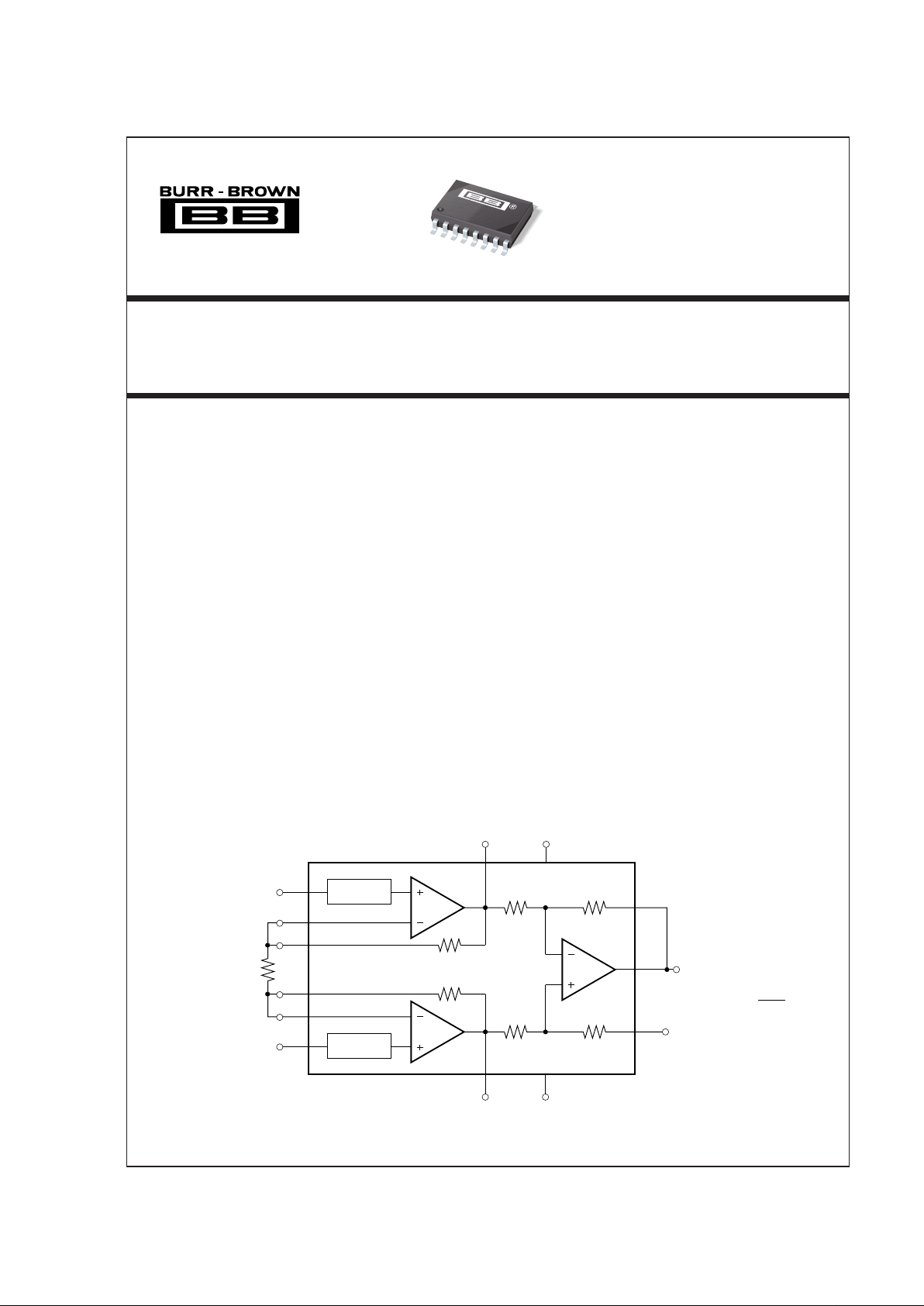
A
1
A
2
A
3
12
11
10
25kΩ25kΩ
25kΩ25kΩ
13
7
5
4
V
IN
V
IN
R
G
V+
V–
INA115
Ref
V
O
G = 1 +
50kΩ
R
G
–
+
Over-Voltage
Protection
25kΩ
25kΩ
Over-Voltage
Protection
Feedback
15
14
3
2
8
V
O2
V
O1
1
FEATURES
● LOW OFFSET VOLTAGE: 50µV max
● LOW DRIFT: 0.25µV/
°C max
● LOW INPUT BIAS CURRENT: 2nA max
● HIGH COMMON-MODE REJECTION:
115dB min
● INPUT OVER-VOLTAGE PROTECTION:
±40V
● WIDE SUPPLY RANGE:
±2.25 TO ±18V
● LOW QUIESCENT CURRENT: 3mA max
● SOL-16 SURFACE-MOUNT PACKAGE
APPLICATIONS
● SWITCHED-GAIN AMPLIFIER
● BRIDGE AMPLIFIER
● THERMOCOUPLE AMPLIFIER
● RTD SENSOR AMPLIFIER
● MEDICAL INSTRUMENTATION
● DATA ACQUISITION
DESCRIPTION
The INA115 is a low cost, general purpose instrumentation amplifier offering excellent accuracy. Its versatile three-op amp design and small size make it ideal
for a wide range of applications. Similar to the model
INA114, the INA115 provides additional connections
to the input op amps, A
1
and A2, which improve gain
accuracy in high gains and are useful in forming
switched-gain amplifiers.
A single external resistor sets any gain from 1 to
10,000. Internal input protection can withstand up to
±40V without damage.
The INA115 is laser trimmed for very low offset
voltage (50µV), drift (0.25µV/˚C) and high commonmode rejection (115dB at G=1000). It operates with
power supplies as low as ±2.25V, allowing use in
battery operated and single 5V supply systems. Quiescent current is 3mA maximum.
The INA115 is available in the SOL-16 surface-mount
package, specified for the –40°C to +85°C temperature range.
®
INA115
International Airport Industrial Park • Mailing Address: PO Box 11400, Tucson, AZ 85734 • Street Address: 6730 S. Tucson Blvd., Tucson, AZ 85706 • Tel: (520) 746-1111 • Twx: 910-952-1111
Internet: http://www.burr-brown.com/ • FAXLine: (800) 548-6133 (US/Canada Only) • Cable: BBRCORP • Telex: 066-6491 • FAX: (520) 889-1510 • Immediate Product Info: (800) 548-6132
2
®
INA115
SPECIFICATIONS
ELECTRICAL
At TA = +25°C, VS = ±15V, RL = 2kΩ unless otherwise noted.
✻ Specification same as INA115BU.
NOTE: (1) Temperature coefficient of the “50kΩ” term in the gain equation. (2) Output specifications are for output amplifier, A
3
. A1 and A2 provide the same output
voltage swing but have less output current drive. A
1
and A2 can drive external loads of 25kΩ || 200pF.
INA115BU INA115AU
PARAMETER CONDITIONS MIN TYP MAX MIN TYP MAX UNITS
INPUT
Offset Voltage, RTI
Initial T
A
= +25°C ±10 + 20/G ±50 + 100/G ±25 + 30/G ±125 + 500/G µV
vs Temperature T
A
= T
MIN
to T
MAX
±0.1 + 0.5/G ±0.25 + 5/G ±0.25 + 5/G ±1 + 10/G µV/°C
vs Power Supply V
S
= ±2.25V to ±18V 0.5 + 2/G 3 + 10/G ✻✻µV/V
Long-Term Stability ±0.2 + 0.5/G ✻ µV/mo
Impedance, Differential 10
10
|| 6 ✻ Ω || pF
Common-Mode 10
10
|| 6 ✻ Ω || pF
Input Common-Mode Range ±11 ±13.5 ✻✻ V
Safe Input Voltage ±40 ✻ V
Common-Mode Rejection V
CM
= ±10V, ∆RS = 1kΩ
G = 1 80 96 75 90 dB
G = 10 96 115 90 106 dB
G = 100 110 120 106 110 dB
G = 1000 115 120 106 110 dB
BIAS CURRENT ±0.5 ±2 ✻ ±5nA
vs Temperature ±8 ✻ pA/°C
OFFSET CURRENT ±0.5 ±2 ✻ ±5nA
vs Temperature ±8 ✻ pA/°C
NOISE VOLTAGE, RTI G = 1000, R
S
= 0Ω
f = 10Hz 15 ✻ nV/√Hz
f = 100Hz 11 ✻ nV/√Hz
f = 1kHz 11 ✻ nV/√Hz
f
B
= 0.1Hz to 10Hz 0.4 ✻ µVp-p
Noise Current
f=10Hz 0.4 ✻ pA/√Hz
f=1kHz 0.2 ✻ pA/√Hz
f
B
= 0.1Hz to 10Hz 18 ✻ pAp-p
GAIN
Gain Equation 1 + (50kΩ/R
G
) ✻ V/V
Range of Gain 1 10000 ✻✻V/V
Gain Error G = 1 ±0.01 ±0.05 ✻✻%
G = 10 ±0.02 ±0.4 ✻ ±0.5 %
G = 100 ±0.05 ±0.5 ✻ ±0.7 %
G = 1000 ±0.5 ±1 ✻ ±2%
Gain vs Temperature G = 1 ±2 ±10 ✻ ±10 ppm/°C
50kΩ Resistance
(1)
±25 ±100 ✻✻ppm/°C
Nonlinearity G = 1 ±0.0001 ±0.001 ✻ ±0.002 % of FSR
G = 10 ±0.0005 ±0.002 ✻ ±0.004 % of FSR
G = 100 ±0.0005 ±0.002 ✻ ±0.004 % of FSR
G = 1000 ±0.002 ±0.01 ✻ ±0.02 % of FSR
OUTPUT
(2)
Voltage IO = 5mA, T
MIN
to T
MAX
±13.5 ±13.7 ✻✻ V
V
S
= ±11.4V, RL = 2kΩ±10 ±10.5 ✻✻ V
V
S
= ±2.25V, RL = 2kΩ±1 ±1.5 ✻✻ V
Load Capacitance Stability 1000 ✻ pF
Short Circuit Current +20/–15 ✻ mA
FREQUENCY RESPONSE
Bandwidth, –3dB G = 1 1 ✻ MHz
G = 10 100 ✻ kHz
G = 100 10 ✻ kHz
G = 1000 1 ✻ kHz
Slew Rate V
O
= ±10V, G = 10 0.3 0.6 ✻✻ V/µs
Settling Time, 0.01% G = 1 18 ✻ µs
G = 10 20 ✻ µs
G = 100 120 ✻ µs
G = 1000 1100 ✻ µs
Overload Recovery 50% Overdrive 20 ✻ µs
POWER SUPPLY
Voltage Range ±2.25 ±15 ±18 ✻✻ ✻V
Current V
IN
= 0V ±2.2 ±3 ✻✻mA
TEMPERATURE RANGE
Specification –40 +85 ✻✻°C
Operating –40 +125 ✻✻°C
θ
JA
80 ✻ °C/W
3
®
INA115
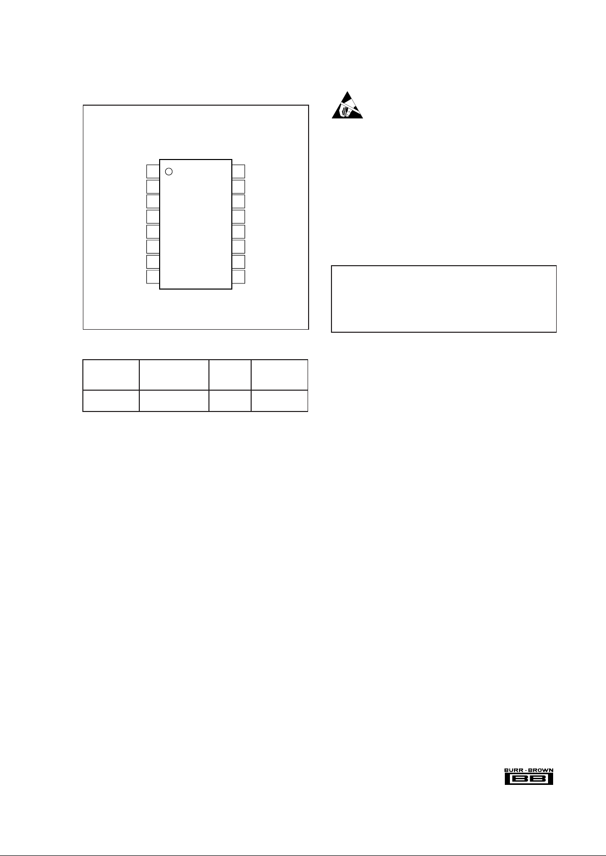
PIN CONFIGURATIONS
ELECTROSTATIC
DISCHARGE SENSITIVITY
This integrated circuit can be damaged by ESD. Burr-Brown
recommends that all integrated circuits be handled with appropriate precautions. Failure to observe proper handling and
installation procedures can cause damage.
ESD damage can range from subtle performance degradation
to complete device failure. Precision integrated circuits may
be more susceptible to damage because very small parametric
changes could cause the device not to meet its published
specifications.
V
O1
Gain Sense
1
R
G
V
–
IN
V
+
IN
NC
V–
V
O2
NC
Gain Sense
2
R
G
V+
Feedback
V
O
Ref
NC
1
2
3
4
5
6
7
8
16
15
14
13
12
11
10
9
U Package SOL-16 Surface-Mount
Top View
PACKAGE
DRAWING TEMPERATURE
PRODUCT PACKAGE NUMBER
(1)
RANGE
INA115AU SOL-16 Surface-Mount 211 –40°C to +85°C
INA115BU SOL-16 Surface-Mount 211 –40°C to +85°C
NOTE: (1) For detailed drawing and dimension table, please see end of data
sheet, or Appendix C of Burr-Brown IC Data Book.
PACKAGE/ORDERING INFORMATION
Supply Voltage .................................................................................. ±18V
Input Voltage Range .......................................................................... ±40V
Output Short-Circuit (to ground) .............................................. Continuous
Operating Temperature ................................................. –40°C to +125°C
Storage Temperature ..................................................... –40°C to +125°C
Junction Temperature .................................................................... +150°C
Lead Temperature (soldering, 10s)............................................... +300°C
ABSOLUTE MAXIMUM RATINGS
The information provided herein is believed to be reliable; however, BURR-BROWN assumes no responsibility for inaccuracies or omissions. BURR-BROWN assumes
no responsibility for the use of this information, and all use of such information shall be entirely at the user’s own risk. Prices and specifications are subject to change
without notice. No patent rights or licenses to any of the circuits described herein are implied or granted to any third party. BURR-BROWN does not authorize or warrant
any BURR-BROWN product for use in life support devices and/or systems.
4
®
INA115
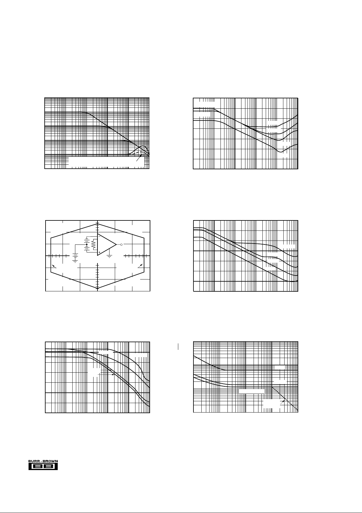
TYPICAL PERFORMANCE CURVES
At TA = +25°C, VS = ±15V, unless otherwise noted.
INPUT COMMON-MODE VOLTAGE RANGE
vs OUTPUT VOLTAGE
Output Voltage (V)
Common-Mode Voltage (V)
–15 –10 0 5 15–5
15
10
5
0
–5
–10
–15
10
Limited by A
1
+ Output Swing
A3 – Output
Swing Limit
A3 + Output
Swing Limit
Limited by A
2
– Output Swing
Limited by A
1
– Output Swing
Limited by A
2
+ Output Swing
V
D/2
–
+
–
+
V
CM
V
O
(Any Gain)
V
D/2
POSITIVE POWER SUPPLY REJECTION
vs FREQUENCY
Frequency (Hz)
Power Supply Rejection (dB)
10 100 10k 1M1k
140
120
100
80
60
40
20
0
100k
G = 1
G = 10
G = 100
G = 1000
NEGATIVE POWER SUPPLY REJECTION
vs FREQUENCY
Frequency (Hz)
Power Supply Rejection (dB)
10 100 10k 1M1k
140
120
100
80
60
40
20
0
100k
G = 1
G = 10
G = 100
G = 1000
INPUT- REFERRED NOISE VOLTAGE
vs FREQUENCY
Frequency (Hz)
Input-Referred Noise Voltage (nV/√ Hz)
110 1k100
1k
100
10
1
10k
G = 1
G = 10
G = 100, 1000
G = 1000
BW Limit
GAIN vs FREQUENCY
Frequency (Hz)
Gain (V/V)
10 100 10k 100k 1M1k
1k
100
10
1
VO1 connected to Gain Sense1 and
V
O2
connected to Gain Sense2 . See text.
COMMON-MODE REJECTION vs FREQUENCY
Frequency (Hz)
Common-Mode Rejection (dB)
10 100 10k 100k 1M1k
140
120
100
80
60
40
20
0
G = 1k
G = 100
G = 10
G = 1
G = 100, 1k
G = 10
 Loading...