

Burr Brown INA110KU, INA110KP, INA110AG, INA110SG, INA110KU-1K Datasheet
INA110
Fast-Settling FET-Input
INSTRUMENTATION AMPLIFIER
APPLICATIONS
● MULTIPLEXED INPUT DATA
ACQUISITION SYSTEM
● FAST DIFFERENTIAL PULSE AMPLIFIER
● HIGH SPEED GAIN BLOCK
● AMPLIFICATION OF HIGH IMPEDANCE
SOURCES
DESCRIPTION
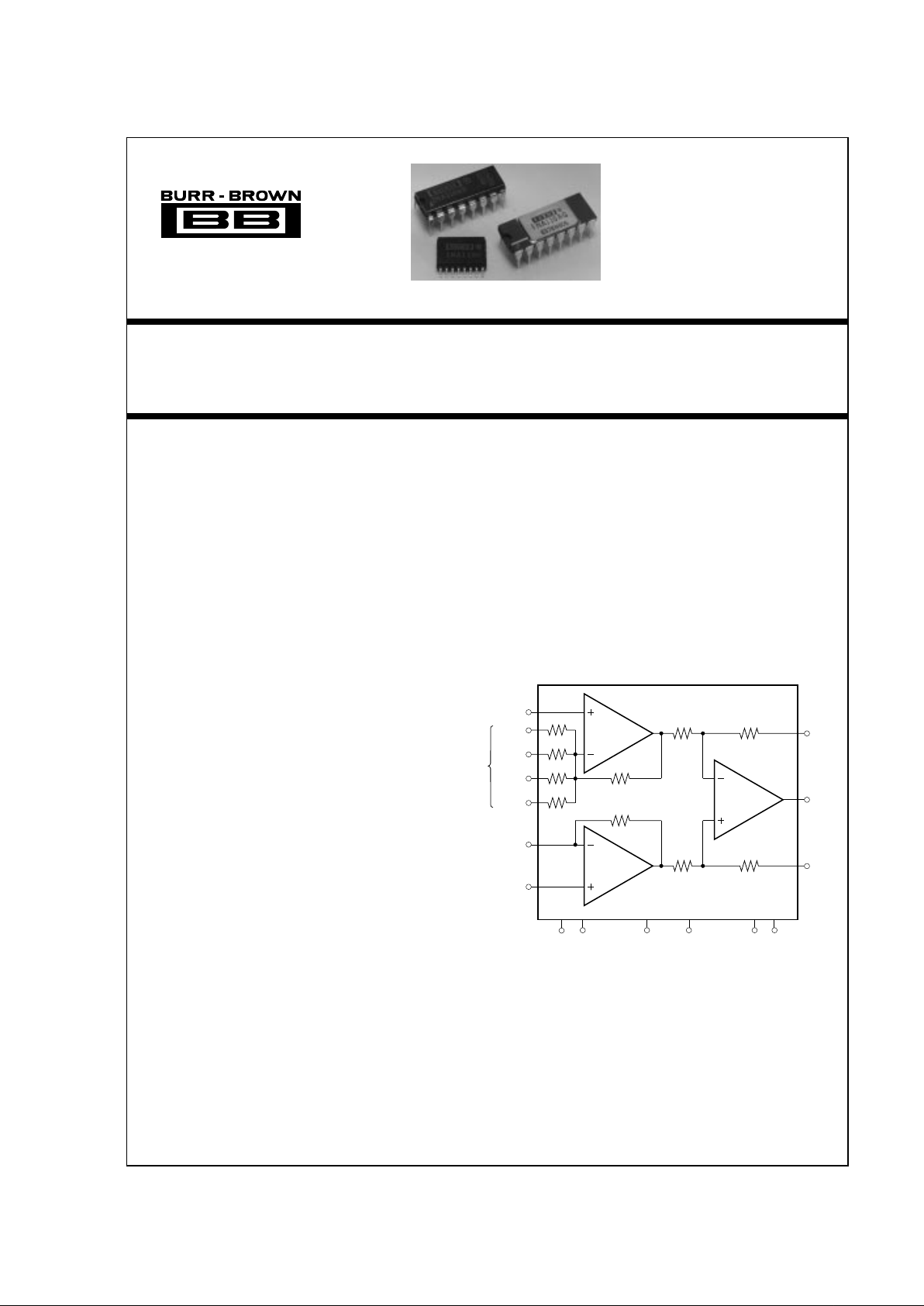
The INA110 is a versatile monolithic FET-input
instrumentation amplifier. Its current-feedback circuit
topology and laser trimmed input stage provide
excellent dynamic performance and accuracy. The
INA110 settles in 4µs to 0.01%, making it ideal for
high speed or multiplexed-input data acquisition
systems.
Internal gain-set resistors are provided for gains of 1,
10, 100, 200, and 500V/V. Inputs are protected for
differential and common-mode voltages up to ±V
CC
.
Its very high input impedance and low input bias
current make the INA110 ideal for applications
requiring input filters or input protection circuitry.
The INA110 is available in 16-pin plastic and ceramic
DIPs, and in the SOL-16 surface-mount package.
Military, industrial and commercial temperature range
grades are available.
A
1
1
404Ω
4.44kΩ
201Ω
80.2Ω
A
2
20kΩ
10kΩ
10kΩ
20kΩ
A
3
10kΩ
10kΩ
13
12
16
11
3
2
4 5 8 7 14 15
9
6
10
–In
X 10
X 100
X 200
X 500
R
G
+In
(1)
Output
Ref
Sense
+V
CC
–V
CC
Input
Offset
Adjust
Output
Offset
Adjust
FET
Input
FET
Input
INA110
NOTE: (1) Connect to R
G
for desired gain.
International Airport Industrial Park • Mailing Address: PO Box 11400 • Tucson, AZ 85734 • Street Address: 6730 S. Tucson Blvd. • Tucson, AZ 85706
Tel: (520) 746-1111 • Twx: 910-952-1111 • Cable: BBRCORP • Telex: 066-6491 • FAX: (520) 889-1510 • Immediate Product Info: (800) 548-6132
®
FEATURES
● LOW BIAS CURRENT: 50pA max
● FAST SETTLING: 4
µs to 0.01%
● HIGH CMR: 106dB min; 90dB at 10kHz
● INTERNAL GAINS: 1, 10, 100, 200, 500
● VERY LOW GAIN DRIFT: 10 to 50ppm/
°C
● LOW OFFSET DRIFT: 2
µV/°C
● LOW COST
● PINOUT SIMILAR TO AD524 AND AD624
©
1986 Burr-Brown Corporation PDS-645E Printed in U.S.A. September, 1993
®
INA110
2
SPECIFICATIONS
ELECTRICAL
At +25°C, ±VCC = 15VDC, and RL = 2kΩ, unless otherwise specified.
INA110BG, SG INA110KP, KUINA110AG
G = 1 + [40k/(RG + 50Ω)]
PARAMETER CONDITIONS MIN TYP MAX MIN TYP MAX MIN TYP MAX UNITS
GAIN
Range of Gain 1 800 * * * * V/V
Gain Equation
(1)
* * V/V
Gain Error, DC: G = 1 0.002 0.04 * 0.02 * * %
G = 10 0.01 0.1 0.005 0.05 * * %
G = 100 0.02 0.2 0.01 0.1 * * %
G = 200 0.04 0.4 0.02 0.2 * * %
G = 500 0.1 1 0.05 0.5 * * %
Gain Temp. Coefficient: G = 1 ±3 ±20 * ±10 * ppm/°C
G = 10 ±4 ±20 ±2 ±10 * ppm/°C
G = 100 ±6 ±40 ±3 ±20 * ppm/°C
G = 200 ±10 ±60 ±5 ±30 * ppm/°C
G = 500 ±25 ±100 ±10 ±50 * ppm/°C
Nonlinearity, DC: G = 1 ±0.001 ±0.01 ±0.0005 ±0.005 * * % of FS
G = 10 ±0.002 ±0.01 ±0.001 ±0.005 * * % of FS
G = 100 ±0.004 ±0.02 ±0.002 ±0.01 * * % of FS
G = 200 ±0.006 ±0.02 ±0.003 ±0.01 * * % of FS
G = 500 ±0.01 ±0.04 ±0.005 ±0.02 * * % of FS
OUTPUT
Voltage, R
L
= 2kΩ Over Temperature ±10 ±12.7 * * * * V
Current Over Temperature ±5 ±25 * * * * mA
Short-Circuit Current ±25 * * mA
Capacitive Load Stability 5000 * * pF
INPUT OFFSET VOLTAGE
(2)
Initial Offset: G, P ±(100 + ±(500 + ±(50 + ±(250 + * * µV
1000/G) 5000/G) 600/G) 3000/G)
U ±(200 + ±(1000 + µV
2000/G) 5000/G)
vs Temperature ±(2 + ±(5 + ±(1 + ±(2 + * µV/°C
20/G) 100/G) 10/G) 50/G)
vs Supply V
CC
= ±6V to ±18V ±(4 + ±(30 + ±(2 + ±(10 + * * µV/V
60/G) 300/G) 30/G) 180/G)
BIAS CURRENT
Initial Bias Current Each Input 20 100 10 50 * * pA
Initial Offset Current 2 50 1 25 * * pA
Impedance: Differential 5x10
12
||6 * * Ω || pF
Common-Mode 2x10
12
||1 * * Ω || pF
VOLTAGE RANGE V
IN
Diff. = 0V
(3)
Range, Linear Response ±10 ±12 * * V
CMR with 1kΩ Source Imbalance:
G = 1 DC 70 90 80 100 * * dB
G = 10 DC 87 104 96 112 * * dB
G = 100 DC 100 110 106 116 * * dB
G = 200 DC 100 110 106 116 * * dB
G = 500 DC 100 110 106 116 * * dB
INPUT NOISE
(4)
Voltage, fO = 10kHz 10 * * nV/√Hz
f
B
= 0.1Hz to 10Hz 1 * * µVp-p
Current, f
O
= 10kHz 1.8 * * fA/√Hz
OUTPUT NOISE
(4)
Voltage, fO = 10kHz 65 * * nV/√Hz
f
B
= 0.1Hz to 10Hz 8 * * µVp-p
DYNAMIC RESPONSE
Small Signal: G = 1 –3dB 2.5 * * MHz
G = 10 2.5 * * MHz
G = 100 470 * * kHz
G = 200 240 * * kHz
G = 500 100 * * kHz
Full Power V
OUT
= ±10V,
G = 2 to 100 190 270 * * * * kHz
Slew Rate G = 2 to 100 12 17 * * * * V/µs
Settling Time:
0.1%, G = 1 V
O
= 20V Step 4 * * µs
G = 10 2 * * µs
G = 100 3 * * µs
G = 200 5 * * µs
G = 500 11 * * µs
®
INA110
3
PARAMETER CONDITIONS MIN TYP MAX MIN TYP MAX MIN TYP MAX UNITS
DYNAMIC RESPONSE (CONT)
Settling Time:
0.01%,G = 1 V
O
= 20V Step 5 12.5 * * * µs
G = 10 3 7.5 * * * µs
G = 100 4 7.5 * * * µs
G = 200 7 12.5 * * * µs
G = 500 16 25 * * * µs
Recovery
(5)
50% Overdrive 1 * * µs
POWER SUPPLY
Rated Voltage ±15 * * V
Voltage Range ±6 ±18 * * * * V
Quiescent Current V
O
= 0V ±3 ±4.5 ** **mA
TEMPERATURE RANGE
Specification: A, B, K –25 +85 * * 0 +70 °C
S –55 +125 °C
Operation –55 +125 * * –25 +85 °C
Storage –65 +150 * * –40 +85 °C
θ
JA
100 * * °C/W
SPECIFICATIONS (CONT)
ELECTRICAL
At +25°C, ±VCC 15VDC, and RL = 2KΩ, unless otherwise specified.
INA110BG, SG INA110KP, KUINA110AG
* Same as INA110AG.
NOTES: (1) Gains other than 1, 10, 100, 200, and 500 can be set by adding an external resistor, R
G
, between pin 3 and pins 11, 12 and 16. Gain accuracy is a function
of R
G
and the internal resistors which have a ±20% tolerance with 20ppm/°C drift. (2) Adjustable to zero. (3) For differential input voltage other than zero, see Typical
Performance Curves. (4) V
NOISE RTI
= √V
N
2
INPUT
+ (V
N OUTPUT
/Gain)2. (5) Time required for output to return from saturation to linear operation following the removal of
an input overdrive voltage.
ABSOLUTE MAXIMUM RATINGS
Supply Voltage.................................................................................. ±18V
Input Voltage Range .......................................................................... ±V
CC
Operating Temperature Range: G ................................. –55°C to +125°C
P, U............................... –25°C to +85°C
Storage Temperature Range: G .................................... –65°C to +150°C
P, U.................................. –40°C to +85°C
Lead Temperature (soldering, 10s): G, P ..................................... +300°C
(soldering, 3s): U ........................................... +260°C
Output Short Circuit Duration ............................... Continuous to Common
PACKAGE INFORMATION
PACKAGE DRAWING
MODEL PACKAGE NUMBER
(1)
INA110AG 16-Pin Ceramic DIP 109
INA110BG 16-Pin Ceramic DIP 109
INA110SG 16-Pin Ceramic DIP 109
INA110KP 16-Pin Plastic DIP 180
INA110KU SOL-16 SOIC 211
NOTE: (1) For detailed drawing and dimension table, please see end of data
sheet, or Appendix D of Burr-Brown IC Data Book.
Top View DIP/SOIC
PIN CONFIGURATION
ORDERING INFORMATION
MODEL PACKAGE TEMPERATURE RANGE
INA110AG 16-Pin Ceramic DIP –25°C to +85°C
INA110BG 16-Pin Ceramic DIP –25°C to +85°C
INA110SG 16-Pin Ceramic DIP –55°C to +125°C
INA110KP 16-Pin Plastic DIP 0°C to +70°C
INA110KU SOL-16 SOIC 0°C to +70°C
The information provided herein is believed to be reliable; however, BURR-BROWN assumes no responsibility for inaccuracies or omissions. BURR-BROWN
assumes no responsibility for the use of this information, and all use of such information shall be entirely at the user’s own risk. Prices and specifications are subject
to change without notice. No patent rights or licenses to any of the circuits described herein are implied or granted to any third party. BURR-BROWN does not
authorize or warrant any BURR-BROWN product for use in life support devices and/or systems.
–In
+In
R
G
Input Offset Adj.
Input Offset Adj.
Reference
–V
CC
+V
CC
x200
Output Offset Adj.
Output Offset Adj.
x10
x100
x500
Output Sense
Output
1
2
3
4
5
6
7
8
16
15
14
13
12
11
10
9
®
INA110
4
0
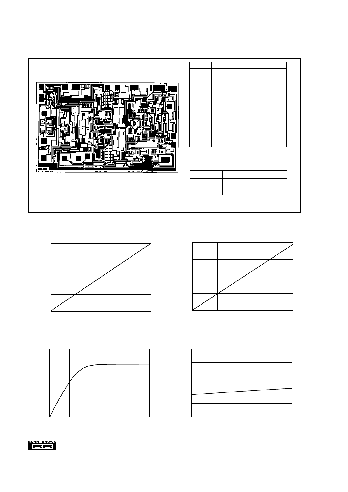
Load Resistance (Ω)
OUTPUT SWING vs LOAD RESISTANCE
Output Voltage (V)
±16
±12
±8
±4
400 1.6k02M800 1.2k
±4
Power Supply Voltage (V)
OUTPUT SWING vs SUPPLY
Output Voltage (V)
±16
±13
±10
±7
RL = 2kΩ
±9 ±15±6 ±18±12
±3
Power Supply Voltage (V)
INPUT VOLTAGE RANGE vs SUPPLY
Input Voltage Range (V)
±9 ±15±6 ±18
±15
±12
±9
±6
±12
0
Power Supply Voltage (V)
BIAS CURRENT vs SUPPLY
Input Bias Current (pA)
±9 ±15±6 ±18
25
20
15
10
5
±12
DICE INFORMATION
PAD FUNCTION
1 –In
2 +In
3A,3B R
G
(connect both)
4 Input Offset Adjust
5 Input Offset Adjust
6 Reference
7–V
CC
8+V
CC
9 Output
10 Output Sense
11 x500
12 x100
13 x10
14 Output Offset Adjust
15 Output Offset Adjust
16 x200
Pads 3A and 3B must be connected.
Substrate Bias: Internally connected to –V
CC
power sup-
ply.
MECHANICAL INFORMATION
MILS (0.001") MILLIMETERS
Die Size 139 x 89 ±5 3.53 x 2.26 ±0.13
Die Thickness 20 ±3 0.51 ±0.08
Min. Pad Size 4 x 4 0.10 x 0.10
Backing Gold
TYPICAL PERFORMANCE CURVES
At TA = +25°C, and ±VCC = 15VDC, unless otherwise noted.
INA110 DIE TOPOGRAPHY
15 14 13 12 11
10
9
8
7
7
6
5
4
3A
2
1
16
3B
 Loading...