

Burr Brown INA106U, INA106KP Datasheet
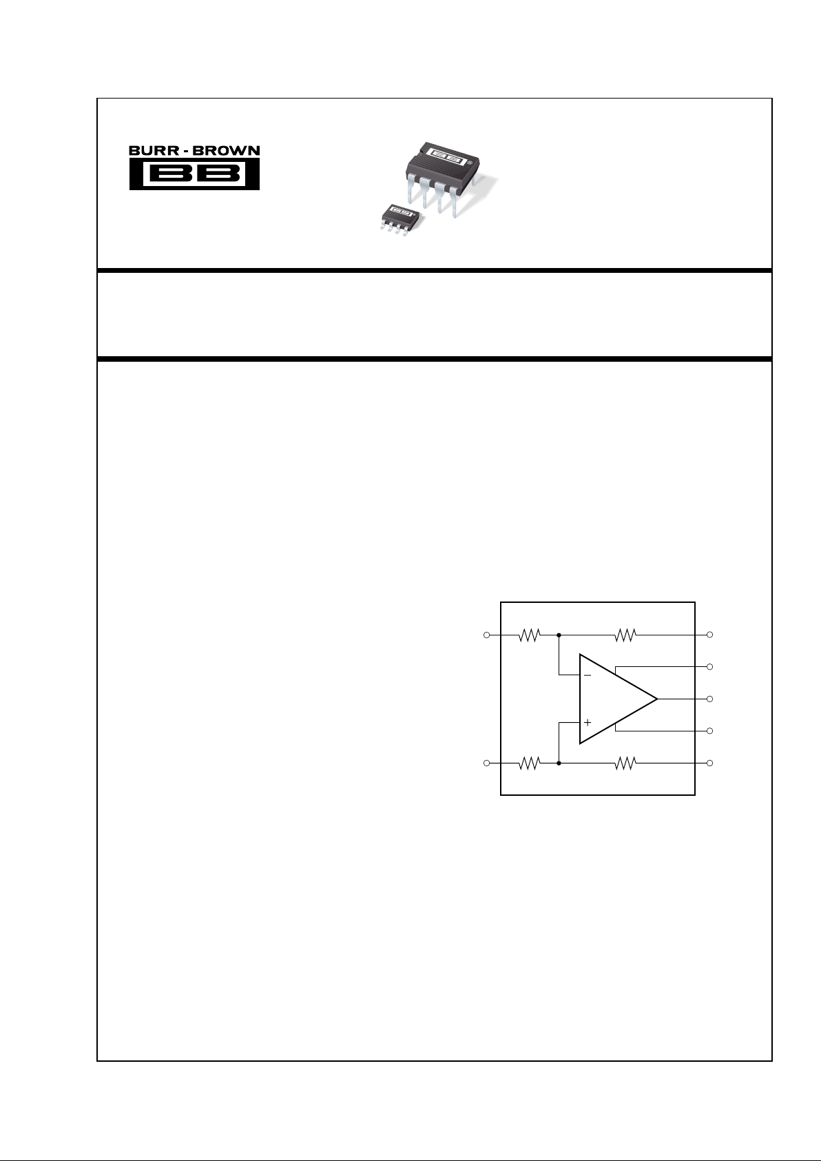
R
2
100kΩ
R
1
10kΩ
2
3
–In
+In
R
4
100kΩ
R
3
10kΩ
5
1
Sense
Reference
4
V–
6
Output
7
V+
Precision Gain = 10
DIFFERENTIAL AMPLIFIER
APPLICATIONS
● G = 10 DIFFERENTIAL AMPLIFIER
● G = +10 AMPLIFIER
● G = –10 AMPLIFIER
● G = +11 AMPLIFIER
● INSTRUMENTATION AMPLIFIER
DESCRIPTION
The INA106 is a monolithic Gain = 10 differential
amplifier consisting of a precision op amp and on-chip
metal film resistors. The resistors are laser trimmed
for accurate gain and high common-mode rejection.
Excellent TCR tracking of the resistors maintains
gain accuracy and common-mode rejection over
temperature.
The differential amplifier is the foundation of many
commonly used circuits. The INA106 provides this
precision circuit function without using an expensive
resistor network. The INA106 is available in 8-pin
plastic DIP and SO-8 surface-mount packages.
®
FEATURES
● ACCURATE GAIN: ±0.025% max
● HIGH COMMON-MODE REJECTION:
86dB min
● NONLINEARITY: 0.001% max
● EASY TO USE
● PLASTIC 8-PIN DIP, SO-8 SOIC
PACKAGES
INA106
International Airport Industrial Park • Mailing Address: PO Box 11400, Tucson, AZ 85734 • Street Address: 6730 S. Tucson Blvd., Tucson, AZ 85706 • Tel: (520) 746-1111 • Twx: 910-952-1111
Internet: http://www.burr-brown.com/ • FAXLine: (800) 548-6133 (US/Canada Only) • Cable: BBRCORP • Telex: 066-6491 • FAX: (520) 889-1510 • Immediate Product Info: (800) 548-6132
INA106
INA106
©
1987 Burr-Brown Corporation PDS-729F Printed in U.S.A. August, 1998

®
INA106
2
INA106KP, U
PARAMETER CONDITIONS MIN TYP MAX UNITS
GAIN
Initial
(1)
10 V/V
Error 0.01 0.025 %
vs Temperature –4 ppm/°C
Nonlinearity
(2)
0.0002 0.001 %
OUTPUT
Related Voltage I
O
= +20mA, –5mA 10 12 V
Rated Current V
O
= 10V +20, –5 mA
Impedance 0.01 Ω
Current Limit To Common +40/–10 mA
Capacitive Load Stable Operation 1000 pF
INPUT
Impedance Differential 10 kΩ
Common-Mode 110 kΩ
Voltage Range Differential ±1V
Common-Mode ±11 V
Common-Mode Rejection
(3)
TA = T
MIN
to T
MAX
86 100 dB
OFFSET VOLTAGE RTI
(4)
Initial 50 200 µV
vs Temperature 0.2 µV/°C
vs Supply ±V
S
= 6V to 18V 1 10 µV/V
vs Time 10 µV/mo
NOISE VOLTAGE RTI
(5)
fB = 0.01Hz to 10Hz 1 µVp-p
f
O
= 10kHz 30 nV/√Hz
DYNAMIC RESPONSE
Small Signal –3dB 5 MHz
Full Power BW V
O
= 20Vp-p 30 50 kHz
Slew Rate 23 V/µs
Settling Time: 0.1% V
O
= 10V Step 5 µs
0.01% V
O
= 10V Step 10 µs
0.01% V
CM
= 10V Step, V
DIFF
= 0V 5 µs
POWER SUPPLY
Rated ±15 V
Voltage Range Derated Performance ±5 ±18 V
Quiescent Current V
O
= 0V ±1.5 ±2mA
TEMPERATURE RANGE
Specification 0 +70 °C
Operation –40 +85 °C
Storage –65 +150 °C
SPECIFICATIONS
ELECTRICAL
At +25°C, VS = ±15V, unless otherwise specified.
NOTES: (1) Connected as difference amplifier (see Figure 1). (2) Nonlinearity is the maximum peak deviation from the best-fit straight line as a percent of full-scale peakto-peak output. (3) With zero source impedance (see “Maintaining CMR” section). (4) Includes effects of amplifiers’s input bias and offset currents. (5) Includes effect
of amplifier’s input current noise and thermal noise contribution of resistor network.
 Loading...