

Page 1
®
INA106
INA106
Precision Gain = 10
DIFFERENTIAL AMPLIFIER
INA106
FEATURES
● ACCURATE GAIN: ±0.025% max
● HIGH COMMON-MODE REJECTION:
86dB min
● NONLINEARITY: 0.001% max
● EASY TO USE
● PLASTIC 8-PIN DIP, SO-8 SOIC
PACKAGES
DESCRIPTION
The INA106 is a monolithic Gain = 10 differential
amplifier consisting of a precision op amp and on-chip
metal film resistors. The resistors are laser trimmed
for accurate gain and high common-mode rejection.
Excellent TCR tracking of the resistors maintains
gain accuracy and common-mode rejection over
temperature.
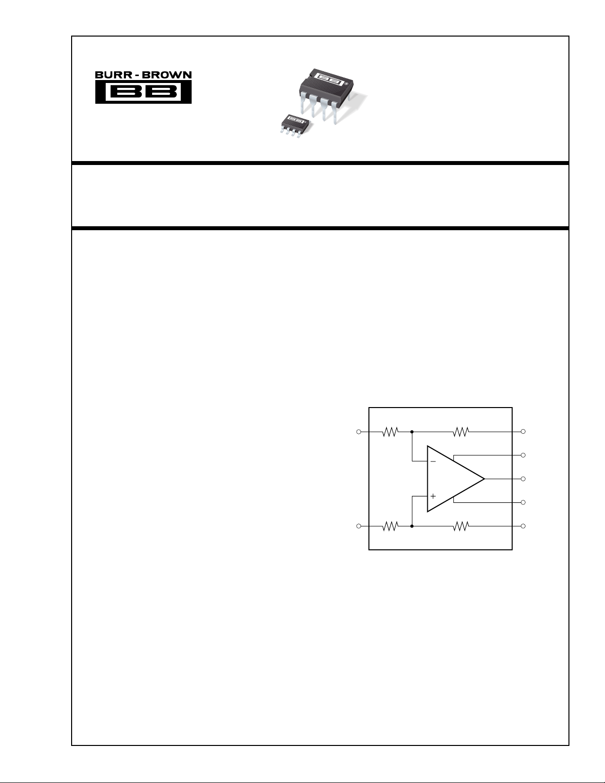
The differential amplifier is the foundation of many
commonly used circuits. The INA106 provides this
precision circuit function without using an expensive
resistor network. The INA106 is available in 8-pin
plastic DIP and SO-8 surface-mount packages.
APPLICATIONS
● G = 10 DIFFERENTIAL AMPLIFIER
● G = +10 AMPLIFIER
● G = –10 AMPLIFIER
● G = +11 AMPLIFIER
● INSTRUMENTATION AMPLIFIER
R
2
100kΩ
R
4
100kΩ
–In
+In
R
1
10kΩ
2
R
3
10kΩ
3
5
7
6
4
1
Sense
V+
Output
V–
Reference
SBOS152
International Airport Industrial Park • Mailing Address: PO Box 11400, Tucson, AZ 85734 • Street Address: 6730 S. Tucson Blvd., Tucson, AZ 85706 • Tel: (520) 746-1111 • Twx: 910-952-1111
Internet: http://www.burr-brown.com/ • FAXLine: (800) 548-6133 (US/Canada Only) • Cable: BBRCORP • Telex: 066-6491 • FAX: (520) 889-1510 • Immediate Product Info: (800) 548-6132
©
1987 Burr-Brown Corporation PDS-729F Printed in U.S.A. August, 1998
Page 2

SPECIFICATIONS
ELECTRICAL
At +25°C, VS = ±15V, unless otherwise specified.
INA106KP, U
PARAMETER CONDITIONS MIN TYP MAX UNITS
GAIN
(1)
Initial
Error 0.01 0.025 %
vs Temperature –4 ppm/°C
Nonlinearity
(2)
OUTPUT
Related Voltage I
Rated Current V
Impedance 0.01 Ω
= +20mA, –5mA 10 12 V
O
= 10V +20, –5 mA
O
Current Limit To Common +40/–10 mA
Capacitive Load Stable Operation 1000 pF
INPUT
Impedance Differential 10 kΩ
Common-Mode 110 kΩ
Voltage Range Differential ±1V
Common-Mode Rejection
(3)
OFFSET VOLTAGE RTI
Common-Mode ±11 V
TA = T
MIN
to T
(4)
MAX
86 100 dB
Initial 50 200 µV
vs Temperature 0.2 µV/°C
vs Supply ±V
vs Time 10 µV/mo
NOISE VOLTAGE RTI
= 6V to 18V 1 10 µV/V
S
(5)
fB = 0.01Hz to 10Hz 1 µVp-p
f
= 10kHz 30 nV/√Hz
O
DYNAMIC RESPONSE
Small Signal –3dB 5 MHz
Full Power BW V
Slew Rate 23 V/µs
Settling Time: 0.1% V
0.01% V
0.01% V
= 20Vp-p 30 50 kHz
O
= 10V Step 5 µs
O
= 10V Step 10 µs
O
= 10V Step, V
CM
= 0V 5 µs
DIFF
POWER SUPPLY
Rated ±15 V
Voltage Range Derated Performance ±5 ±18 V
Quiescent Current V
= 0V ±1.5 ±2mA
O
TEMPERATURE RANGE
Specification 0 +70 °C
Operation –40 +85 °C
Storage –65 +150 °C
NOTES: (1) Connected as difference amplifier (see Figure 1). (2) Nonlinearity is the maximum peak deviation from the best-fit straight line as a percent of full-scale peakto-peak output. (3) With zero source impedance (see “Maintaining CMR” section). (4) Includes effects of amplifiers’s input bias and offset currents. (5) Includes effect
of amplifier’s input current noise and thermal noise contribution of resistor network.
10 V/V
0.0002 0.001 %
®
INA106
2
Page 3
PIN CONFIGURATION
Top View DIP/SOIC
(1)
Ref
–In
+In
V–
NOTE: (1) Pin 1 indentifier for SO-8 package.
Model number identification may be abbreviated
on SO-8 package due to limited available space.
•
18
10kΩ
2
10kΩ
3
4
100kΩ
100kΩ
INA106
NC
7
V+
6
Output
5
Sense
ABSOLUTE MAXIMUM RATINGS
Power Supply Voltage ...................................................................... ±18V
Input Voltage Range ............................................................................±V
Operating Temperature Range: P, U ................................–40°C to +85°C
Storage Temperature Range ............................................–40°C to +85°C
Lead Temperature (soldering, 10s): P ..........................................+300°C
Wave Soldering (3s, max) U ..........................................................+260°C
Output Short Circuit to Common..............................................Continuous
ELECTROSTATIC
DISCHARGE SENSITIVITY
This integral circuit can be damaged by ESD. Burr-Brown
recommends that all integrated circuits be handled with
appropriate precautions. Failure to observe proper handling
and installation procedures can cause damage.
ESD damage can range from subtle performance degradation to complete device failure. Precision integrated circuits
may be more susceptible to damage because very small
parametric changes could cause the device not to meet
published specifications.
PACKAGE/ORDERING INFORMATION
PACKAGE
DRAWING TEMPERATURE
PRODUCT PACKAGE NUMBER
INA106KP 8-Pin Plastic DIP 006 0°C to +70°C
S
INA106U SO-8 Surface Mount 182 0°C to +70°C
NOTE: (1) For detailed drawing and dimension table, please see end of data
sheet, or Appendix C of Burr-Brown IC Data Book.
(1)
RANGE
The information provided herein is believed to be reliable; however, BURR-BROWN assumes no responsibility for inaccuracies or omissions. BURR-BROWN
assumes no responsibility for the use of this information, and all use of such information shall be entirely at the user’s own risk. Prices and specifications are subject
to change without notice. No patent rights or licenses to any of the circuits described herein are implied or granted to any third party. BURR-BROWN does not
authorize or warrant any BURR-BROWN product for use in life support devices and/or systems.
3
INA106
®
Page 4

TYPICAL PERFORMANCE CURVES
At TA = +25°C, VS = ±15V, unless otherwise noted.
STEP RESPONSE
SMALL SIGNAL RESPONSE
(No Load)
50
0
Output Voltage (mV)
–50
50
0
Output Voltage (mV)
–50
–17.5
–15
–12.5
–10
(V)
OUT
–7.5
V
–5
–2.5
0
0
2µs/div
SMALL SIGNAL RESPONSE
= ∞, C
(R
LOAD
LOAD
= 100pF)
2µs/div
MAXIMUM V
(Negative Swing)
OUT
vs I
OUT
VS = ±18V
VS = ±15V
VS = ±12V
VS = ±5V
–2 –4 –6 –8 –10 –12
(mA)
–I
OUT
2µs/div
TOTAL HARMONIC DISTORTION AND NOISE
vs FREQUENCY
1
A = 20dB, 3Vrms, 10kΩ load
0.1
THD + N (%)
0.01
Noninverting
30kHz low-pass filtered
0.001
1k 10k 100k
Frequency (Hz)
MAXIMUM V
(Positive Swing)
OUT
vs I
OUT
17.5
15
VS = ±18V
12.5
VS = ±15V
10
(V)
V
OUT
7.5
VS = ±12V
5
2.5
0
0
VS = ±5V
6 1218243036
I
(mA)
OUT
Inverting
®
INA106
4
Page 5

TYPICAL PERFORMANCE CURVES (CONT)
At TA = +25°C, VS = ±15V, unless otherwise noted.
110
100
90
80
CMR (dB)
70
60
10
CMR vs FREQUENCY
100 1k 10k 100k
Frequency (Hz)
APPLICATIONS INFORMATION
Figure 1 shows the basic connections required for operation
of the INA106. Power supply bypass capacitors should be
connected close to the device pins as shown.
V–
1µF
47
INA106
R
1
10kΩ
25
V
2
R
3
10kΩ
3
V
3
100kΩ
R
4
100kΩ
V+
1µF
R
2
6
+
= 10(V3 –V2)
V
OUT
–
POWER SUPPLY REJECTION
140
120
100
80
PSRR (dB)
60
40
1
10 100 1k 10k 100k
vs FREQUENCY
V–
V+
Frequency (Hz)
Ref terminal will be summed with the output signal. The
source impedance of a signal applied to the Ref terminal
should be less than 10Ω to maintain good common-mode
rejection.
Figure 2 shows a voltage applied to pin 1 to trim the offset
voltage of the INA106. The known 100Ω source impedance
of the trim circuit is compensated by the 10Ω resistor in
series with pin 3 to maintain good CMR.
INA106
R
V
2
V
3
25
10Ω
3
1
R
3
R
2
6
V
O
1
FIGURE 1. Basic Power Supply and Signal Connections.
The differential input signal is connected to pins 2 and 3 as
shown. The source impedance connected to the inputs must
be equal to assure good common-mode rejection. A 5Ω
mismatch in source impedance will degrade the commonmode rejection of a typical device to approximately 86dB. If
the source has a known source impedance mismatch, an
additional resistor in series with one input can be used to
preserve good common-mode rejection.
The output is referred to the output reference terminal
(pin 1) which is normally grounded. A voltage applied to the
Compensates for
some impedance
at pin 1. See text.
= V2 – V
V
Offset Adjustment Range = ±3mV
O
3
1
R
4
100Ω
+15V
499kΩ
–15V
FIGURE 2. Offset Adjustment.
Referring to Figure 1, the CMR depends upon the match of
the internal R4/R3 ratio to the R1/R2 ratio. A CMR of 106dB
requires resistor matching of 0.005%. To maintain high
CMR over temperature, the resistor TCR tracking must be
better than 2ppm/°C. These accuracies are difficult and
expensive to reliably achieve with discrete components.
5
INA106
100kΩ
®
Page 6

10Ω 10kΩ 100kΩ
V
1
2
INA106
E
1
–In
5
200Ω
Gain
Adjust
A
1
R
2
2
INA106
5
E
6
10Ω
V
2
10kΩ 100kΩ
3
1
200Ω
0
CMR
Adjust
To eliminate adjustment interactions,
first adjust gain with V2 grounded.
FIGURE 3. Difference Amplifier with Gain and CMR Adjust.
INA106
10kΩ 100kΩ
25
V
2
6
V
O
10kΩ 100kΩ
3
1
VO = –10V
2
6
1
E
0
Output
E
+In
R
1
R
2
3
A
2
2
= 10(1 + 2R2 /R1) (E2 – E1)
E
0
To make a high performance high gain instrumentation amplifier, the INA106
can be combined with state-of-the-art op amps. For low source impedance
applications, OPA37s will give the best noise, offset, and temperature drift. At
source impedances above about 10kΩ, the bias current noise of the OPA37
reacting with input impedance degrades noise. For these applications, use an
OPA111 or a dual OPA2111 FET input op amp for lower noise. For an
electrometer grade IA, use the OPA128—see table below.
Using the INA106 for the difference amplifier also extends the input commonmode range of the instrumentation amplifier to ±10V. A conventional IA with
a unity-gain difference amplifier has an input common-mode range limited to
±5V for an output swing of ±10V. This is because a unity-gain difference amp
needs ±5V at the input for 10V at the output, allowing only 5V additional for
common-mode.
R1R2GAIN CMRR NOISE AT 1kHz
A
, A
1
2
(Ω)(kΩ) (V/V) (dB) Ib (pA) (nV/ √Hz)
OPA37A 50.5 2.5 1000 128 40000 4
OPA111B 202 10 1000 110 1 10
OPA128LM 202 10 1000 118 0.075 38
Gain Error = 0.01% maximum
Nonlinearity = 0.001% maximum
Gain Drift = 2.ppm/°C
FIGURE 4. Precision G = –10 Inverting Amplifier.
INA106
R
1
10kΩ
25
R
4
V
IN
100kΩ
1
±100V
Safe Input
This circuit follows an 11/1 divider with a gain of 11 for an overall gain of unity.
With an 11/1 divider, the input signal can exceed 100V without damage.
3
R
10kΩ
R
100kΩ
3
2
V
O
6
V
= V
O
IN
FIGURE 5. Voltage Follower with Input Protection.
FIGURE 6. Precision Instrumentation Amplifier.
INA106
R
1
10kΩ
25
R
4
V
V
100kΩ
1
1
R
3
3
10kΩ
3
R
2
100kΩ
V
0
6
V0 = V1 + 10 V
FIGURE 7. Precision Summing Amplifier.
INA106
1
V
IN
3
2
5
6
V
O
Gain Error =
0.01% maximum
V
= 11V
3
O
IN
®
INA106
FIGURE 8. Precision G = 11 Buffer.
6
Page 7

IMPORTANT NOTICE
T exas Instruments and its subsidiaries (TI) reserve the right to make changes to their products or to discontinue
any product or service without notice, and advise customers to obtain the latest version of relevant information
to verify, before placing orders, that information being relied on is current and complete. All products are sold
subject to the terms and conditions of sale supplied at the time of order acknowledgment, including those
pertaining to warranty, patent infringement, and limitation of liability.
TI warrants performance of its semiconductor products to the specifications applicable at the time of sale in
accordance with TI’s standard warranty. T esting and other quality control techniques are utilized to the extent
TI deems necessary to support this warranty . Specific testing of all parameters of each device is not necessarily
performed, except those mandated by government requirements.
Customers are responsible for their applications using TI components.
In order to minimize risks associated with the customer’s applications, adequate design and operating
safeguards must be provided by the customer to minimize inherent or procedural hazards.
TI assumes no liability for applications assistance or customer product design. TI does not warrant or represent
that any license, either express or implied, is granted under any patent right, copyright, mask work right, or other
intellectual property right of TI covering or relating to any combination, machine, or process in which such
semiconductor products or services might be or are used. TI’s publication of information regarding any third
party’s products or services does not constitute TI’s approval, warranty or endorsement thereof.
Copyright 2000, Texas Instruments Incorporated
 Loading...