

Page 1
D
R
V
1
3
4
DRV135
D
R
V
1
3
4
SBOS094A – JANUARY 1998 – REVISED APRIL 2007
AUDIO BALANCED LINE DRIVERS
DRV134
DRV135
FEATURES
● BALANCED OUTPUT
● LOW DISTORTION: 0.0005% at f = 1kHz
● WIDE OUTPUT SWING: 17Vrms into 600Ω
● HIGH CAPACITIVE LOAD DRIVE
● HIGH SLEW RATE: 15V/
● WIDE SUPPLY RANGE:
µs
±4.5V to ±18V
● LOW QUIESCENT CURRENT: ±5.2mA
● 8-PIN DIP, SO-8, AND SOL-16 PACKAGES
● COMPANION TO AUDIO DIFFERENTIAL
LINE RECEIVERS: INA134 and INA137
● IMPROVED REPLACEMENT FOR SSM2142
APPLICATIONS
● AUDIO DIFFERENTIAL LINE DRIVERS
● AUDIO MIX CONSOLES
● DISTRIBUTION AMPLIFIERS
● GRAPHIC/PARAMETRIC EQUALIZERS
● DYNAMIC RANGE PROCESSORS
● DIGITAL EFFECTS PROCESSORS
● TELECOM SYSTEMS
● HI-FI EQUIPMENT
● INDUSTRIAL INSTRUMENTATION
DESCRIPTION
The DRV134 and DRV135 are differential output amplifiers that convert a single-ended input to a balanced
output pair. These balanced audio drivers consist of
high performance op amps with on-chip precision resistors. They are fully specified for high performance audio
applications and have excellent ac specifications, including low distortion (0.0005% at 1kHz) and high slew
rate (15V/µs).
The on-chip resistors are laser-trimmed for accurate gain
and optimum output common-mode rejection. Wide output
voltage swing and high output drive capability allow use in
a wide variety of demanding applications. They easily drive
the large capacitive loads associated with long audio
cables. Used in combination with the INA134 or INA137
differential receivers, they offer a complete solution for
transmitting analog audio signals without degradation.
The DRV134 is available in 8-pin DIP and SOL-16 surface-mount packages. The DRV135 comes in a spacesaving SO-8 surface-mount package. Both are specified
for operation over the extended industrial temperature
range, –40°C to +85°C and operate from –55°C to +125°C.
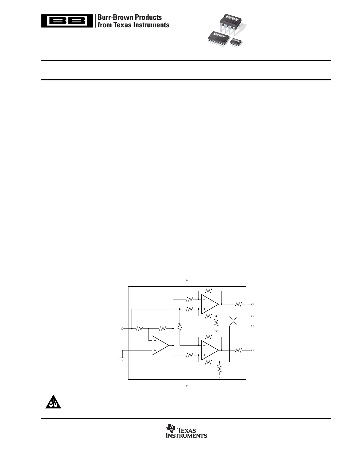
V+
A2
V
IN
Gnd
All resistors 30kΩ unless otherwise indicated.
Please be aware that an important notice concerning availability, standard warranty, and use in critical applications of
Texas Instruments semiconductor products and disclaimers thereto appears at the end of this data sheet.
All trademarks are the property of their respective owners.
PRODUCTION DATA information is current as of publication date.
Products conform to specifications per the terms of Texas Instruments
standard warranty. Production processing does not necessarily include
testing of all parameters.
A1
A3
V–
www.ti.com
50Ω
10kΩ
50Ω
10kΩ
Copyright © 1998-2007, Texas Instruments Incorporated
+V
O
+Sense
–Sense
–V
O
Page 2

SPECIFICATIONS: V
= ±18V
S
At TA = +25°C, VS = ±18V, RL = 600Ω differential connected between +VO and –VO, unless otherwise noted.
DRV134PA, UA
DRV135UA
PARAMETER CONDITIONS MIN TYP MAX UNITS
AUDIO PERFORMANCE
Total Harmonic Distortion + Noise THD+N f = 20Hz to 20kHz,VO = 10Vrms 0.001 %
Noise Floor, RTO
Headroom, RTO
INPUT
Input Impedance
Input Current I
(1)
(1)
(2)
Z
IN
IN
GAIN [(+V
Differential VIN = ±10V
f = 1kHz, V
= 10Vrms 0.0005 %
O
20kHz BW –98 dBu
THD+N < 1% +27 dBu
10 kΩ
VIN = ±7.07V ±700 ±1000 µA
) – (–VO)]/V
O
IN
Initial 5.8 6 dB
Error ±0.1 ±2%
vs Temperature ±10 ppm/°C
Single-Ended V
= ±5V
IN
Initial 5.8 6 dB
Error ±0.7 ±2%
vs Temperature ±10 ppm/°C
Nonlinearity 0.0003 % of FS
OUTPUT
Common-Mode Rejection, f = 1kHz OCMR See OCMR Test Circuit, Figure 4 46 68 dB
Signal Balance Ratio, f = 1kHz SBR See SBR Test Circuit, Figure 5 35 54 dB
Output Offset Voltage
Offset Voltage, Common-Mode V
vs Temperature ±150 µV/°C
Offset Voltage, Differential V
OCM
(3)
(4)
OD
VIN = 0 ±50 ±250 mV
VIN = 0 ±1 ±10 mV
vs Temperature ±5 µV/°C
vs Power Supply PSRR V
Output Voltage Swing, Positive No Load
Negative No Load
= ±4.5V to ±18V 80 110 dB
S
(5)
(5)
(V+) – 3 (V+) – 2.5 V
(V–) + 2 (V–) + 1.5 V
Impedance 50 Ω
Load Capacitance, Stable Operation C
Short-Circuit Current I
Tied to Ground (each output) 1 µF
LCL
SC
±85 mA
FREQUENCY RESPONSE
Small-Signal Bandwidth 1.5 MHz
Slew Rate SR 15 V/µs
Settling Time: 0.01% V
= 10V Step 2.5 µs
OUT
Overload Recovery Output Overdriven 10% 3 µs
POWER SUPPLY
Rated Voltage V
S
±18 V
Voltage Range ±4.5 ±18 V
Quiescent Current I
Q
IO = 0 ±5.2 ±5.5 mA
TEMPERATURE RANGE
Specification Range –40 +85 °C
Operation Range –55 +125 °C
Storage Range –55 +125 °C
Thermal Resistance
8-Pin DIP 100 °C/W
θ
JA
SO-8 Surface Mount 150 °C/W
SOL-16 Surface Mount 80 °C/W
NOTES: (1) dBu = 20log (Vrms /0.7746); RTO = Referred-to-Output.
(2) Resistors are ratio matched but have ±20% absolute value.
(3) V
= [(+VO) + (–VO)]/2. (4) VOD = (+VO) – (–VO). (5) Ensures linear operation. Includes common-mode offset.
OCM
2
www.ti.com
DRV134, DRV135
SBOS094A
Page 3
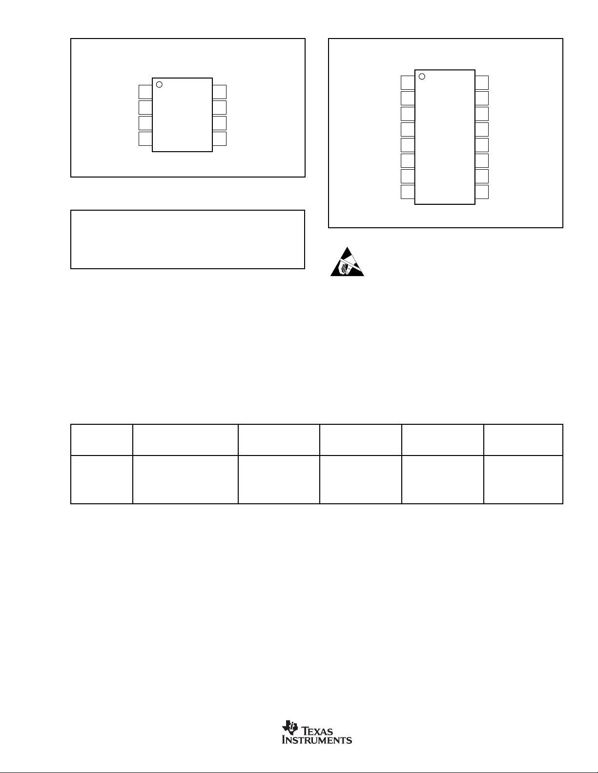
PIN CONFIGURATIONS
Top View 8-Pin DIP/SO-8
1
–V
O
Gnd
V
2
3
4
IN
–Sense
ABSOLUTE MAXIMUM RATINGS
Supply Voltage, V+ to V–.................................................................... 40V
Input Voltage Range .................................................................... V– to V+
Output Short-Circuit (to ground) .............................................. Continuous
Operating Temperature .................................................. –55°C to +125°C
Storage Temperature ..................................................... –55°C to +125°C
Junction Temperature .................................................................... +150°C
NOTE: (1) Stresses above these ratings may cause permanent damage.
Exposure to absolute maximum conditions for extended periods may affect
device reliability.
8
7
6
5
(1)
+V
O
+Sense
V+
V–
Top View SOL-16
NC
NC
–V
–Sense
Gnd
V
NC
NC
1
2
3
O
4
5
6
IN
7
8
NC
16
NC
15
+V
14
O
+Sense
13
V+
12
V–
11
NC
10
NC
9
ELECTROSTATIC
DISCHARGE SENSITIVITY
This integrated circuit can be damaged by ESD. Texas
Instruments recommends that all integrated circuits be
handled with appropriate precautions. Failure to observe proper handling and installation procedures can
cause damage.
ESD damage can range from subtle performance degradation to complete device failure. Precision integrated
circuits may be more susceptible to damage because
very small parametric changes could cause the device
not to meet its published specifications.
PACKAGE/ORDERING INFORMATION
PRODUCT PACKAGE-LEAD DESIGNATOR RANGE NUMBER MEDIA, QUANTITY
DRV134PA DIP-8 P –40°C to +85°C DRV134PA Rails, 50
DRV134UA SOL-16 Surface Mount DW –40°C to +85°C DRV134UA Rails, 48
" " " " DRV134UA/1K Tape and Reel. 1000
DRV135UA SO-8 Surface Mount D –40°C to +85°C DRV135UA Rails, 100
" " " " DRV135UA/2K5 Tape and Reel, 2500
NOTE: (1) For the most current package and ordering information, see the Package Option Addendum at the end of this data sheet, or see the TI wwebsite at www.ti.com.
(1)
SPECIFIED
PACKAGE TEMPERATURE ORDERING TRANSPORT
DRV134, DRV135
SBOS094A
www.ti.com
3
Page 4
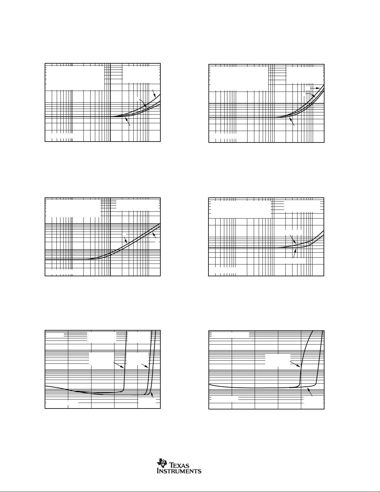
TYPICAL PERFORMANCE CURVES
At TA = +25°C, VS = ±18V, RL = 600Ω differential connected between +VO and –VO, unless otherwise noted.
TOTAL HARMONIC DISTORTION+NOISE
vs FREQUENCY
0.01
See Figure 3 for Test Circuit
A: R
= R2 = RL = ∞ (no load)
1
B: R
= R2 = 600Ω, RL = ∞
1
C: R
= R2 = ∞, RL = 600Ω
1
Differential Mode
0.001
THD+N (%)
0.0001
DRV134 Output
20 100 1k 10k 20k
Frequency (Hz)
TOTAL HARMONIC DISTORTION+NOISE
vs FREQUENCY
0.1
–VO or +VO Grounded
A: R
= 600Ω (250 ft cable)
1
B: R
= ∞ (no cable)
1
Single-Ended Mode
0.01
A
THD+N (%)
0.001
V
= 10Vrms
O
No Cable
C
V
= 10Vrms
O
TOTAL HARMONIC DISTORTION+NOISE
vs FREQUENCY
0.01
See Figure 3 for Test Circuit
A: R
= R2 = RL = ∞ (no load)
1
B: R
= R2 = 600Ω, RL = ∞
1
C: R
A
B
0.001
= R2 = ∞, RL = 600Ω
1
Differential Mode
V
= 10Vrms
O
500 ft cable
A
B
THD+N (%)
C
DRV134 Output
0.0001
20 100 1k 10k 20k
Frequency (Hz)
SYSTEM TOTAL HARMONIC DISTORTION+NOISE
vs FREQUENCY
0.01
See Figure 3 for Test Circuit
A: R
= R2 = RL = ∞ (no load)
1
B: R
= R2 = ∞ RL = 600Ω
1
B
0.001
Differential Mode
V
= 10Vrms
O
A (no cable)
THD+N (%)
0.0001
DRV134 Output
20 100 1k 10k 20k
Frequency (Hz)
HEADROOM—TOTAL HARMONIC DISTORTION+NOISE
vs OUTPUT AMPLITUDE
1
f = 1kHz
Single-Ended
Mode
0.1
500 ft Cable
R
= 600Ω
L
0.01
THD+N (%)
0.001
0.0001
DRV134 Output
5101520 3025
Output Amplitude (dBu)
Differential
Mode
500 ft Cable
R
= 600Ω
L
No Cable
R
= ∞
L
B (500ft cable)
INA137 Output
0.0001
20 100 1k 10k 20k
Frequency (Hz)
DIM INTERMODULATION DISTORTION
vs OUTPUT AMPLITUDE
1
Differential Mode
0.1
500 ft Cable
R
= 600Ω
L
0.01
DIM (%)
0.001
BW = 30kHz
0.0001
5101520 3025
Output Amplitude (dBu)
No Cable
R
= ∞
L
4
www.ti.com
DRV134, DRV135
SBOS094A
Page 5
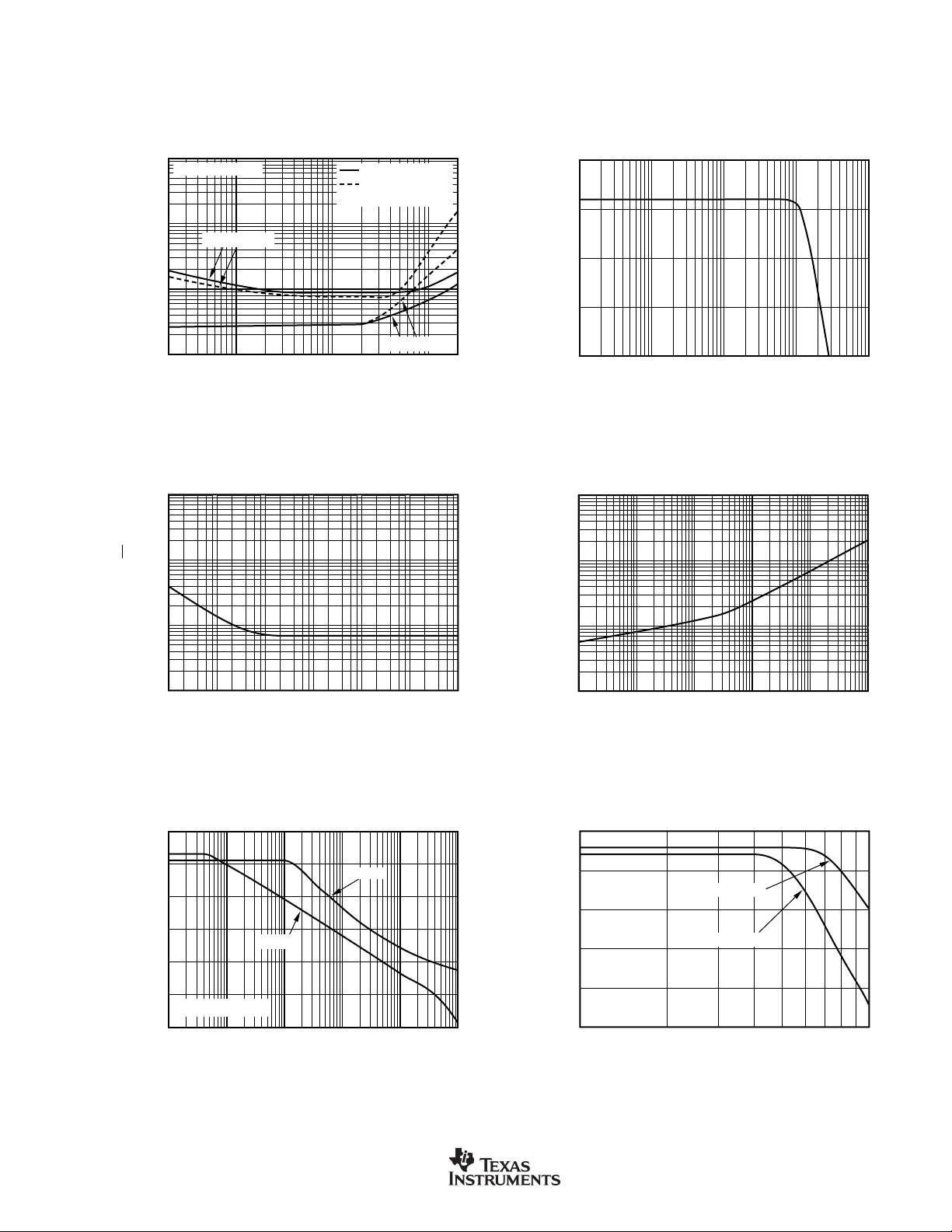
TYPICAL PERFORMANCE CURVES (Cont.)
At TA = +25°C, VS = ±18V, RL = 600Ω differential connected between +VO and –VO, unless otherwise noted.
HARMONIC DISTORTION PRODUCTS
0.01
Differential Mode
0.001
2nd Harmonic
0.0001
Amplitude (% of Fundamental)
0.00001
20 100 1k 20k10k
OUTPUT VOLTAGE NOISE SPECTRAL DENSITY
10k
1k
vs FREQUENCY
Frequency (Hz)
vs FREQUENCY
No Cable, RL = ∞
500 ft Cable,
R
= 600Ω
L
3rd Harmonic
10
5
0
Voltage Gain (dB)
–5
–10
1k 10k 100k 10M1M
100
10
GAIN vs FREQUENCY
Frequency (Hz)
OUTPUT VOLTAGE NOISE
vs NOISE BANDWIDTH
100
Voltage Noise (nV/√Hz)
10
1 10 100 1k 10k 100k 1M
Frequency (Hz)
120
100
80
60
40
20
Power Supply Rejection (dB)
POWER SUPPLY REJECTION vs FREQUENCY
+PSRR
–PSRR
VS = ±4.5V to ±18V
0
10 100 1k 1M100k10k
Frequency (Hz)
1
Voltage Noise (µVrms)
0.1
1 10 100 1k 10k 100k
Frequency (Hz)
MAXIMUM OUTPUT VOLTAGE SWING
20
16
12
8
4
R
Output Voltage Swing (Vrms)
= 600Ω
L
Diff Mode
0
10k 20k 100k80k50k
vs FREQUENCY
0.1% Distortion
0.01% Distortion
Frequency (Hz)
DRV134, DRV135
SBOS094A
www.ti.com
5
Page 6
TYPICAL PERFORMANCE CURVES (Cont.)
At TA = +25°C, VS = ±18V, RL = 600Ω differential connected between +VO and –VO, unless otherwise noted.
THD+N ≤ 0.1%
OUTPUT VOLTAGE SWING
20
THD+N ≤ 0.1%
16
12
8
4
Differential Output Voltage (Vrms)
0
±4 ±6
±5.6
±5.4
±5.2
±5
±4.8
Quiescent Current (mA)
vs SUPPLY VOLTAGE
±8 ±10 ±12 ±14 ±16 ±18
Supply Voltage (V)
QUIESCENT CURRENT
vs SUPPLY VOLTAGE
T = –55°C
T = +25°C
T = +125°C
OUTPUT VOLTAGE SWING
18
16
14
12
10
8
–8
–10
–12
–14
Output Voltage Swing (V)
–16
–18
0 ±20 ±40 ±60 ±80 ±100
±120
±100
±80
±60
±40
Short-Circuit Current (mA)
SHORT-CIRCUIT CURRENT vs TEMPERATURE
vs OUTPUT CURRENT
+125°C
+125°C
Output Current (mA)
+25°C –55°C
+I
SC
–I
SC
+25°C
–55°C
±4.6
±4 ±18±16±14±12±10±8±6
45
40
35
30
25
20
15
Percent of Units (%)
10
5
0
–9–8–7–6–5–4–3–2–1
–10
Supply Voltage (V)
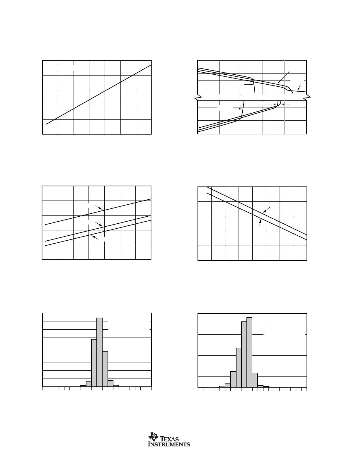
DIFFERENTIAL OFFSET VOLTAGE
PRODUCTION DISTRIBUTION
Typical production
distribution of packaged
units. All package types
included.
012345678
Differential Offset Voltage (mV)
±20
–75 –50 –25 0 25 50 75 125100
Temperature (°C)
COMMON-MODE OFFSET VOLTAGE
35
30
25
20
15
10
Percent of Units (%)
5
9
10
0
–250
–225
PRODUCTION DISTRIBUTION
0
–150
–125
–100
–75
–200
–175
Common-Mode Offset Voltage (mV)
255075
–50
–25
Typical production
distribution of packaged
units. All package types
included.
100
125
150
175
200
225
250
6
www.ti.com
DRV134, DRV135
SBOS094A
Page 7

TYPICAL PERFORMANCE CURVES (Cont.)
At TA = +25°C, VS = ±18V, RL = 600Ω differential connected between +VO and –VO, unless otherwise noted.
50mV/div
SMALL-SIGNAL STEP RESPONSE
= 100pF
C
L
2µs/div
LARGE-SIGNAL STEP RESPONSE
= 100pF
C
L
50mV/div
SMALL-SIGNAL STEP RESPONSE
= 1000pF
C
L
2µs/div
LARGE-SIGNAL STEP RESPONSE
= 1000pF
C
L
5V/div
2µs/div
5V/div
2µs/div
SMALL-SIGNAL OVERSHOOT
vs LOAD CAPACITANCE
40
100mV Step
30
20
Overshoot (%)
10
0
10 1k100 10k
Load Capacitance (pF)
DRV134, DRV135
SBOS094A
www.ti.com
7
Page 8

APPLICATIONS INFORMATION
The DRV134 (and DRV135 in SO-8 package) converts a
single-ended, ground-referenced input to a floating differential output with +6dB gain (G = 2). Figure 1 shows the
basic connections required for operation. Decoupling capacitors placed close to the device pins are strongly recommended in applications with noisy or high impedance power
supplies.
The DRV134 consists of an input inverter driving a crosscoupled differential output stage with 50Ω series output
resistors. Characterized by low differential-mode output
impedance (50Ω) and high common-mode output impedance (1.6kΩ), the DRV134 is ideal for audio applications.
Normally, +VO is connected to +Sense, –VO is connected to
–Sense, and the outputs are taken from these junctions as
shown in Figure 1. For applications with large dc cable
offset errors, a 10µF electrolytic nonpolarized blocking
capacitor at each sense pin is recommended as shown in
Figure 2.
1µF
4
V
IN
(6)
Gnd
SOL-16 pin numbers in parentheses.
3
(5)
FIGURE 1. Basic Connections.
V–
5 (11)
DRV134
DRV135
A1
All resistors 30kΩ unless otherwise indicated.
A2
A3
10kΩ
10kΩ
V+
50Ω
50Ω
1µF
(12)6
8
(14)
7
(13)
2
(4)
1
(3)
+Sense
–Sense
+V
G = +6dB
–V
O
O
DRIVER
DRV134
DRV135
A2
10kΩ
A3
Gnd
4
V
IN
3
All resistors 30kΩ unless otherwise indicated.
Pin numbers shown for DIP and SO-8 versions.
NOTE: (1) Optional 10µF electrolytic (nonpolarized) capacitors reduce common-mode offset errors.
A1
FIGURE 2. Complete Audio Driver/Receiver Circuit.
8
10kΩ
50Ω
8
10µF
7
10µF
2
50Ω
1
www.ti.com
RECEIVER
–V
(1)
(1)
BALANCED
+V
O
CABLE PAIR
–V
O
O
2
3
+V
O
INA134, INA137
INA134 (G = 1): VO = 2V
INA137 (G = 1/2): VO = V
5
6
V
O
1
IN
IN
DRV134, DRV135
SBOS094A
Page 9

Excellent internal design and layout techniques provide low
( )
V
OD
V
CM
600Ω
V
CM
= 10Vp-p
300Ω
(1)
300Ω
(1)
OCMR = –20 Log at f = 1kHz, VOD = (+VO) – (–VO)
NOTE: (1) Matched to 0.1%.
V
IN
Gnd
+V
O
V
OD
–V
O
DRV134
1µF
+18V
6
8
1
7
2
1µF
–18V
5
4
3
signal distortion, high output level (+27dBu), and a low
noise floor (–98dBu). Laser trimming of thin film resistors
assures excellent output common-mode rejection (OCMR)
and signal balance ratio (SBR). In addition, low dc voltage
offset reduces errors and minimizes load currents.
For best system performance, it is recommended that a high
input-impedance difference amplifier be used as the receiver. Used with the INA134 (G = 0dB) or the INA137 (G
= ±6dB) differential line receivers, the DRV134 forms a
complete solution for driving and receiving audio signals,
replacing input and output coupling transformers commonly
used in professional audio systems (Figure 2). When used
with the INA137 (G = –6dB) overall system gain is unity.
AUDIO PERFORMANCE
The DRV134 was designed for enhanced ac performance.
Very low distortion, low noise, and wide bandwidth provide
superior performance in high quality audio applications.
Laser-trimmed matched resistors provide optimum output
common-mode rejection (typically 68dB), especially when
compared to circuits implemented with op amps and discrete
precision resistors. In addition, high slew rate (15V/µs) and
fast settling time (2.5µs to 0.01%) ensure excellent dynamic
response.
The DRV134 has excellent distortion characteristics. As
shown in the distortion data provided in the typical performance curves, THD+Noise is below 0.003% throughout the
audio frequency range under various output conditions. Both
differential and single-ended modes of operation are shown.
In addition, the optional 10µF blocking capacitors used to
minimize V
errors have virtually no effect on perfor-
OCM
mance. Measurements were taken with an Audio Precision
System One (with the internal 80kHz noise filter) using the
THD test circuit shown in Figure 3.
Up to approximately 10kHz, distortion is below the measurement limit of commonly used test equipment. Furthermore, distortion remains relatively constant over the wide
output voltage swing range (approximately 2.5V from the
positive supply and 1.5V from the negative supply). A
special output stage topology yields a design with minimum
distortion variation from lot-to-lot and unit-to-unit. Furthermore, the small and large signal transient response curves
demonstrate the DRV134’s stability under load.
OUTPUT COMMON-MODE REJECTION
Output common-mode rejection (OCMR) is defined as the
change in differential output voltage due to a change in
output common-mode voltage. When measuring OCMR,
VIN is grounded and a common-mode voltage, VCM, is
applied to the output as shown in Figure 4. Ideally no
differential mode signal (VOD) should appear. However, a
small mode-conversion effect causes an error signal whose
magnitude is quantified by OCMR.
FIGURE 3. Distortion Test Circuit.
DRV134, DRV135
V
SBOS094A
IN
4
DRV134
3
NOTE: Cable loads, where indicated, are Belden 9452 cable.
+18V
–18V
FIGURE 4. Output Common-Mode Rejection Test Circuit.
+18V
1µF
+V
O
6
7
8
1
2
5
–V
O
1µF
R
R
1
2
www.ti.com
Test Point
or
R
L
–In
2
INA137
+In
3
–18V
1µF
7
5
6
1
4
1µF
V
OUT
9
Page 10

SIGNAL BALANCE RATIO
Signal balance ratio (SBR) measures the symmetry of the
output signals under loaded conditions. To measure SBR an
input signal is applied and the outputs are summed as shown
in Figure 5. V
should be zero since each output ideally
OUT
is exactly equal and opposite. However, an error signal
results from any imbalance in the outputs. This error is
quantified by SBR. The impedances of the DRV134’s out
put stages are closely matched by laser trimming to minimize SBR errors. In an application, SBR also depends on the
balance of the load network.
+18V
For best rejection of line noise and hum differential mode
operation is recommended. However, single-ended performance is adequate for many applications. In general singleended performance is comparable to differential mode (see
THD+N typical performance curves), but the commonmode and noise rejection inherent in balanced-pair systems
is lost.
CABLE
The DRV134 is capable of driving large signals into 600Ω
loads over long cables. Low impedance shielded audio
cables such as the standard Belden 8451 or 9452 (or similar)
are recommended, especially in applications where long
cable lengths are required.
1µF
(1)
VIN = 10Vp-p
Gnd
NOTE: (1) Matched to 0.1%.
4
3
6
DRV134
5
–18V
+V
7
8
1
2
–V
300Ω
O
(1)
300Ω
O
1µF
SBR = –20 Log at f = 1kHz
( )
V
OUT
V
600Ω
IN
V
OUT
FIGURE 5. Signal Balance Ratio Test Circuit.
SINGLE-ENDED OPERATION
The DRV134 can be operated in single-ended mode without
degrading output drive capability. Single-ended operation
requires that the unused side of the output pair be grounded
(both the V
and Sense pins) to a low impedance return path.
O
Gain remains +6dB. Grounding the negative outputs as
shown in Figure 6 results in a noninverted output signal
(G = +2) while grounding the positive outputs gives an
inverted output signal (G = –2).
V+
= 2V
V
OUT
IN
V
IN
4
3
6
DRV134
5
V–
7
8
1
2
600Ω
G = +6dB
THERMAL PERFORMANCE
The DRV134 and DRV135 have robust output drive capability and excellent performance over temperature. In most
applications there is no significant difference between the
DIP, SOL-16, and SO-8 packages. However, for applications with extreme temperature and load conditions, the
SOL-16 (DRV134UA) or DIP (DRV134PA) packages are
recommended. Under these conditions, such as loads greater
than 600Ω or very long cables, performance may be degraded in the SO-8 (DRV135UA) package.
LAYOUT CONSIDERATIONS
A driver/receiver balanced-pair (such as the DRV134 and
INA137) rejects the voltage differences between the grounds
at each end of the cable, which can be caused by ground
currents, supply variations, etc. In addition to proper bypassing, the suggestions below should be followed to achieve
optimal OCMR and noise rejection.
• The DRV134 input should be driven by a low impedance
source such as an op amp or buffer.
• As is the case for any single-ended system, the source’s
common should be connected as close as possible to the
DRV134’s ground. Any ground offset errors in the source
will degrade system performance.
• Symmetry on the outputs should be maintained.
• Shielded twisted-pair cable is recommended for all applications. Physical balance in signal wiring should be maintained. Capacitive differences due to varying wire lengths
may result in unequal noise pickup between the pair and
degrade OCMR. Follow industry practices for proper system grounding of the cables.
FIGURE 6. Typical Single-Ended Application.
10
www.ti.com
DRV134, DRV135
SBOS094A
Page 11

PACKAGE OPTION ADDENDUM
www.ti.com
22-Oct-2007
PACKAGING INFORMATION
Orderable Device Status
(1)
Package
Type
Package
Drawing
Pins Package
Qty
Eco Plan
DRV134PA ACTIVE PDIP P 8 50 Green (RoHS &
no Sb/Br)
DRV134PAG4 ACTIVE PDIP P 8 50 Green (RoHS &
no Sb/Br)
DRV134UA ACTIVE SOIC DW 16 48 Green (RoHS &
no Sb/Br)
DRV134UA/1K ACTIVE SOIC DW 16 1000 Green (RoHS &
no Sb/Br)
DRV134UA/1KE4 ACTIVE SOIC DW 16 1000 Green (RoHS &
no Sb/Br)
DRV134UAE4 ACTIVE SOIC DW 16 48 Green (RoHS &
no Sb/Br)
DRV135UA ACTIVE SOIC D 8 100 Green (RoHS &
no Sb/Br)
DRV135UA/2K5 ACTIVE SOIC D 8 2500 Green (RoHS &
no Sb/Br)
DRV135UA/2K5E4 ACTIVE SOIC D 8 2500 Green (RoHS &
no Sb/Br)
DRV135UAG4 ACTIVE SOIC D 8 100 Green (RoHS &
no Sb/Br)
(1)
The marketing status values are defined as follows:
ACTIVE: Product device recommended for new designs.
LIFEBUY: TI has announced that the device will be discontinued, and a lifetime-buy period is in effect.
NRND: Not recommended for new designs. Device is in production to support existing customers, but TI does not recommend using this part in
a new design.
PREVIEW: Device has been announced but is not in production. Samples may or may not be available.
OBSOLETE: TI has discontinued the production of the device.
(2)
Lead/Ball Finish MSL Peak Temp
CU NIPDAU N / A for Pkg Type
CU NIPDAU N / A for Pkg Type
CU NIPDAU Level-3-260C-168 HR
CU NIPDAU Level-3-260C-168 HR
CU NIPDAU Level-3-260C-168 HR
CU NIPDAU Level-3-260C-168 HR
CU NIPDAU Level-3-260C-168 HR
CU NIPDAU Level-3-260C-168 HR
CU NIPDAU Level-3-260C-168 HR
CU NIPDAU Level-3-260C-168 HR
(3)
(2)
Eco Plan - The planned eco-friendly classification: Pb-Free (RoHS), Pb-Free (RoHS Exempt), or Green (RoHS & no Sb/Br) - please check
http://www.ti.com/productcontent for the latest availability information and additional product content details.
TBD: The Pb-Free/Green conversion plan has not been defined.
Pb-Free (RoHS): TI's terms "Lead-Free" or "Pb-Free" mean semiconductor products that are compatible with the current RoHS requirements
for all 6 substances, including the requirement that lead not exceed 0.1% by weight in homogeneous materials. Where designed to be soldered
at high temperatures, TI Pb-Free products are suitable for use in specified lead-free processes.
Pb-Free (RoHS Exempt): This component has a RoHS exemption for either 1) lead-based flip-chip solder bumps used between the die and
package, or 2) lead-based die adhesive used between the die and leadframe. The component is otherwise considered Pb-Free (RoHS
compatible) as defined above.
Green (RoHS & no Sb/Br): TI defines "Green" to mean Pb-Free (RoHS compatible), and free of Bromine (Br) and Antimony (Sb) based flame
retardants (Br or Sb do not exceed 0.1% by weight in homogeneous material)
(3)
MSL, Peak Temp. -- The Moisture Sensitivity Level rating according to the JEDEC industry standard classifications, and peak solder
temperature.
Important Information and Disclaimer:The information provided on this page represents TI's knowledge and belief as of the date that it is
provided. TI bases its knowledge and belief on information provided by third parties, and makes no representation or warranty as to the
accuracy of such information. Efforts are underway to better integrate information from third parties. TI has taken and continues to take
reasonable steps to provide representative and accurate information but may not have conducted destructive testing or chemical analysis on
incoming materials and chemicals. TI and TI suppliers consider certain information to be proprietary, and thus CAS numbers and other limited
information may not be available for release.
In no event shall TI's liability arising out of such information exceed the total purchase price of the TI part(s) at issue in this document sold by TI
to Customer on an annual basis.
Addendum-Page 1
Page 12

PACKAGE MATERIALS INFORMATION
www.ti.com
TAPE AND REEL INFORMATION
11-Mar-2008
*All dimensions are nominal
Device Package
DRV134UA/1K SOIC DW 16 1000 330.0 16.4 10.85 10.8 2.7 12.0 16.0 Q1
DRV135UA/2K5 SOIC D 8 2500 330.0 12.4 6.4 5.2 2.1 8.0 12.0 Q1
Type
Package
Drawing
Pins SPQ Reel
Diameter
(mm)
Reel
Width
W1 (mm)
A0 (mm) B0 (mm) K0 (mm) P1
(mm)W(mm)
Pin1
Quadrant
Pack Materials-Page 1
Page 13

PACKAGE MATERIALS INFORMATION
www.ti.com
11-Mar-2008
*All dimensions are nominal
Device Package Type Package Drawing Pins SPQ Length (mm) Width (mm) Height (mm)
DRV134UA/1K SOIC DW 16 1000 346.0 346.0 33.0
DRV135UA/2K5 SOIC D 8 2500 346.0 346.0 29.0
Pack Materials-Page 2
Page 14

Page 15

MECHANICAL DATA
MPDI001A – JANUARY 1995 – REVISED JUNE 1999
P (R-PDIP-T8) PLASTIC DUAL-IN-LINE
0.400 (10,60)
0.355 (9,02)
8
5
0.260 (6,60)
0.240 (6,10)
1
0.021 (0,53)
0.015 (0,38)
NOTES: A. All linear dimensions are in inches (millimeters).
B. This drawing is subject to change without notice.
C. Falls within JEDEC MS-001
4
0.070 (1,78) MAX
0.020 (0,51) MIN
0.200 (5,08) MAX
0.125 (3,18) MIN
0.100 (2,54)
0.010 (0,25)
Seating Plane
M
0.325 (8,26)
0.300 (7,62)
0.015 (0,38)
Gage Plane
0.010 (0,25) NOM
0.430 (10,92)
MAX
4040082/D 05/98
For the latest package information, go to http://www.ti.com/sc/docs/package/pkg_info.htm
POST OFFICE BOX 655303 • DALLAS, TEXAS 75265
Page 16

Page 17

IMPORTANT NOTICE
Texas Instruments Incorporated and its subsidiaries (TI) reserve the right to make corrections, modifications, enhancements, improvements,
and other changes to its products and services at any time and to discontinue any product or service without notice. Customers should
obtain the latest relevant information before placing orders and should verify that such information is current and complete. All products are
sold subject to TI’s terms and conditions of sale supplied at the time of order acknowledgment.
TI warrants performance of its hardware products to the specifications applicable at the time of sale in accordance with TI’s standard
warranty. Testing and other quality control techniques are used to the extent TI deems necessary to support this warranty. Except where
mandated by government requirements, testing of all parameters of each product is not necessarily performed.
TI assumes no liability for applications assistance or customer product design. Customers are responsible for their products and
applications using TI components. To minimize the risks associated with customer products and applications, customers should provide
adequate design and operating safeguards.
TI does not warrant or represent that any license, either express or implied, is granted under any TI patent right, copyright, mask work right,
or other TI intellectual property right relating to any combination, machine, or process in which TI products or services are used. Information
published by TI regarding third-party products or services does not constitute a license from TI to use such products or services or a
warranty or endorsement thereof. Use of such information may require a license from a third party under the patents or other intellectual
property of the third party, or a license from TI under the patents or other intellectual property of TI.
Reproduction of TI information in TI data books or data sheets is permissible only if reproduction is without alteration and is accompanied
by all associated warranties, conditions, limitations, and notices. Reproduction of this information with alteration is an unfair and deceptive
business practice. TI is not responsible or liable for such altered documentation. Information of third parties may be subject to additional
restrictions.
Resale of TI products or services with statements different from or beyond the parameters stated by TI for that product or service voids all
express and any implied warranties for the associated TI product or service and is an unfair and deceptive business practice. TI is not
responsible or liable for any such statements.
TI products are not authorized for use in safety-critical applications (such as life support) where a failure of the TI product would reasonably
be expected to cause severe personal injury or death, unless officers of the parties have executed an agreement specifically governing
such use. Buyers represent that they have all necessary expertise in the safety and regulatory ramifications of their applications, and
acknowledge and agree that they are solely responsible for all legal, regulatory and safety-related requirements concerning their products
and any use of TI products in such safety-critical applications, notwithstanding any applications-related information or support that may be
provided by TI. Further, Buyers must fully indemnify TI and its representatives against any damages arising out of the use of TI products in
such safety-critical applications.
TI products are neither designed nor intended for use in military/aerospace applications or environments unless the TI products are
specifically designated by TI as military-grade or "enhanced plastic." Only products designated by TI as military-grade meet military
specifications. Buyers acknowledge and agree that any such use of TI products which TI has not designated as military-grade is solely at
the Buyer's risk, and that they are solely responsible for compliance with all legal and regulatory requirements in connection with such use.
TI products are neither designed nor intended for use in automotive applications or environments unless the specific TI products are
designated by TI as compliant with ISO/TS 16949 requirements. Buyers acknowledge and agree that, if they use any non-designated
products in automotive applications, TI will not be responsible for any failure to meet such requirements.
Following are URLs where you can obtain information on other Texas Instruments products and application solutions:
Products Applications
Amplifiers amplifier.ti.com Audio www.ti.com/audio
Data Converters dataconverter.ti.com Automotive www.ti.com/automotive
DSP dsp.ti.com Broadband www.ti.com/broadband
Clocks and Timers www.ti.com/clocks Digital Control www.ti.com/digitalcontrol
Interface interface.ti.com Medical www.ti.com/medical
Logic logic.ti.com Military www.ti.com/military
Power Mgmt power.ti.com Optical Networking www.ti.com/opticalnetwork
Microcontrollers microcontroller.ti.com Security www.ti.com/security
RFID www.ti-rfid.com Telephony www.ti.com/telephony
RF/IF and ZigBee® Solutions www.ti.com/lprf Video & Imaging www.ti.com/video
Mailing Address: Texas Instruments, Post Office Box 655303, Dallas, Texas 75265
Copyright © 2008, Texas Instruments Incorporated
Wireless www.ti.com/wireless
 Loading...