

Page 1
查询DAC1221供应商
®
For most current data sheet and other product
information, visit www.burr-brown.com
16-Bit Low Power
DIGITAL-TO-ANALOG CONVERTER
FEATURES
● 16-BIT MONOTONICITY GUARANTEED
OVER –40°C TO +85°C
● LOW POWER: 1.2mW
● VOLTAGE OUTPUT
● SETTLING TIME: 2ms to 0.012%
● MAX LINEARITY ERROR: 30ppm
● ON-CHIP CALIBRATION
DAC1221
DAC1221
APPLICATIONS
● PROCESS CONTROL
● ATE PIN ELECTRONICS
● CLOSED-LOOP SERVO-CONTROL
● SMART TRANSMITTERS
● PORTABLE INSTRUMENTS
● VCO CONTROL
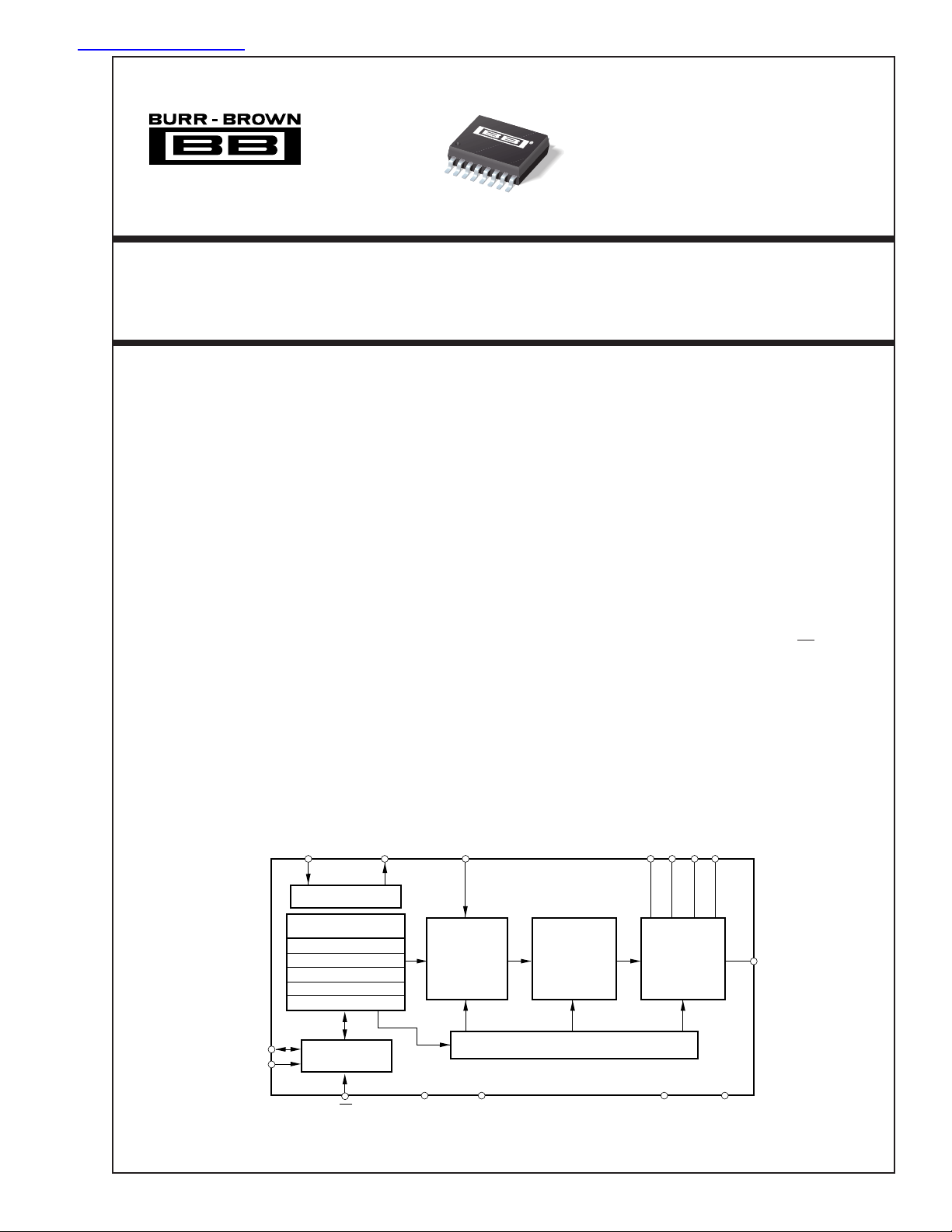
DESCRIPTION
The DAC1221 is a Digital-to-Analog (D/A) converter
offering 16-bit monotonic performance over the specified temperature range. It utilizes delta-sigma technology to achieve inherently linear performance in a
small package at very low power. The output range is
two times the external reference voltage. On-chip
calibration circuitry dramatically reduces offset and
gain errors.
X
IN
Clock Generator
Microcontroller
Instruction Register
Command Register
Data Register
Offset Register
Full-Scale Register
X
OUT
V
REF
Second-Order
∆∑
Modulator
The DAC1221 features a synchronous serial interface.
In single converter applications, the serial interface can
be accomplished with just two wires, allowing lowcost isolation. For multiple converters, a CS signal
allows for selection of the appropriate D/A converter.
The DAC1221 has been designed for closed-loop
control applications in the industrial process control
market, and high resolution applications in the test and
measurement market. It is also ideal for remote applications, battery-powered instruments, and isolated systems.
The DAC1221 is available in a SSOP-16 package.
C2AC2BC
First-Order
Switched
Capacitor Filter
C
1
Second-Order
Continuous
Time Post Filter
3
V
OUT
SDIO
SCLK
International Airport Industrial Park • Mailing Address: PO Box 11400, Tucson, AZ 85734 • Street Address: 6730 S. Tucson Blvd., Tucson, AZ 85706 • Tel: (520) 746-1111
Twx: 910-952-1111 • Internet: http://www.burr-brown.com/ • Cable: BBRCORP • Telex: 066-6491 • FAX: (520) 889-1510 • Immediate Product Info: (800) 548-6132
© 1999 Burr-Brown Corporation PDS-1519B Printed in U.S.A. May, 2000
Serial
Interface
CS DV
DGND AV
DD
Modulator Control
1
AGND
DD
DAC1221
®
Page 2
SPECIFICATIONS
All specifications T
PARAMETER CONDITIONS MIN TYP MAX UNITS
ACCURACY
Monotonicity 16 Bits
Linearity Error
Offset Error
Offset Error Drift
Midscale Error
Midscale Error Drift
Gain Error
Gain Error Drift
Power-Supply Rejection Ratio at DC, dB = –20log(∆V
to T
MIN
, AVDD = DVDD = +3V, f
MAX
= 2.5MHz, V
XIN
= +1.25V, C1 = 2.2nF, C2 = 150pF, C3 = 6.8nF, unless otherwise noted.
REF
DAC1221E
(1)
(2)
(3)
(2)
(3)
(2)
(3)
V
= 20mV, CALPIN = 1
OUT
V
= V
OUT
, CALPIN = 1
REF
CALPIN = 1
(6)
(6)
(6)
50 µV/°C
±20 µV
50 µV/°C
3 ppm/°C
/∆VDD)57dB
OUT
±30 ppm of FSR
±190 µV
0.015 %
ANALOG OUTPUT
Output Voltage
Output Current
(4)
(1)
0 2 • V
±0.25 mA
REF
Capacitive Load 500 pF
Short-Circuit Current ±10 mA
Short-Circuit Duration GND or V
DYNAMIC PERFORMANCE
Settling Time
(1,5)
To ±0.012% 1.8 2 ms
DD
Indefinite
Output-Noise Voltage 1Hz to 2kHz 45 µVrms
REFERENCE INPUT
Input Voltage 1.125 1.25 1.375 V
Input Impedance 1MΩ
DIGITAL INPUT/OUTPUT
Logic Family TTL-Compatible CMOS
Logic Levels (all except X
V
IH
V
IL
V
OH
V
OL
Input-Leakage Current ±10 µA
Frequency Range (f
X
IN
Data Format User Programmable Offset Two’s Complement
)
IN
2.0 DVDD + 0.3 V
–0.3 0.8 V
IOH = –0.8mA 2.4 V
IOL = 1.6mA 0.4 V
) 1.0 2.5 MHz
XIN
or Straight Binary
POWER SUPPLY REQUIREMENTS
Power-Supply Voltage 2.7 3.3 V
Supply Current
Analog Current 320 µA
Digital Current 70 µA
Power Dissipation Normal Mode 1.2 1.6 mW
Sleep Mode 0.25 mW
TEMPERATURE RANGE
Specified Performance –40 +85 °C
NOTES: (1) Valid from AGND + 20mV to 2 • V
low-pass filter with 2kHz corner frequency. (6) See Command Register for description of CALPIN.
. (2) Applies after calibration. (3) Recalibration can remove these errors. (4) Ideal output voltage. (5) Using external
REF
V
®
DAC1221
2
Page 3
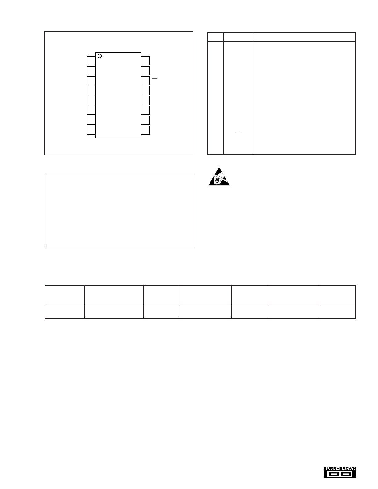
PIN CONFIGURATION
PIN DESCRIPTIONS
Top View SSOP
DV
1
DD
X
2
OUT
X
3
IN
4
DGND
AV
DNC
C
DD
C
3
2B
DAC1221E
5
6
7
8
ABSOLUTE MAXIMUM RATINGS
AV
to DVDD................................................................................... ±0.3V
DD
to AGND ........................................................................ –0.3V to 4V
AV
DD
to DGND ....................................................................... –0.3V to 4V
DV
DD
AGND to DGND ............................................................................... ±0.3V
Voltage to AGND .......................................................... 1.0V to 1.5V
V
REF
Digital Input Voltage to DGND .............................. –0.3V to DV
Digital Output Voltage to DGND ........................... –0.3V to DV
Package Power Dissipation ............................................. (T
Maximum Junction Temperature (T
Thermal Resistance,
SSOP-16............................................................................... 200°C/W
θ
JA
) ..................................... +150°C
JMAX
SCLK
16
SDIO
15
CS
14
AGND
13
V
12
REF
11
V
OUT
10
C
2A
9
C
1
(1)
+ 0.3V
DD
+ 0.3V
DD
– TA)/
JMAX
θ
JA
Lead Temperature (soldering, 10s) ............................................... +300°C
NOTE: (1) Stresses above those listed under “Absolute Maximum Ratings”
may cause permanent damage to the device. Exposure to absolute maximum
conditions for extended periods may affect device reliability.
PIN NAME DESCRIPTION
1DV
2X
3X
OUT
IN
Digital Supply, +3V nominal
DD
Digital, System Clock Output
Digital, System Clock Input
4 DGND Digital Ground
5AV
Analog Supply, +3V nominal
DD
6 DNC Do Not Connect
7C
8C
2B
9C
10 C
11 V
12 V
2A
OUT
REF
Analog, Filter Capacitor
3
Analog, Filter Capacitor
Analog, Filter Capacitor
1
Analog, Filter Capacitor
Analog Output Voltage
Analog, Reference Input
13 AGND Analog Ground
14 CS Digital, Chip Select Input
15 SDIO Digital, Serial Data Input/Output
16 SCLK Digital, Clock Input for Serial Data Transfer
ELECTROSTATIC
DISCHARGE SENSITIVITY
This integrated circuit can be damaged by ESD. Burr-Brown
recommends that all integrated circuits be handled with
appropriate precautions. Failure to observe proper handling
and installation procedures can cause damage.
ESD damage can range from subtle performance degradation
to complete device failure. Precision integrated circuits may
be more susceptible to damage because very small parametric
changes could cause the device not to meet its published
specifications.
PACKAGE/ORDERING INFORMATION
PACKAGE SPECIFIED
PRODUCT PACKAGE NUMBER RANGE MARKING NUMBER
DRAWING TEMPERATURE PACKAGE ORDERING TRANSPORT
DAC1221E SSOP-16 322 –40°C to +85°C DAC1221E DAC1221E Rails
" " " " " DAC1221E/2K5 Tape and Reel
NOTE: (1) Models with a slash (/) are available only in Tape and Reel in the quantities indicated (e.g., /2K5 indicates 2500 devices per reel). Ordering 2500 pieces
of “DAC1221E/2K5” will get a single 2500-piece Tape and Reel.
The information provided herein is believed to be reliable; however, BURR-BROWN assumes no responsibility for inaccuracies or omissions. BURR-BROWN assumes
no responsibility for the use of this information, and all use of such information shall be entirely at the user’s own risk. Prices and specifications are subject to change
without notice. No patent rights or licenses to any of the circuits described herein are implied or granted to any third party. BURR-BROWN does not authorize or warrant
any BURR-BROWN product for use in life support devices and/or systems.
(1)
MEDIA
®
3
DAC1221
Page 4
TYPICAL PERFORMANCE CURVES
FULL SCALE OUTPUT SWING
Time (ms)
01234
Output (V)
3.0
2.5
2.0
1.5
1.0
0.5
0
At TA = +25°C, AVDD = DVDD = +3.0V, f
POWER SUPPLY REJECTION RATIO vs FREQUENCY
70
60
50
40
30
PSRR (dB)
20
10
0
10 100 1000 10000 100000
Frequency (Hz)
SETTLING TIME: 20mV to FS
300
0
= 2.5MHz, V
XIN
= 1.25V, C1 = 2.2nF, C2 = 150pF and C3 = 6.8nF.
REF
1500
1200
SETTLING TIME: FS to 20mV
–300
–600
–900
∆ Around FS (µV)
–1200
–1500
0246810
Time (ms)
10000
1000
100
Noise (nv/√Hz)
10
1
OUTPUT NOISE VOLTAGE vs FREQUENCY
10 100 1000 10000 10000
Frequency (Hz)
900
600
300
∆ Around 20mV (µV)
0
–300
0246810
Time (ms)
4
2
0
–2
Offset (mV)
–4
–6
OFFSET vs TEMPERATURE
(can be corrected with calibration)
–25 25 75–50 0 50 100
Temperature (°C)
®
DAC1221
4
Page 5
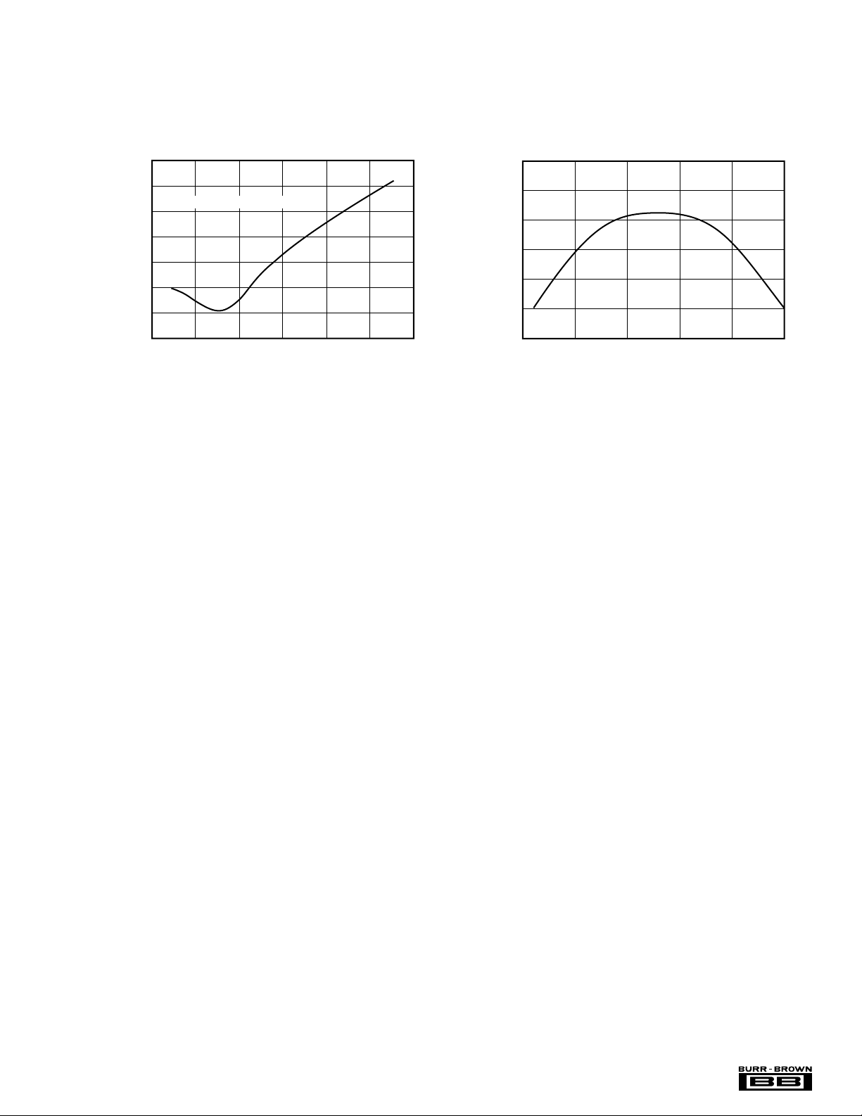
LINEARITY ERROR vs CODE
16-Bit Input Code Normalized
0
0.2 0.4 0.6 0.8 1
Linearity Error (ppm of FSR)
25
20
15
10
5
0
–5
TYPICAL PERFORMANCE CURVES
At TA = +25°C, AVDD = DVDD = +3.0V, f
0.020
0.015
0.010
0.005
0.000
Gain Error (%)
–0.005
–0.010
–0.015
–50 –25
GAIN ERROR vs TEMPERATURE
(can be corrected with calibration)
0507525 100
Temperature (°C)
= 2.5MHz, V
XIN
= 1.25V, C1 = 2.2nF, C2 = 150pF and C3 = 6.8nF.
REF
®
5
DAC1221
Page 6

THEORY OF OPERATION
V
REF
C
2A
C
1
C
3
C
2B
12
11
10
9
7
8
DAC1221
C
3
6.8nF
C
1
2.2nF
C
2
150pF
NOTE: C1 and C2 should be NPO type capacitors.
ANALOG OPERATION
The DAC1221 is a precision, high dynamic range, selfcalibrating, 16-bit, delta-sigma digital-to-analog converter.
It contains a second-order delta-sigma modulator, a firstorder switched-capacitor filter, a second-order continuoustime post filter, a microcontroller including the Instruction,
Command and Calibration registers, a serial interface, and a
clock generator circuit.
The design topology provides low system noise and good
power-supply rejection. The modulator frequency of the
delta-sigma D/A converter is controlled by the system clock.
The DAC1221 also includes complete onboard calibration
that can correct for internal offset and gain errors.
The calibration registers are fully readable and writable.
This feature allows for system calibration. The various
settings, modes, and registers of the DAC1221 are read or
written via a synchronous serial interface. This interface
operates as an externally clocked interface.
DEFINITION OF TERMS
Differential Nonlinearity Error—The differential
nonlinearity error is the difference between an actual step
width and the ideal value of 1 LSB. If the step width is
exactly 1 LSB, the differential nonlinearity error is zero.
A differential nonlinearity specification of less than 1 LSB
guarantees monotonicity.
Drift—The drift is the change in a parameter over temperature.
Full-Scale Range (FSR)—This is the magnitude of the
typical analog output voltage range which is 2 • V
For example, when the converter is configured with a 1.25V
reference, the full-scale range is 2.5V.
Gain Error—This error represents the difference in the
slope between the actual and ideal transfer functions.
Linearity Error—The linearity error is the deviation of the
actual transfer function from an ideal straight line between
the data end points.
Least Significant Bit (LSB) Weight—This is the ideal
change in voltage that the analog output will change with a
change in the digital input code of 1 LSB.
Monotonicity—Monotonicity assures that the analog output
will increase or stay the same for increasing digital input
codes.
Offset Error—The offset error is the difference between the
expected and actual output, when the output is zero. The
value is calculated from measurements made when
V
= 20mV.
OUT
Settling Time—The settling time is the time it takes the
output to settle to its new value after the digital code has
been changed.
f
—The frequency of the crystal oscillator or CMOS-
XIN
compatible input signal at the XIN input of the DAC1221.
REF
The system clock is divided down to provide the sample
clock for the modulator. The sample clock is used by the
modulator to convert the multi-bit digital input into a 1-bit
digital output stream. The use of a 1-bit DAC provides
inherent linearity. The digital output stream is then converted into an analog signal via the 1-bit DAC and then
filtered by the 1st-order switched-capacitor filter.
The output of the switched-capacitor filter feeds into the
continuous time filter. The continuous time filter uses external capacitors, C1 and C2, to adjust the settling time. The
connections for capacitors are shown in Figure 1. C1 connects to V
connected between C3 and V
. C2 connects between the C2 pins. C3 is
REF
, and is used for calibration.
REF
.
FIGURE 1. Capacitor Connections.
CALIBRATION
The DAC1221 offers a self-calibration mode which automatically calibrates the output offset and gain. The calibration is performed once and then normal operation is resumed. In general, calibration is recommended immediately
after power-on and whenever there is a “significant” change
in the operating environment. The amount of change which
should cause re-calibration is dependent on the application.
Where high accuracy is important, re-calibration should be
done on changes in temperature and power supply.
After a calibration has been accomplished, the Offset Calibration Register (OCR) and the Full-Scale Calibration Register (FCR) contain the results of the calibration.
Note that the values in the calibration registers will vary
from configuration to configuration and from part to part.
®
DAC1221
6
Page 7

Self Calibration
A self-calibration is performed after the bits “01” have been
written to the Command Register Operation Mode bits
(MD1 and MD0). This initiates a self-calibration on the next
clock cycle. The offset correction code is determined by a
repeated sequence of auto-zeroing the calibration comparator to the offset reference and then comparing the DAC
output to the offset reference value. The end result is the
averaged, Offset Two’s Complement adjusted, and placed in
the OCR. The gain correction is done in a similar fashion,
except the correction is done against V
to eliminate
REF
common-mode errors. The FCR result represents the gain
code and is not Offset Two’s Complement adjusted.
The calibration function takes between 300ms and 500ms
(for f
= 2.5MHz) to complete. Once calibration is initi-
XIN
ated, further writing of register bits is disabled until calibration completes. The status of calibration can be verified by
reading the status of the Command Register Operation Mode
bits (MD1 and MD0). These bits will return to normal mode
“00” when calibration is complete.
It is recommended that the output be connected during
calibration. The output isolation is controlled by the CALPIN
bit in the CMR register. Setting the CALPIN bit will connect
the output and clearing the bit will disconnect and isolate the
output. Although it is recommended to connect the output
during calibration, the load impedance should be such that
the DAC1221 is not required to sink any current, but is able
to source up to the specified maximum.
Output Mode
The output of the DAC1221 can be synchronously reset.
By setting the CLR bit in the CMR, the data input register
is cleared to zero. This will result in an output of 0V when
DF = 1, or V
when DF = 0.
REF
The settling time is determined by the DISF and ADPT bits
of the command register. The default state of DISF = 0 and
ADPT = 0 enables fast settling, unless the output step is
small (≈ 40mV). However, the DAC1221 can be forced to
always use fast settling if the ADPT bit is set to 1. If DISF
is set to 1, all fast settling is disabled.
The CRST bit of the CMR can be used to reset the offset and
calibration registers. By setting the CRST bit, the contents of
the calibration registers are reset to 0.
REFERENCE INPUT
The reference input voltage of 1.25V can be directly connected to V
REF
pin.
The recommended reference circuit for the DAC1221 is
shown in Figure 2.
DIGITAL OPERATION
SYSTEM CONFIGURATION
The DAC1221 is controlled by 8-bit instruction codes (INSR)
and 16-bit command codes (CMR) via the serial interface,
which is externally clocked.
The DAC1221 Microcontroller (MC) consists of an ALU
and a register bank. The MC has three states: power-on
reset, calibration, and normal operation. In the power-on
reset state, the MC resets all the registers to their default
states. In the calibration state, the MC performs offset and
gain self-calibration. In the normal state, the MC performs
D/A conversions.
The DAC1221 has five internal registers, as shown in Table I.
Two of these, the Instruction Register (INSR) and the
Command Register (CMR), control the operation of the
converter. The Instruction Register utilizes an 8-bit instruction code to control the serial interface to determine whether
the next operation is either a read or a write, to control the
word length, and to select the appropriate register to
read/write. Communication with the DAC1221 is controlled
via the INSR. Under normal operation, the INSR is written
as the first part of each serial communication. The instruction that is sent determines what type of communication will
occur next. It is not possible to read the INSR. The Command Register has a 16-bit command code to set up the
INSR Instruction Register 8 Bits
DIR Data Input Register 16 Bits
CMR Command Register 16 Bits
OCR Offset Calibration Register 24 Bits
FCR Full-Scale Calibration Register 24 Bits
TABLE I. DAC1221 Registers.
7
2
31
4
+3V
0.10µF
OPA336
100Ω
6
+
10µF 0.1µF
To V
REF
Pin
+3V
87.6kΩ
20kΩ
REF1004-1.2
+
10µF 0.10µF
FIGURE 2. Recommended External Voltage Reference Circuit for Best Low Noise Operation with the DAC1221.
7
DAC1221
®
Page 8

DAC1221 operation mode, settling mode and data format.
The Data Input Register (DIR) contains the value for the
next conversion. The Offset and Full-Scale Calibration Registers (OCR and FCR) contain data used for correcting the
internal conversion value after it is placed into the DIR. The
data in these two registers may be the result of a calibration
routine, or they may be values which have been written
directly via the serial interface.
INSTRUCTION REGISTER (INSR)
Each serial communication starts with the 8 bits of INSR
being sent to the DAC1221. The read/write bit, the number
of bytes (n), and the starting register address are defined in
Table II. When the n bytes have been transferred, the
instruction is complete. A new communication cycle is
initiated by sending a new INSR (under restrictions outlined
in the Interfacing section).
MSB LSB
R/W MB1 MB0 0 A3 A3 A1 A0
NOTE: INSR is a write-only register with the MSB (Most Significant Byte and
Bit) written first, independent of the BD bit.
TABLE II. Instruction Register.
R/W (Read/Write) Bit—For a write operation to occur, this
bit of the INSR must be 0. For a read, this bit must be 1, as
shown:
R/W
0 Write
1 Read
MB1, MB0 (Multiple Bytes) Bits—These two bits are used
to control the word length (number of bytes) of the read or
write operation, as shown:
or the write operation for the CMR register. If the next
location is reserved in Table III, the results are unknown.
Reading or writing continues until the number of bytes
specified by MB1 and MB0 have been transferred.
A3 A2 A1 A0
0 0 0 0 Data Input Register Byte 1 MSB
0 0 0 1 Data Input Register Byte 0 LSB
0 0 1 0 Reserved
0 0 1 1 Reserved
0 1 0 0 Command Register Byte 1 MSB
0 1 0 1 Command Register Byte 0 LSB
0 1 1 0 Reserved
0 1 1 1 Reserved
1 0 0 0 Offset Cal Register Byte 2 MSB
1 0 0 1 Offset Cal Register Byte 1
1 0 1 0 Offset Cal Register Byte 0 LSB
1 0 1 1 Reserved
1 1 0 0 Full-Scale Cal Register Byte 2 MSB
1 1 0 1 Full-Scale Cal Register Byte 1
1 1 1 0 Full-Scale Cal Register Byte 0 LSB
1 1 1 1 Reserved
TABLE III. A3 - A0 Addressing.
COMMAND REGISTER (CMR)
The CMR controls all of the functionality of the DAC1221.
The new configuration is latched in on the negative transition of SCLK for the last bit of the last byte of data being
written to the command register. The organization of the
CMR is comprised of 16 bits of information in 2 bytes of 8
bits each.
MSB Byte 1
ADPT CALPIN 1 0 1
Byte 0 LSB
0 CLR DF DISF BD MSB MD1 MD0
0
CRST 0
TABLE IV. Command Register.
MB1 MB0
0 0 1 Byte
0 1 2 Bytes
1 0 3 Bytes
A3 – A0 (Address) Bits—These four bits select the beginning register location that will be read from or written to, as
shown in Table III. Each subsequent byte will be read from
or written to the next higher location (increment address). If
the BD bit in the Command register is set, each subsequent
byte will be read from or written to the next lower location
(decrement address). This bit does not affect INSR register
®
DAC1221
ADPT (Adaptive Filter Disable) Bit—The ADPT bit determines if the adaptive filter is enabled or disabled. When
the Adaptive Filter is enabled, the DAC1221 does fast
settling only when there is an output step of larger than
≈ 40mV. For small changes in the data, fast settling is not
necessary. When ADPT = 1, the Adaptive Filter is disabled
and the DAC1221 will not look at the size of a step to
determine the necessity of using fast settling. In either case,
fast settling can be defeated if DISF = 1.
ADPT
0 Enabled (default)
1 Disabled
8
Page 9

CALPIN (Calibration Pin) Bit—
The CALPIN bit deter-
mines if the output is isolated or connected during calibration.
CALPIN
0 Output Isolated (default)
1 Output Connected
CRST (Calibration Reset) Bit—The CRST bit resets the
offset and full-scale calibration registers, as shown:
Care must be observed in reading the Command Register if
the state of the BD bit is unknown. If a two byte read is
started at address 0100 with BD = 0, it will read 0100, then
0101. However, if BD = 1, it will read 0100, then 0011. If
the BD bit is unknown, all reads of the command register are
best performed as read commands of one byte.
MSB (Bit Order) Bit—The MSB bit controls the order in
which bits within a byte of data are read or written (either
most significant bit first or least significant bit first), as
follows:
CRST
0 OFF (default)
1 Reset
CLR (Clear) Bit—The CLR bit synchronously resets the
data input register to zero. The analog output will be based
on the DF bit—if 1, the output will be 0V; if 0, the output
will be V
REF
.
DF (Data Format) Bit—The DF bit controls the format of
the input data, shown in hexadecimal (either Offset Two’s
Complement or Straight Binary), as shown:
Input Code
Offset Two's Straight
Complement Binary V
DF = 0 DF = 1
(default)
8000 0000 0
0000 8000 V
7FFF FFFF 2 • V
OUT
REF
REF
DISF (Disable Fast Settling) Bit—The DISF bit disables
the fast settling option. If this bit is zero the fast settling
performance is determined by the ADPT bit.
DISF
0 Fast Settling (default)
1 Disable Fast Settling
BD (Byte Order) Bit—The BD bit controls the order in
which bytes of data are transferred (either most significant
byte first (MSBF) or least significant byte first (LSBF)), as
shown:
BD bit: 0 (default) 1 0 (default) 1
register
INSR write only write only MSBF MSBF
CMR MSBF LSBF MSBF MSBF
DIR MSBF LSBF MSBF LSBF
OCR MSBF LSBF MSBF LSBF
FCR MSBF LSBF MSBF LSBF
read write
MSB
0 MSB First (default)
1 LSB First
MD1 – MD0 (Operating Mode) Bits—The Operating
Mode bits control the calibration functions of the DAC1221.
The Normal Mode is used to perform conversions. The SelfCalibration Mode is a one-step calibration sequence that
calibrates both the offset and full scale.
MD1 MD0
0 0 Normal Mode
0 1 Self-Cal
1 0 Sleep (default)
1 1 Reserved
Offset Calibration Register (OCR)
The OCR is a 24-bit register containing the offset correction
factor that is used to apply a correction to the digital input
before it is transferred to the modulator. The results of the
self-calibration process will be written to this register.
The OCR is both readable and writable via the serial interface. For applications requiring a more accurate calibration,
a calibration can be performed, the results averaged, and a
more precise offset calibration value written back to the
OCR.
The actual OCR value will change from part to part and with
configuration, temperature, and power supply.
In addition, be aware that the contents of the OCR are not
used to directly correct the digital input. Rather, the correction is a function of the OCR value. This function is linear
and two known points can be used as a basis for interpolating intermediate values for the OCR.
The results of calibration are averaged, Offset Two's Complement adjusted, and placed in the OCR.
MSB Byte 2
OCR23 OCR22 OCR21 OCR20 OCR19 OCR18 OCR17 OCR16
Byte 1
OCR15 OCR14 OCR13 OCR12 OCR11 OCR10 OCR9 OCR8
Byte 0
OCR7 OCR6 OCR5 OCR4 OCR3 OCR2 OCR1 OCR0
LSB
TABLE V. Offset Calibration Register.
9
®
DAC1221
Page 10

Full-Scale Calibration Register (FCR)
The FCR is a 24-bit register which contains the full-scale
correction factor that is applied to the digital input before it
is transferred to the modulator. The contents of this register
will be the result of a self-calibration, or written to by the
user.
The FCR is both readable and writable via the serial interface. For applications requiring a more accurate calibration,
a calibration can be performed, the results averaged, and a
more precise value written back to the FCR.
The actual FCR value will change from part to part and with
configuration, temperature, and power supply.
In addition, be aware that the contents of the FCR are not
used to directly correct the digital input. Rather, the correction is a function of the FCR value. This function is linear
and two known points can be used as a basis of interpolating
intermediate values for the FCR. The contents of the FCR
are in unsigned binary format. This is not affected by the DF
bit in the Command Register.
MSB Byte 2
FCR23 FCR22 FCR21 FCR20 FCR19 FCR18 FCR17 FCR16
Byte 1
FCR15 FCR14 FCR13 FCR12 FCR11 FCR10 FCR9 FCR8
Byte 0 LSB
FCR7 FCR6 FCR5 FCR4 FCR3 FCR2 FCR1 FCR0
TABLE VI. Full-Scale Calibration Register.
Data Input Register (DIR)
The DIR is a 16-bit register which contains the digital input
value (see Table VII). The register is latched on the falling
edge of the last bit of the last byte sent. The contents of the
DIR are then loaded into the modulator. This means that the
DIR register can be updated after sending 1 or 2 bytes, which
is determined by the MB1 and MB0 bits in the Instruction
Register. The contents of the DIR can be Offset Two’s
Complement or Straight Binary.
MSB Byte 1
DIR15 DIR14 DIR13 DIR12 DIR11 DIR10 DIR9 DIR8
Byte 0 LSB
DIR7 DIR6 DIR5 DIR4 DIR3 DIR2 DIR1 DIR0
TABLE VII. Data Input Register.
SLEEP MODE
The Sleep Mode is entered after the bit combination 10 has
been written to the CMR Operation Mode bits (MD1 and
MD0). This mode ends when these bits are changed to a
value other than 10.
Communication with the DAC1221 can continue during
Sleep Mode. When a new mode (other than Sleep) has been
entered, the DAC1221 will execute a very brief internal
power-up sequence of the analog and digital circuitry. In
addition, the settling of the external V
and other circuitry
REF
must be taken into account to determine the amount of time
required to resume normal operation.
Once serial communication is resumed, the Sleep Mode is
exited by changing the MD1 - MD0 bits to any other mode.
When a new mode (other than Sleep) has been entered, the
DAC1221 will execute a very brief internal power-up sequence of the analog and digital circuitry. In addition, the
settling of the external V
and other circuitry must be
REF
taken into account to determine the amount of time required
to resume normal operation.
SERIAL INTERFACE
The DAC1221 includes a flexible serial interface which can
be connected to microcontrollers and digital signal processors in a variety of ways. Along with this flexibility, there is
also a good deal of complexity. This section describes the
trade-offs between the different types of interfacing methods
in a top-down approach—starting with the overall flow and
control of serial data, moving to specific interface examples,
and then providing information on various issues related to
the serial interface.
Reset, Power-On Reset and Brown-Out
The DAC1221 contains an internal power-on reset circuit. If
the power supply ramp rate is greater than 50mV/ms, this
circuit will be adequate to ensure the device powers up
correctly. Due to oscillator settling considerations, communication to and from the DAC1221 should not occur for at
least 25ms after power is stable.
If this requirement cannot be met or if the circuit has brownout considerations, the timing diagram of Figure 3 can be
used to reset the DAC1221. This accomplishes the reset by
controlling the duty cycle of the SCLK input.
Sleep mode is the default state after power on or reset. The
output is high impedance during sleep mode.
®
DAC1221
10
Page 11

I/O Recovery
If serial communication stops during an instruction or data
transfer for longer than 100ms (for f
= 2.5MHz), the
XIN
DAC1221 will reset its serial interface. This will not affect
the internal registers. The main controller must not continue
the transfer after this event, but must restart the transfer from
the beginning. This feature is very useful if the main controller can be reset at any point. After reset, simply wait 200ms
(for f
= 2.5MHz) before starting serial communication.
XIN
Isolation
The serial interface of the DAC1221 provides for simple
isolation methods. An example of an isolated two-wire
interface is shown in Figure 4.
Using CS
The serial interface may make use of the CS signal, or this
input may simply be tied LOW. There are several issues
associated with choosing to do one or the other. The CS
signal does not directly control the tri-state condition of the
SDIO output. These signals are normally in the tri-state
condition. They only become active when serial data is
being transmitted from the DAC1221. If the DAC1221 is in
the middle of a serial transfer and the SDIO is an output,
taking CS HIGH will not tri-state the output signal.
If there are multiple serial peripherals utilizing the same
serial I/O lines and communication may occur with any
peripheral at any time, the CS signal must be used. The CS
signal is then used to enable communication with the
DAC1221.
TIMING
The maximum serial clock frequency cannot exceed the
DAC1221 XIN frequency divided by 10. Table VIII and
Figures 5 through 9 define the basic digital timing characteristics of the DAC1221. Figure 5 and the associated timing
symbols apply to the XIN input signal. Figures 6 through 9
and associated timing symbols apply to the serial interface
signals (SCLK, SDIO, and CS). The serial interface is
discussed in detail in the Serial Interface section.
t
2
SCLK
t
1
FIGURE 3. Resetting the DAC1221.
DV
DD
C
1X
5.6pF
XTAL
C
2X
5.6pF
AV
DD
t1: > 512 • t
Reset On
C
2
Falling Edge
C
1
Isolated
Power
Opto
Coupler
Opto
Coupler
t
2
t
3
DAC1221
DV
1
DD
2
X
OUT
3
X
IN
4
DGND
5
AV
DD
6
DNC
7
C
3
8
C
2B
SCLK
SDIO
CS
AGND
V
REF
V
OUT
C
2A
C
1
t
4
16
15
14
13
12
11
10
9
C
3
t2: > 10 • t
t3: > 1024 • t
t4: ≥ 2048 • t
V
REF
< 800 • t
< 1800 • t
< 2400 • t
XIN
XIN
XIN
XIN
XIN
XIN
XIN
P1.1
P1.0
8051
= Isolated
= DGND
= AGND
FIGURE 4. Isolation for Two-Wire Interface.
11
®
DAC1221
Page 12

SYMBOL DESCRIPTION MIN NOM MAX UNITS
f
XIN
t
XIN
t
1
t
2
t
3
t
4
t
5
t
6
t
7
t
8
t
9
t
10
t
11
t
12
t
13
t
14
t
15
SDIO as Output to Rising Edge of First SCLK for Register Data 4 • t
Falling Edge of Last SCLK for Register Data to SDIO Tri-State 4 • t
Data In Valid to SCLK Falling Edge (Setup) 40 ns
SCLK Falling Edge to Data In Not Valid (Hold) 20 ns
Data Out Valid After Rising Edge of SCLK (Hold) 0 ns
SCLK Rising Edge to New Data Out Valid (Delay)
Falling Edge of Last SCLK for INSR to Rising Edge of First 13 • t
Falling Edge of CS to Rising Edge of SCLK 11 • t
Falling Edge of Last SCLK for INSR to SDIO as Output 8 • t
Falling Edge of Last SCLK for Register Data to Rising Edge 41 • t
of First SCLK of next INSR (CS Tied LOW)
Rising Edge of CS to Falling Edge of CS (Using CS) 22 • t
XIN Clock Frequency 1 2.5 MHz
XIN Clock Period 400 1000 ns
XIN Clock High 0.4 • t
XIN Clock LOW 0.4 • t
SCLK HIGH 5 • t
SCLK LOW 5 • t
(1)
SCLK for Register Data ns
XIN
XIN
XIN
XIN
XIN
XIN
XIN
XIN
XIN
XIN
XIN
50 ns
10 • t
XIN
6 • t
XIN
NOTE: (1) With 10pF load.
TABLE VIII. Digital Timing Characteristics.
t
3
t
XIN
t
t
1
2
X
IN
SCLK
SDIO
t
4
t
5
t
t
6
7
t
8
ns
ns
ns
ns
ns
ns
ns
ns
ns
ns
ns
FIGURE 5. XIN Clock Timing. FIGURE 6. Serial Input/Output Timing.
SCLK
SDIO
SDIO
t
9
Write Register Data
Read Register Data
t
14
FIGURE 7. Serial Interface Timing (CS always LOW).
CS
SCLK
SDIO
SDIO
t
10
t
9
Write Register Data
Read Register Data
IN7IN0IN1INMIN1 IN0IN7
IN7OUT0OUT1OUTMIN1 IN0IN7
t
15
t
10
IN7IN0IN1IN0IN1IN7 INM
IN7OUT0OUT1IN0IN1IN7 OUTM
FIGURE 8. Serial Interface Timing (using CS).
®
DAC1221
12
Page 13

CS
t
SCLK
SDIO
10
IN7
SDIO is an input SDIO is an output
FIGURE 9. SDIO Input to Output Transition Timing.
IN0
t
t
11
12
t
13
OUT MSB OUT0
t
9
Start
Writing
CS
state
LOW
External device
generates 8
serial clock cycles
and transmits
instruction register
data via SDIO
External device
generates n
serial clock cycles
and transmits
specified
register data
via SDIO
More
instructions?
From Read
flowchart
CS taken HIGH
for t
periods
15
minimum
(or CS tied LOW)
HIGH
CS
state
LOW
Yes No
Is next
instruction
a read?
HIGH
Start
Reading
CS
state
HIGH
LOW
External device
generates 8 serial
clock cycles and
transmits instruction
register data
via SDIO
SDIO input to
output transition
External device
generates n serial
clock cycles and
receives specified
register data via SDIO
SDIO transitions to
tri-state condition
To Write
flowchart
CS taken HIGH
for t
periods
15
minimum
(or CS tied LOW)
CS
state
LOW
HIGH
No
End
Yes
To Read
flowchart
FIGURE 10. Flowchart for Writing and Reading Register Data.
13
More
instructions?
No
End
Yes No
Is next
instruction
a Write?
Yes
To Write
flowchart
DAC1221
®
Page 14

LAYOUT
POWER SUPPLIES
The DAC1221 requires the digital supply (DVDD) to be no
greater than the analog supply (AVDD) +0.3V. In the majority
of systems, this means that the analog supply must come up
first, followed by the digital supply and V
observe this condition could cause permanent damage to the
DAC1221.
Inputs to the DAC1221, such as SDIO or V
be present before the analog and digital supplies are on.
Violating this condition could cause latch-up. If these signals are present before the supplies are on, series resistors
should be used to limit the input current.
The best scheme is to power the analog section of the design
and AVDD of the DAC1221 from one +3V supply, and the
digital section (and DVDD) from a separate +3V supply. The
analog supply should come up first. This will ensure that
SCLK, SDIO, CS and V
do not exceed AVDD, that the
REF
digital inputs are present only after AVDD has been established, and that they do not exceed DVDD.
The analog supply should be well regulated and low noise.
For designs requiring very high resolution from the DAC1221,
power supply rejection will be a concern. See the “PSRR vs
Frequency” curve in the Typical Performance Curves section of this data sheet for more information.
The requirements for the digital supply are not as strict.
However, high frequency noise on DVDD can capacitively
couple into the analog portion of the DAC1221. This noise
can originate from switching power supplies, very fast
microprocessors, or digital signal processors.
If one supply must be used to power the DAC1221, the
AVDD supply should be used to power DVDD. This connection can be made via a 10Ω resistor which, along with the
decoupling capacitors, will provide some filtering between
DVDD and AVDD. In some systems, a direct connection can
be made. Experimentation may be the best way to determine
the appropriate connection between AVDD and DVDD.
. Failure to
REF
, should not
REF
GROUNDING
The analog and digital sections of the design should be
carefully and cleanly partitioned. Each section should have
its own ground plane with no overlap between them. AGND
should be connected to the analog ground plane, as well as
all other analog grounds. DGND should be connected to the
digital ground plane, and all digital signals referenced to this
plane.
The DAC1221 pinout is such that the converter is cleanly
separated into an analog and digital portion. This should
allow simple layout of the analog and digital sections of the
design.
For a single converter system, AGND and DGND of the
DAC1221 should be connected together, underneath the
converter. Do not join the ground planes. Instead, connect
the two with a moderate signal trace. For multiple converters, connect the two ground planes at one location, as central
to all of the converters as possible. In some cases, experimentation may be required to find the best point to connect
the two planes together. The printed circuit board can be
designed to provide different analog/digital ground connections via short jumpers. The initial prototype can be used to
establish which connection works best.
DECOUPLING
Good decoupling practices should be used for the DAC1221
and for all components in the design. All decoupling capacitors, and specifically the 0.1µF ceramic capacitors, should
be placed as close as possible to the pin being decoupled. A
1µF to 10µF capacitor, in parallel with a 0.1µF ceramic
capacitor, should be used to decouple AVDD to AGND. At a
minimum, a 0.1µF ceramic capacitor should be used to
decouple DVDD to DGND, as well as for the digital supply
on each digital component.
®
DAC1221
14
 Loading...