

Page 1
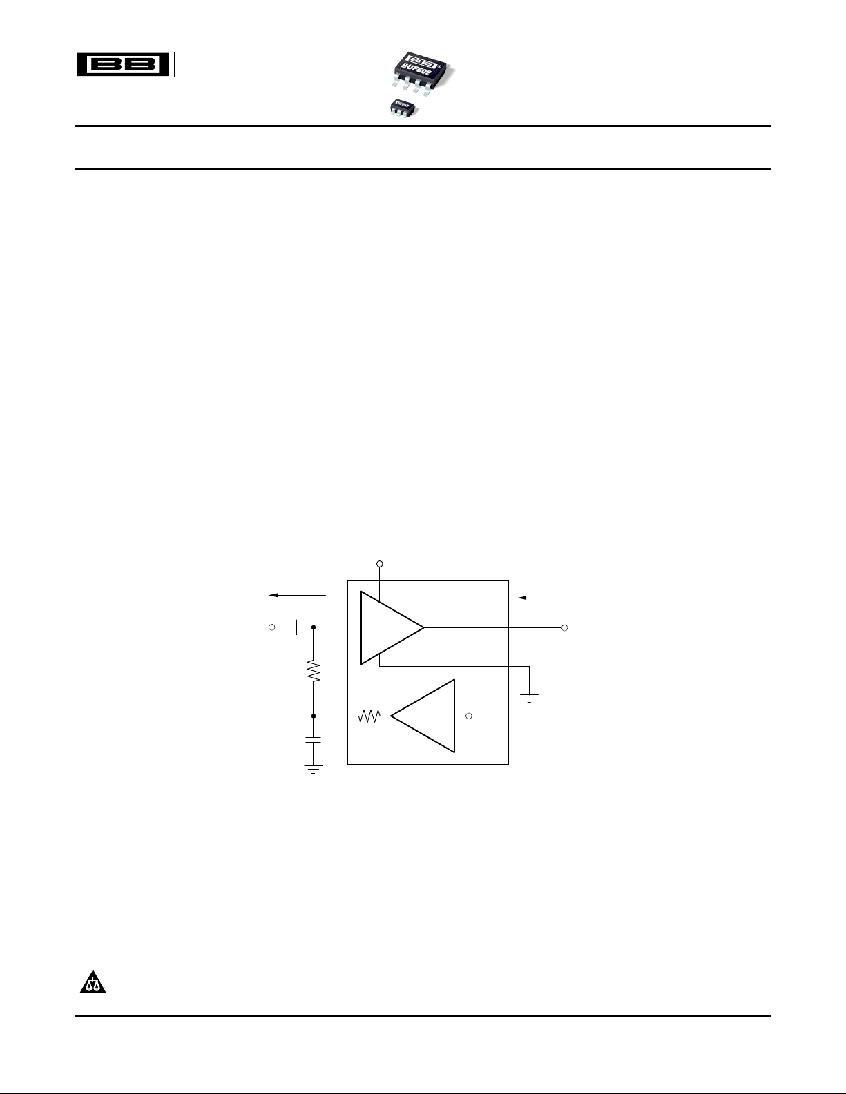
Self-Referenced, AC-Coupled, Single-Supply Buffer
x1
+V
CC
x1
2k
Ω
V
OUT
V
IN
≈2kΩ
Input Z
ZO< 2Ωto 20MHz
VCC/2
1µF
200
Ω
High-Speed, Closed-Loop Buffer
FEATURES DESCRIPTION
• Wide Bandwidth: 1000MHz
• High Slew Rate: 8000V/ µ s
• Flexible Supply Range:
± 1.4V to ± 6.3V Dual Supplies
+2.8V to +12.6V Single Supply
• Output Current: 60mA (continuous)
• Peak Output Current: 350mA
• Low Quiescent Current: 5.8mA
• Standard Buffer Pinout
• Optional Mid-Supply Reference Buffer
APPLICATIONS
• Low Impedance Reference Buffers
• Clock Distribution Circuits
• Video/Broadcast Equipment
• Communications Equipment
• High-Speed Data Acquisition
• Test Equipment and Instrumentation
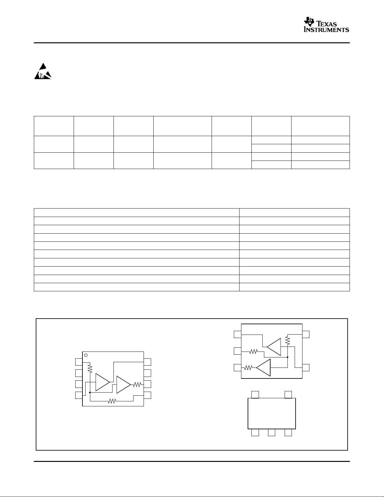
BUF602
SBOS339 – OCTOBER 2005
The BUF602 is a closed-loop buffer recommended for
a wide range of applications. Its wide bandwidth
(1000MHz) and high slew rate (8000V/ µ s) make it
ideal for buffering very high-frequency signals. For
AC-coupled applications, an optional mid-point
reference (V
external components required and the necessary
supply current to provide that reference.
The BUF602 is available in a standard SO-8
surface-mount package and in an SOT23-5 where a
smaller footprint is needed.
) is provided, reducing the number of
REF
All trademarks are the property of their respective owners.
PRODUCTION DATA information is current as of publication date.
Products conform to specifications per the terms of the Texas
Instruments standard warranty. Production processing does not
necessarily include testing of all parameters.
Please be aware that an important notice concerning availability, standard warranty, and use in critical applications of Texas
Instruments semiconductor products and disclaimers thereto appears at the end of this data sheet.
Copyright © 2005, Texas Instruments Incorporated
Page 2
www.ti.com
Top View
1
2
3
5
4
Out
−V
CC
V
REF
+V
CC
In
AWO
1
2
3
5
4
PinOrientation/Package Marking
SOT23−5
x1
x1
200Ω
50kΩ
50kΩ
1
2
3
4
8
7
6
5
+V
CC
NC
NC
In
Out
NC
V
REF
−V
CC
SO−8
NC= NoConnection
x1
x1
200Ω
50kΩ
50kΩ
BUF602
SBOS339 – OCTOBER 2005
This integrated circuit can be damaged by ESD. Texas Instruments recommends that all integrated
circuits be handled with appropriate precautions. Failure to observe proper handling and installation
procedures can cause damage.
ESD damage can range from subtle performance degradation to complete device failure. Precision
integrated circuits may be more susceptible to damage because very small parametric changes could
cause the device not to meet its published specifications.
ORDERING INFORMATION
(1)
SPECIFIED
PACKAGE TEMPERATURE PACKAGE ORDERING TRANSPORT MEDIA,
PRODUCT PACKAGE DESIGNATOR RANGE MARKING NUMBER QUANTITY
BUF602 SO-8 D –45 ° C to +85 ° C BUF602
BUF602 SOT23-5 DBV –45 ° C to +85 ° C AWO
BUF602ID Rails, 75
BUF602IDR Tape and Reel, 2500
BUF602IDBVT Tape and Reel, 250
BUF602IDBVR Tape and Reel, 3000
(1) For the most current package and ordering information, see the Package Option Addendum at the end of this document or see the TI
web site at www.ti.com .
ABSOLUTE MAXIMUM RATINGS
(1)
Power Supply ± 6.5V
Internal Power Dissipation See Thermal Information
Input Common-Mode Voltage Range ± V
Storage Temperature Range: D, DBV –40 ° C to +125 ° C
Lead Temperature (soldering, 10s) +300 ° C
Junction Temperature (TJ) +150 ° C
ESD Rating:
Human Body Model (HBM) 2000V
Charge Device Model (CDM) 1000V
Machine Model (MM) 200V
(1) Stresses above these ratings may cause permanent damage. Exposure to absolute maximum conditions for extended periods may
degrade device reliability. These are stress ratings only, and functional operation of the device at these or any other conditions beyond
those specified is not supported.
DC
S
2
Page 3

www.ti.com
SBOS339 – OCTOBER 2005
BUF602
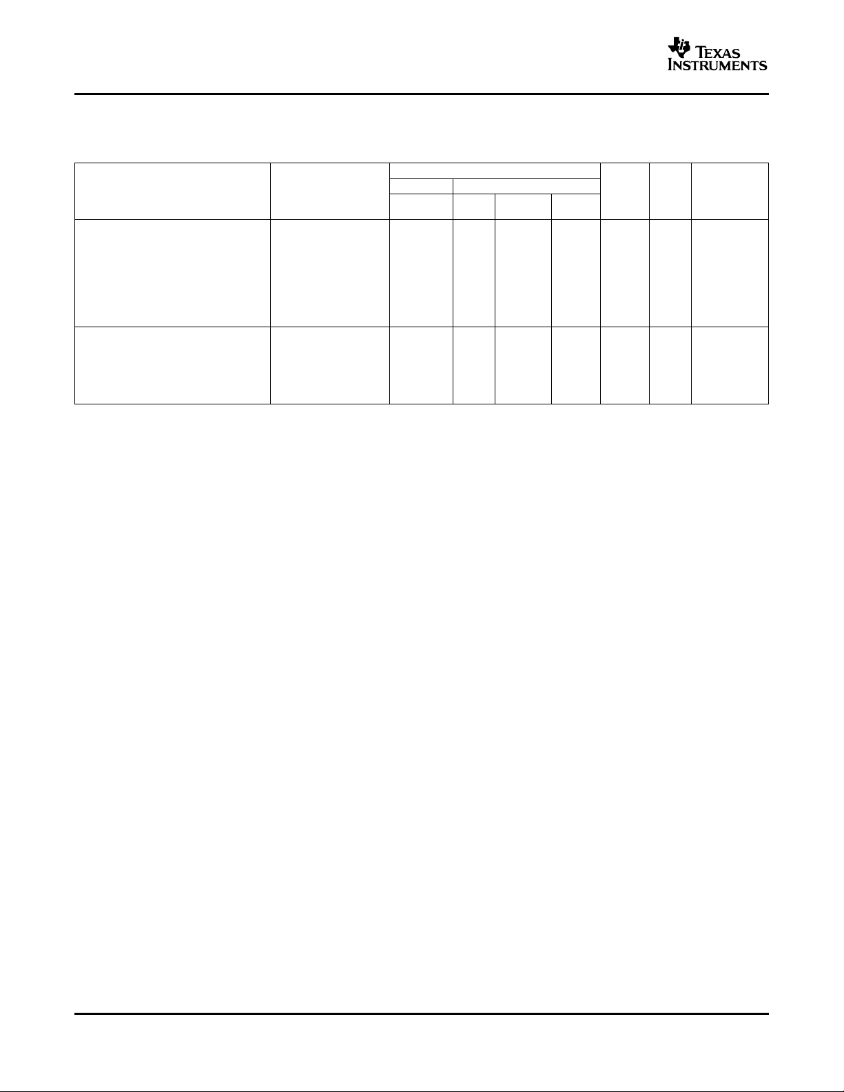
ELECTRICAL CHARACTERISTICS: V
= ± 5V
S
Boldface limits are tested at +25 ° C.
At RL= 100 Ω , unless otherwise noted.
BUF602ID, IDBV
TYP MIN/MAX OVER TEMPERATURE
0 ° C to –40 ° C to MIN/
PARAMETER CONDITIONS +25 ° C +25 ° C
AC PERFORMANCE (See figure 30)
Bandwidth VO= 500mV
Full Power Bandwidth VO= 5V
Bandwidth for 0.1dB Flatness VO= 500mV
Slew Rate VO= 5V Step 8000 7000 6000 5000 V/ µ s min B
Rise Time and Fall Time VO= 0.2V Step 350 625 640 650 ps max B
Settling Time to 0.05% VO= 1V Step 6 ns typ C
Harmonic Distortion VO= 2V
2nd-Harmonic RL= 100 Ω –57 –44 –44 –42 dBc max B
3rd-Harmonic RL= 100 Ω –68 –63 –63 –63 dBc max B
Input Voltage Noise f > 100kHz 4.8 5.1 5.6 6.0 nV/ √ Hz max B
Input Current Noise f > 100kHz 2.1 2.6 2.7 2.8 pA/ √ Hz max B
Differential Gain NTSC, RL= 150 Ω to 0V 0.15 % typ C
Differential Phase NTSC, RL= 150 Ω to 0V 0.04 ° typ C
BUFFER DC PERFORMANCE
Maximum Gain RL= 500 Ω 0.99 1 1 1 V/V max A
Minimum Gain RL= 500 Ω 0.99 0.98 0.98 0.98 V/V min A
Input Offset Voltage ± 16 ± 30 ± 36 ± 38 mV max A
Average Input Offset Voltage Drift ± 125 ± 125 µ V/ ° C max B
Input Bias Current ± 3 ± 7 ± 8 ± 8.5 µ A max A
Average Input Bias Current Drift ± 20 ± 20 nA/ ° C max B
BUFFER INPUT
Input Impedance 1.0 || 2.1 M Ω || pF typ C
BUFFER OUTPUT
Output Voltage Swing RL= 100 Ω ± 3.8 ± 3.7 ± 3.7 ± 3.7 V min B
Output Current (Continuous) VO= 0V ± 60 ± 50 ± 49 ± 48 mA min A
Peak Output Current VO= 0V ± 350 mA typ C
Closed-Loop Output Impedance f ≤ 10MHz 1.4 Ω typ C
POWER SUPPLY
Specified Operating Voltage ± 5 V typ C
Maximum Operating Voltage ± 6.3 ± 6.3 ± 6.3 V max A
Minimum Operating Voltage ± 1.4 ± 1.4 ± 1.4 V min B
Maximum Quiescent Current VS= ± 5V 5.8 6.3 6.9 7.2 mA max A
Minimum Quiescent Current VS= ± 5V 5.8 5.3 4.9 4.3 mA min A
Power-Supply Rejection Ratio (+PSRR) 54 48 46 45 dB min A
(4)
PP
VO= 1V
PP
PP
PP
, 5MHz
PP
RL= 500 Ω –76 –63 –62 –60 dBc max B
RL= 500 Ω –98 –85 –84 –82 dBc max B
RL= 500 Ω ± 4.0 ± 3.8 ± 3.8 ± 3.8 V min A
1000 560 550 540 MHz min B
920 MHz typ C
880 MHz typ C
240 MHz typ C
(2)
(1) Test levels: (A) 100% tested at 25 ° C. Over temperature limits set by characterization and simulation. (B) Limits set by characterization
and simulation. ©) Typical value only for information.
(2) Junction temperature = ambient for 25 ° C specifications.
(3) Junction temperature = ambient at low temperature limit; junction temperature = ambient + 8 ° C at high temperature limit for over
temperature specifications.
(4) Current is considered positive out of node.
(3)
70 ° C
+85 ° C
(3)
UNITS MAX TEST LEVEL
(1)
3
Page 4
www.ti.com
BUF602
SBOS339 – OCTOBER 2005
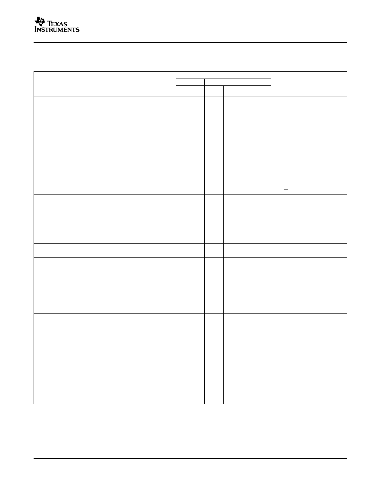
ELECTRICAL CHARACTERISTICS: V
= ± 5V (continued)
S
Boldface limits are tested at +25 ° C.
At RL= 100 Ω , unless otherwise noted.
BUF602ID, IDBV
TYP MIN/MAX OVER TEMPERATURE
0 ° C to –40 ° C to MIN/
PARAMETER CONDITIONS +25 ° C +25 ° C
THERMAL CHARACTERISTICS
Specification: ID –40 to +85 ° C typ C
Thermal Resistance θ
D SO-8 Junction-to-Ambient 125 ° C/W typ C
DBV SOT23-5 Junction-to-Ambient 150 ° C/W typ C
JA
(2)
(3)
70 ° C
+85 ° C
(3)
UNITS MAX TEST LEVEL
(1)
4
Page 5
www.ti.com
SBOS339 – OCTOBER 2005
BUF602
ELECTRICAL CHARACTERISTICS: V
= +5V
S
Boldface limits are tested at +25 ° C.
At RL= 100 Ω to VS/2, unless otherwise noted.
BUF602ID, IDBV
TYP MIN/MAX OVER TEMPERATURE
0 ° C to –40 ° C to MIN/
PARAMETER CONDITIONS +25 ° C +25 ° C
AC PERFORMANCE (See figure 31)
Bandwidth VO= 500mV
Full-Power Bandwidth VO= 3V
Bandwidth for 0.1dB Flatness VO= 500mV
Slew Rate VO= 3V Step 2500 1800 1600 1400 V/ µ s min B
Rise Time and Fall Time VO= 0.2V Step 450 875 875 900 ps max B
Settling Time to 0.05% VO= 1V Step 6 ns typ C
Harmonic Distortion VO= 2V
2nd-Harmonic RL= 100 Ω –50 –45 –44 –43 dBc max B
3rd-Harmonic RL= 100 Ω –70 –64 –64 –63 dBc max B
Input Voltage Noise f > 100kHz 4.9 5.2 5.7 6.1 nV/ √ Hz max B
Input Current Noise f > 100kHz 2.2 2.7 2.8 2.9 pA/ √ Hz max B
Differential Gain NTSC, RL= 100 Ω to VS/2 0.16 % typ C
Differential Phase NTSC, RL= 100 Ω to VS/2 0.05 ° typ C
BUFFER DC PERFORMANCE
Maximum Gain RL= 500 Ω 0.99 1 1 1 V/V max A
Minimum Gain RL= 500 Ω 0.99 0.98 0.98 0.98 V/V min A
Input Offset Voltage ± 16 ± 30 ± 36 ± 38 mV max A
Average Input Offset Voltage Drift ± 125 ± 125 µ V/ ° C max B
Input Bias Current ± 3 ± 7 ± 8 ± 8.5 µ A max A
Average Input Bias Current Drift ± 20 ± 20 nA/ ° C max B
BUFFER INPUT
Input Impedance 1.0 || 2.1 M Ω || pF typ C
BUFFER OUTPUT
Most Positive Output Voltage RL= 100 Ω +3.9 +3.7 +3.7 +3.7 V min B
Least Positive Output Voltage RL= 100 Ω +1.1 +1.3 +1.3 +1.3 V max B
Output Current (Continuous) VO= 0V ± 60 ± 50 ± 49 ± 48 mA min A
Peak Output Current VO= 0V ± 160 mA typ C
Closed-Loop Output Impedance f ≤ 10MHz 1.4 Ω typ C
MID-POINT REFERENCE OUTPUT
Maximum Mid Supply Reference Voltage 2.5 2.6 2.6 2.6 V max A
Minimum Mid Supply Reference Voltage 2.5 2.4 2.4 2.4 V min A
Mid-Supply Output Current, Sourcing 800 µ A typ C
Mid-Supply Output Current, Sinking 70 µ A typ C
Mid-Supply Output Impedance 200 Ω typ C
(4)
PP
VO= 1V
PP
PP
PP
, 5MHz
PP
RL= 500 Ω –73 –62 –61 –60 dBc max B
RL= 500 Ω –73 –72 –72 –71 dBc max B
RL= 500 Ω +4.1 +3.8 +3.8 +3.8 V min A
RL= 500 Ω +0.9 +1.2 +1.2 +1.2 V max A
780 400 400 390 MHz min B
700 MHz typ C
420 MHz typ C
130 MHz typ C
(2)
(1) Test levels: (A) 100% tested at 25 ° C. Over temperature limits set by characterization and simulation. (B) Limits set by characterization
and simulation. ©) Typical value only for information.
(2) Junction temperature = ambient for 25 ° C specifications.
(3) Junction temperature = ambient at low temperature limit; junction temperature = ambient + 4 ° C at high temperature limit for over
temperature specifications.
(4) Current is considered positive out of node.
(3)
70 ° C
+85 ° C
(3)
UNITS MAX TEST LEVEL
(1)
5
Page 6
www.ti.com
BUF602
SBOS339 – OCTOBER 2005
ELECTRICAL CHARACTERISTICS: V
= +5V (continued)
S
Boldface limits are tested at +25 ° C.
At RL= 100 Ω to VS/2, unless otherwise noted.
BUF602ID, IDBV
TYP MIN/MAX OVER TEMPERATURE
0 ° C to –40 ° C to MIN/
PARAMETER CONDITIONS +25 ° C +25 ° C
POWER SUPPLY
Specified Operating Voltage +5 V typ C
Maximum Operating Voltage +12.6 +12.6 +12.6 V max A
Minimum Operating Voltage +2.8 +2.8 +2.8 V min B
Maximum Quiescent Current VS= +5V 5.3 5.8 6.3 6.5 mA max A
Minimum Quiescent Current VS= +5V 5.3 4.8 4.5 3.9 mA min A
Power-Supply Rejection Ratio (+PSRR) 52 46 44 43 dB min A
THERMAL CHARACTERISTICS
Specification: ID –40 to +85 ° C typ C
Thermal Resistance θ
D SO-8 Junction-to-Ambient 125 ° C/W typ C
DBV SOT23-5 Junction-to-Ambient 150 ° C/W typ C
JA
(2)
(3)
70 ° C
+85 ° C
(3)
UNITS MAX TEST LEVEL
(1)
6
Page 7
www.ti.com
SBOS339 – OCTOBER 2005
BUF602
ELECTRICAL CHARACTERISTICS: V
= +3.3V
S
Boldface limits are tested at +25 ° C.
At RL= 100 Ω , unless otherwise noted.
BUF602ID, IDBV
TYP MIN/MAX OVER TEMPERATURE
0 ° C to –40 ° C to MIN/
PARAMETER CONDITIONS +25 ° C +25 ° C
AC PERFORMANCE
Bandwidth VO= 500mV
Full Power Bandwidth VO= 1V
Bandwidth for 0.1dB Flatness VO= 500mV
Slew Rate VO= 1.4V Step 800 650 600 600 V/ µ s min B
Rise Time and Fall Time VO= 0.2V Step 580 1100 1100 1150 ps max B
Settling Time to 0.05% VO= 1V Step 6.5 ns typ C
Harmonic Distortion VO= 1V
2nd-Harmonic RL= 100 Ω –59 –49 –49 –48 dBc max B
3rd-Harmonic RL= 100 Ω –70 –51 –48 –44 dBc max B
Input Voltage Noise f > 100kHz 4.9 5.2 5.7 6.1 nV/ √ Hz max B
Input Current Noise f > 100kHz 2.2 2.7 2.8 2.9 pA/ √ Hz max B
BUFFER DC PERFORMANCE
Maximum Gain RL= 500 Ω 0.99 1 1 1 V/V max A
Minimum Gain RL= 500 Ω 0.99 0.98 0.98 0.98 V/V min A
Input Offset Voltage ± 16 ± 30 ± 36 ± 38 mV max A
Average Input Offset Voltage Drift ± 125 ± 125 µ V/ ° C max B
Input Bias Current ± 3 ± 7 ± 8 ± 8.5 µ A max A
Average Input Bias Current Drift ± 20 ± 20 nA/ ° C max B
BUFFER INPUT
Input Impedance 1.0 || 2.1 M Ω || pF typ C
BUFFER OUTPUT
Most Positive Output Voltage RL= 100 Ω +2.1 +2.0 +2.0 +2.0 V min B
Least Positive Output Voltage RL= 100 Ω +1.2 +1.3 +1.3 +1.3 V max B
Output Current (Continuous) VO= 0 ± 60 ± 50 ± 49 ± 48 mA min A
Peak Output Current ± 100 mA typ C
Closed-Loop Output Impedance f ≤ 10MHz 1.4 Ω typ C
MID-POINT REFERENCE OUTPUT
Maximum Mid Supply Reference Voltage 1.65 1.72 1.72 1.72 V max A
Minimum Mid Supply Reference Voltage 1.65 1.58 1.58 1.58 V min A
Mid Supply Output Current, Sourcing 500 µ A typ C
Mid Supply Output Current, Sinking 60 µ A typ C
Mid Supply Output Impedance 200 Ω typ C
POWER SUPPLY
Specified Operating Voltage +3.3 V typ C
Maximum Operating Voltage +12.6 +12.6 +12.6 V max A
Minimum Operating Voltage +2.8 +2.8 +2.8 V min B
Maximum Quiescent Current VS= +3.3V 5.0 5.5 6.0 6.3 mA max A
Minimum Quiescent Current VS= +3.3V 5.0 4.5 4.2 3.8 mA min A
Power-Supply Rejection Ratio (+PSRR) 50 44 42 41 dB min A
(4)
PP
PP
PP
, 5MHz
PP
RL= 500 Ω –76 –61 –57 –53 dBc max B
RL= 500 Ω –63 –51 –48 –44 dBc max B
RL= 500 Ω +2.3 +2.2 +2.2 +2.2 V min A
RL= 500 Ω +1.0 +1.1 +1.1 +1.1 V max A
600 320 320 310 MHz min B
520 MHz typ C
110 MHz typ C
(2)
(1) Test levels: (A) 100% tested at 25 ° C. Over temperature limits set by characterization and simulation. (B) Limits set by characterization
and simulation. ©) Typical value only for information.
(2) Junction temperature = ambient for 25 ° C specifications.
(3) Junction temperature = ambient at low temperature limit; junction temperature = ambient + 2 ° C at high temperature limit for over
temperature specifications.
(4) Current is considered positive out of node.
(3)
70 ° C
+85 ° C
(3)
UNITS MAX TEST LEVEL
(1)
7
Page 8

www.ti.com
BUF602
SBOS339 – OCTOBER 2005
ELECTRICAL CHARACTERISTICS: V
= +3.3V (continued)
S
Boldface limits are tested at +25 ° C.
At RL= 100 Ω , unless otherwise noted.
BUF602ID, IDBV
TYP MIN/MAX OVER TEMPERATURE
0 ° C to –40 ° C to MIN/
PARAMETER CONDITIONS +25 ° C +25 ° C
THERMAL CHARACTERISTICS
Specification: ID –40 to +85 ° C typ C
Thermal Resistance θ
D SO-8 Junction-to-Ambient 125 ° C/W typ C
DBV SOT23-5 Junction-to-Ambient 150 ° C/W typ C
JA
(2)
(3)
70 ° C
+85 ° C
(3)
UNITS MAX TEST LEVEL
(1)
8
Page 9

www.ti.com
3
0
−
3
−
6
−
9
−
12
−
15
−
18
Frequency (Hz)
1M 10M 100M 1G 2G
Gain (dB)
VO= 2V
PP
VO= 5V
PP
VO= 0.5V
PP
VO= 4V
PP
VO= 0.2V
PP
VO= 1V
PP
RL= 100
Ω
6
3
0
−
3
−
6
−
9
Frequency (Hz)
1M 10M 100M 1G 2G
Gain (dB)
RL= 1k
Ω
RL= 500
Ω
R
L
= 100
Ω
V
OUT
= 0.5V
PP
0.5
0.4
0.3
0.2
0.1
0
−
0.1
−
0.2
−
0.3
−
0.4
−
0.5
Frequency (Hz)
1M 10M 100M
1G
Gain (dB)
VO= 0.5V
PP
RL= 100
Ω
100
10
1
Frequency (Hz)
100 1k 10k 100k 1M 10M
Input Voltage Noise Density (nV/
√
Hz)
Input Current Noise Density (pA/
√
Hz)
Input Current Noise (2.1pA/√Hz)
Input Voltage Noise (4.8nV/√Hz)
150
100
50
0
−
50
−
100
−
150
Time (2ns/div)
Output Voltage (V)
V
OUT
= 0.2V
PP
RL= 100
Ω
f = 40MHz
4
3
2
1
0
−
1
−
2
−
3
−
4
Time (2ns/div)
Output Voltage (V)
V
OUT
= 5V
PP
RL= 100
Ω
f = 40MHz
SBOS339 – OCTOBER 2005
BUF602
TYPICAL CHARACTERISTICS: V
= ± 5V
S
At TA= +25 ° C and RL= 100 Ω , unless otherwise noted.
BUFFER BANDWIDTH vs OUTPUT VOLTAGE BUFFER BANDWIDTH vs LOAD RESISTANCE
Figure 1. Figure 2.
BUFFER GAIN FLATNESS INPUT VOLTAGE AND CURRENT NOISE DENSITY
BUFFER SMALL-SIGNAL PULSE RESPONSE BUFFER LARGE-SIGNAL PULSE RESPONSE
Figure 3. Figure 4.
Figure 5. Figure 6.
9
Page 10

www.ti.com
−
50
−
55
−
60
−
65
−
70
−
75
−
80
−
85
−
90
−
95
−
100
Frequency (MHz)
1 10
100
Harmonic Distortion (dBc)
RL= 500
Ω
VO= 2V
PP
2nd−Harmonic
3rd−Harmonic
−
50
−
60
−
70
−
80
−
90
−
100
Load Resistance (Ω)
100 1k
Harmonic Distortion (dBc)
f = 5MHz
VO= 2V
PP
3rd−Harmonic
2nd−Harmonic
−
60
−
70
−
80
−
90
−
100
−
110
Output Voltage (V
PP
)
0.5 1.0 5.0
Harmonic Distortion (dBc)
1.5 2.0 2.5 3.0 3.5 4.0 4.5
f = 5MHz
RL= 500
Ω
2nd−Harmonic
3rd−Harmonic
−
40
−
50
−
60
−
70
−
80
−
90
−
100
± Supply Voltage
2.0 2.5 6.0
Harmonic Distortion (dBc)
3.0 3.5 4.0 4.5 5.0 5.5
RL= 500
Ω
VO= 2V
PP
2nd−Harmonic
3rd−Harmonic
700
600
500
400
300
200
100
Frequency (MHz)
Group Delay Time (ps)
0 100 200 300 400 500 600 700 800 900 1000
100
10
1
Frequency (Hz)
1k 10k 100k 1M 10M 100M 1G
Output Impedance (
Ω
)
BUF602
SBOS339 – OCTOBER 2005
TYPICAL CHARACTERISTICS: V
At TA= +25 ° C and RL= 100 Ω , unless otherwise noted.
HARMONIC DISTORTION vs FREQUENCY 5MHz HARMONIC DISTORTION vs LOAD RESISTANCE
Figure 7. Figure 8.
HARMONIC DISTORTION vs OUTPUT VOLTAGE 5MHz HARMONIC DISTORTION vs SUPPLY VOLTAGE
= ± 5V (continued)
S
BUFFER OUTPUT IMPEDANCE BUFFER GROUP DELAY TIME vs FREQUENCY
10
Figure 9. Figure 10.
Figure 11. Figure 12.
Page 11

www.ti.com
4.10
4.05
4.00
3.95
3.90
Ambient Temperature (C)
±
Output Voltage Swing (V)
−40−
20 0 20 40 60 80 100 120
+V
O
−
V
O
50
45
40
35
30
25
20
15
10
5
0
Frequency (Hz)
PSRR (dB)
10k 100k 1M 10M 100M
−
PSRR
+PSRR
30
25
20
15
10
5
0
Ambient Temperature (C)
Input Offset Voltage (mV)
6
5
4
3
2
1
0
Input Bias Current (
µ
A)
−40−
20 0 20 40 60 80 100 120
Buffer Input Offset Voltage (VOS)
Buffer Input Bias Current (IB)
5
4
3
2
1
0
−
1
−
2
−
3
−
4
−
5
Output Current (mA)
Output Voltage (V)
−
300
−
250
−
200
−
150
−
100
−
50
0
50
100
150
200
250
300
1W Internal
Power Limit
1W Internal
Power Limit
25ΩLoad Line
50ΩLoad Line
100
Ω
Load Line
SBOS339 – OCTOBER 2005
BUF602
TYPICAL CHARACTERISTICS: V
At TA= +25 ° C and RL= 100 Ω , unless otherwise noted.
POWER-SUPPLY REJECTION RATIO vs FREQUENCY OUTPUT SWING VOLTAGE vs TEMPERATURE
Figure 13. Figure 14.
DC DRIFT vs TEMPERATURE BUFFER OUTPUT VOLTAGE AND CURRENT LIMITATIONS
= ± 5V (continued)
S
Figure 15. Figure 16.
11
Page 12

www.ti.com
3
0
−
3
−
6
−
9
−
12
−
15
−
18
Frequency (Hz)
1M 10M 100M 1G 2G
Gain (dB)
VO= 0.5V
PP
VO= 2V
PP
VO= 3V
PP
VO= 0.2V
PP
VO= 1V
PP
RL= 100
Ω
−
40
−
45
−
50
−
55
−
60
−
65
−
70
−
75
−
80
−
85
−
90
Frequency (MHz)
1 10
100
Harmonic Distortion (dBc)
RL= 500
Ω
VO= 2V
PP
2nd−Harmonic
3rd−Harmonic
0.5
0.4
0.3
0.2
0.1
0
−
0.1
−
0.2
−
0.3
−
0.4
−
0.5
Frequency (MHz)
1 10 100
500
Gain (dB)
V
OUT
= 0.5V
PP
RL= 100
Ω
−
60
−
65
−
70
−
75
−
80
−
85
−
90
Load Resistance (Ω)
100 1k
Harmonic Distortion (dBc)
f = 5MHz
VO= 2V
PP
2nd−Harmonic
3rd−Harmonic
2.8
2.7
2.6
2.5
2.4
2.3
2.2
Time (2ns/div)
Output Voltage (mV)
4.3
3.7
3.1
2.5
1.9
1.3
0.7
Output Voltage (V)
Small−Signal
2.55V
DC
±
0.1V
Left Scale
Large−Signal
2.5V
DC
±
1.5V
Right Scale
RL= 100
Ω
f = 40MHz
−
40
−
50
−
60
−
70
−
80
−
90
−
100
Output Voltage (V
PP
)
0.5 1.0
3.5
Harmonic Distortion (dBc)
1.5 2.0 2.5 3.0
f = 5MHz
RL= 500
Ω
2nd−Harmonic
3rd−Harmonic
BUF602
SBOS339 – OCTOBER 2005
TYPICAL CHARACTERISTICS: V
= +5V
S
At TA= +25 ° C and RL= 100 Ω to VS/2, unless otherwise noted.
BUFFER BANDWIDTH vs OUTPUT VOLTAGE HARMONIC DISTORTION vs FREQUENCY
Figure 17. Figure 18.
BUFFER GAIN FLATNESS 5MHz HARMONIC DISTORTION vs LOAD RESISTANCE
Figure 19. Figure 20.
BUFFER PULSE RESPONSE HARMONIC DISTORTION vs OUTPUT VOLTAGE
12
Figure 21. Figure 22.
Page 13

www.ti.com
3
0
−
3
−
6
−
9
−
12
−
15
−
18
Frequency (Hz)
1M 10M 100M 2G1G
Gain (dB)
VO= 0.5V
PP
VO= 0.2V
PP
VO= 1V
PP
RL= 100
Ω
−
40
−
45
−
50
−
55
−
60
−
65
−
70
−
75
−
80
Frequency (MHz)
1 10
100
Harmonic Distortion (dBc)
RL= 500
Ω
VO= 1V
PP
3rd−Harmonic
2nd−Harmonic
0.5
0.4
0.3
0.2
0.1
0.0
−
0.1
−
0.2
−
0.3
−
0.4
−
0.5
Frequency (MHz)
1 10 100 300
Gain (dB)
VO= 0.5V
PP
RL= 100
Ω
−
50
−
55
−
60
−
65
−
70
−
75
−
80
Load Resistance (Ω)
100 1k
Harmonic Distortion (dBc)
f = 5MHz
VO= 1V
PP
3rd−Harmonic
2nd−Harmonic
2.0
1.9
1.8
1.7
1.6
1.5
1.4
1.3
Time (2ns/div)
Output Voltage (mV)
2.7
2.4
2.1
1.8
1.5
1.2
0.9
0.6
Output Voltage (V)
Small−Signal
1.65V
DC
±
0.1V
Left Scale
Large−Signal
1.65V
DC
±
0.7V
Right Scale
RL= 100
Ω
f = 40MHz
−
30
−
40
−
50
−
60
−
70
−
80
−
90
Output Voltage (V
PP
)
0.50 1.50
Harmonic Distortion (dBc)
0.75 1.00 1.25
f = 5MHz
R
L
= 500
Ω
2nd−Harmonic
3rd−Harmonic
SBOS339 – OCTOBER 2005
BUF602
TYPICAL CHARACTERISTICS: V
= +3.3V
S
At TA= +25 ° C and RL= 100 Ω to VS/2, unless otherwise noted.
BUFFER BANDWIDTH vs OUTPUT VOLTAGE HARMONIC DISTORTION vs FREQUENCY
Figure 23. Figure 24.
BUFFER GAIN FLATNESS 5MHz HARMONIC DISTORTION vs LOAD RESISTANCE
Figure 25. Figure 26.
BUFFER PULSE RESPONSE HARMONIC DISTORTION vs OUTPUT VOLTAGE
Figure 27. Figure 28.
13
Page 14

www.ti.com
V
CC
To VCC/2
BUF602
2k
Ω
50
Ω
0.1µF
50ΩLoad
V
OUT
VCC/2
0.1µF
200
Ω
50
Ω
+
50
Ω
BUF602
50
Ω
V
IN
50ΩSource
V
OUT
50ΩLoad
0.1µF 4.7µF
−
5V
+
0.1µF 4.7µF
+5V
Z
0
L
T
C
T
BUF602
SBOS339 – OCTOBER 2005
APPLICATION INFORMATION
WIDEBAND BUFFER OPERATION
The BUF602 gives the exceptional AC performance
of a wideband buffer. Requiring only 5.8mA quiescent
current, the BUF602 will swing to within 1V of either
supply rail and deliver in excess of 60mA at room
temperature. This low output headroom requirement,
along with supply voltage independent biasing, gives
remarkable single (+5V) supply operation. The
BUF602 will deliver greater than 500MHz bandwidth
driving a 2V
supply.
Figure 29 shows the DC-coupled, dual power-supply
circuit configuration used as the basis of the ± 5V
Electrical and Typical Characteristics. For test
purposes, the input impedance is set to 50 Ω with a
resistor to ground and the output impedance is set to
50 Ω with a series output resistor. Voltage swings
reported in the specifications are taken directly at the
input and output pins while load powers (dBm) are
defined at a matched 50 Ω load. In addition to the
usual power-supply decoupling capacitors to ground,
a 0.01 µ F capacitor can be included between the two
power-supply pins. This optional added capacitor will
typically improve the 2nd-harmonic distortion
performance by 3dB to 6dB.
output into 100 Ω on a single +5V
PP
bandwidth. The key requirement of broadband
single-supply operation of the BUF602 is to maintain
output signal swings within the usable voltage ranges.
The circuit of Figure 30 establishes an input midpoint
bias using the internal mid-point reference. The input
signal is then AC-coupled into this mid-point voltage
bias. Again, on a single +5V supply, the output
voltage can swing to within 1V of either supply pin
while delivering more than 60mA output current. A
demanding 100 Ω load to a mid-point bias is used in
this characterization circuit.
Figure 30. AC-Coupled, Single-Supply,
Specification and Test Circuit
Figure 29. DC-Coupled, Bipolar Supply,
Specification and Test Circuit
Figure 30 shows the AC-coupled, single-supply circuit
configuration used as the basis of the +5V Electrical
and Typical Characteristics. Though not a rail-to-rail
design, the BUF602 requires minimal input and
output voltage headroom compared to other very
wideband buffers. It will deliver a 3V
on a single +5V supply with greater than 400MHz
14
LOW-IMPEDANCE TRANSMISSION LINES
The most important equations and technical basics of
transmission lines support the results found for the
various drive circuits presented here. An ideal
transmission medium with zero ohmic impedance
would have inductance and capacitance distributed
over the transmission cable. Both inductance and
capacitance detract from the transmission quality of a
line. Each input is connected with high impedance to
the line as in a daisy chain or loop-through
configuration, and each adds capacitance of at least
a few picofarad. The typical transmission line
impedance (Z
the impedance is calculated by the square root of line
inductance (L
output swing
PP
) defines the line type. In Equation 1 ,
O
) divided by line capacitance ©T):
T
(1)
Page 15

www.ti.com
LT C
T
R
LOAD
R
OUT
Z
O
V
IN
V
OUT
BUF602
VT V
OUT
V
REFL
V
REFL
V
OUT
50k
Ω
50k
Ω
V
S
VS/2
BUF602
200
Ω
0.1µF
20
Ω
x1
x1
Z1 Z
0
Z1 Z
0
In the same manner, line inductance and capacitance
determine the delay time of a transmission line as
shown in Equation 2 :
Typical values for Z
and 75 Ω or 50 Ω for coax cables. Z
are 240 Ω for symmetrical traces
O
sometimes
O
decreases to 30 Ω to 40 Ω in high data rate bus
systems for bus lines on printed circuit boards
(PCBs). In general, the more complex a bus system
is, the lower Z
will be. Because it increases the
O
capacitance of the transmission medium, a complex
system lowers the typical line impedance, resulting in
higher drive requirements for the line drivers used
here.
Transmission lines are almost always terminated on
the transmitter line and always terminated on the
receiver side. Unterminated lines generate signal
reflections that degrade the pulse fidelity. The driver
circuit transmits the output voltage (V
) over the
OUT
line. The signal appears at the end of the line and will
be reflected when not properly terminated. The
reflected portion of V
OUT
, called V
REFL
, returns to the
driver. The transmitted signal is the sum of the
original signal V
and the reflected V
OUT
.
REFL
The magnitude of the reflected signal depends upon
the typical line impedance (Z
) and the value of the
0
termination resistor Z1.
Γ denotes the reflection factor and is described by
Equation 5 .
BUF602
SBOS339 – OCTOBER 2005
(2)
Figure 31. Typical Line Driver Circuit
SELF-BIASED, LOW-IMPEDANCE MID SUPPLY VOLTAGE REFERENCE
Using the mid-point reference in conjunction with the
BUF602 allows the creation of a low-impedance
reference from DC to 250MHz.
The 0.1 µ F external capacitor is used in Figure 32 to
filter the noise.
(3)
(4)
Γ can vary from –1 to +1.
The conditions at the corner points of Equation 5 are
as follows:
Z0= Z
1
Z0= ∞ → Γ = –1 V
Z0= 0 → Γ = +1 V
→ Γ = 0 V
= 0
REFL
= –V
REFL
REFL
OUT
= +V
OUT
An unterminated driver circuit complicates the
situation even more. V
is reflected a second time
REFL
on the driver side and wanders like a ping-pong ball
back and forth over the line. When this happens, it is
usually impossible to recover the output signal V
on the receiver side.
The figure shown in Figure 31 makes use of the
BUF602 as a line driver. The BUF602 exhibits high
input impedance and low output impedance, making it
ideal whenever a buffer is required.
(5)
Figure 32. Self-Biased, Low Impedance Mid
Supply Voltage Reference
SELF-REFERENCED, AC-COUPLED WIDEBAND BUFFER
Whenever a high-speed AC-coupled buffer is
required, you should consider the BUF602. One
feature of the BUF602 is the mid-supply reference
voltage, saving external components and power
dissipation. A capacitor on the output of the
mid-supply reference is recommended to bandlimit
the noise contribution of the mid-supply reference
voltage generated by the two 50k Ω internal resistors.
OUT
This circuit is shown on the front page of the
datasheet.
15
Page 16

www.ti.com
e
n
i
n
R
S
√
4kTR
S
e
O
eO e
2
n
inR
S
2
4kTR
S
nV
Hz
BUF602
SBOS339 – OCTOBER 2005
DESIGN-IN TOOLS
DEMONSTRATION BOARDS
Two PC boards are available to assist in the initial
evaluation of circuit performance using the BUF602 in
its two package styles. Both are available free, as
unpopulated PC boards delivered with descriptive
documentation. The summary information for these
boards is shown in Table 1 .
Table 1. Demo Board Listing
PRODUCT GE NUMBER NUMBER
PACKA BOARD PART REQUEST
BUF602ID SO-8 DEM-BUF-SO-1A SBAU118
BUF602IDBV SOT23-5 DEM-BUF-SOT-1A SBAU117
LITERATURE
To request either of these boards, use the Texas
Instruments web site (www.ti.com ).
MACROMODELS AND APPLICATIONS SUPPORT
Computer simulation of circuit performance using
SPICE is often useful when analyzing the
performance of analog circuits and systems. This is
particularly true for video and RF amplifier circuits
where parasitic capacitance and inductance can have
a major effect on circuit performance. A SPICE model
for the BUF602 is available through the TI web site
(www.ti.com ). These models do a good job of
predicting small-signal AC and transient performance
under a wide variety of operating conditions. They do
not do as well in predicting the harmonic distortion or
dG/dP characteristics. These models do not attempt
to distinguish between package types in their
small-signal AC performance.
OUTPUT CURRENT AND VOLTAGE
The BUF602 provides output voltage and current
capabilities that are not usually found in wideband
buffers. Under no-load conditions at 25 ° C, the output
voltage typically swings closer than 1.2V to either
supply rail; the +25 ° C swing limit is within 1.2V of
either rail. Into a 15 Ω load (the minimum tested load),
it is tested to deliver more than ± 60mA.
The specifications described above, though familiar in
the industry, consider voltage and current limits
separately. In many applications, it is the voltage ×
current, or V-I product, which is more relevant to
circuit operation. Refer to the Buffer Output Voltage
and Current Limitations plot (Figure 16 ) in the Typical
Characteristics. The X and Y axes of this graph show
the zero-voltage output current limit and the
zero-current output voltage limit, respectively. The
four quadrants give a more detailed view of the
BUF602 output drive capabilities, noting that the
16
graph is bounded by a Safe Operating Area of 1W
maximum internal power dissipation. Superimposing
resistor load lines onto the plot shows that the
BUF602 can drive ± 3V into 25 Ω or ± 3.5V into 50 Ω
without exceeding the output capabilities or the 1W
dissipation limit.
The minimum specified output voltage and current
over-temperature are set by worst-case simulations at
the cold temperature extreme. Only at cold startup
will the output current and voltage decrease to the
numbers shown in the Electrical Characteristic tables.
As the output transistors deliver power, the junction
temperatures will increase, decreasing both V
(increasing the available output voltage swing) and
increasing the current gains (increasing the available
output current). In steady-state operation, the
available output voltage and current will always be
greater than that shown in the over-temperature
specifications, since the output stage junction
temperatures will be higher than the minimum
specified operating ambient.
For a buffer, the noise model is shown in Figure 33 .
Equation 6 shows the general form for the output
noise voltage using the terms shown in Figure 33 .
Figure 33. Buffer Noise Analysis Model
THERMAL ANALYSIS
Due to the high output power capability of the
BUF602, heatsinking or forced airflow may be
required under extreme operating conditions.
Maximum desired junction temperature will set the
maximum allowed internal power dissipation as
described below. In no case should the maximum
junction temperature be allowed to exceed 150 ° C.
Operating junction temperature (T
P
× θJA. The total internal power dissipation (P
D
the sum of quiescent power (P
power dissipated in the output stage (P
load power. Quiescent power is simply the specified
no-load supply current times the total supply voltage
across the part. P
will depend on the required
DL
) is given by T
J
) and additional
DQ
) to deliver
DL
A
) is
D
BE
(6)
+
Page 17

www.ti.com
BUF602
SBOS339 – OCTOBER 2005
output signal and load but would, for a grounded and ground traces to minimize inductance between
resistive load, be at a maximum when the output is the pins and the decoupling capacitors. The
fixed at a voltage equal to ½ of either supply voltage power-supply connections should always be
(for equal bipolar supplies). Under this condition, P
2
= V
/(4 × RL). decoupling capacitor (0.1µF) across the two power
S
DL
Note that it is the power in the output stage and not
into the load that determines internal power
dissipation.
As a worst-case example, compute the maximum T
using a BUF602IDBV in the circuit on the front page
operating at the maximum specified ambient
temperature of +85 ° C and driving a grounded 20 Ω
load.
P
= 10V × 5.8mA + 52/(4 × 20 Ω ) = 370.5mW
D
Maximum TJ= +85 ° C + (0.37W × 150 ° C/W) = 141 ° C.
Although this is still below the specified maximum
junction temperature, system reliability considerations
may require lower tested junction temperatures. The
highest possible internal dissipation will occur if the
load requires current to be forced into the output for
positive output voltages or sourced from the output
for negative output voltages. This puts a high current
through a large internal voltage drop in the output
transistors. The output V-I plot (Figure 16 ) shown in
the Typical Characteristics include a boundary for 1W
maximum internal power dissipation under these
conditions.
BOARD LAYOUT GUIDELINES
Achieving optimum performance with a
high-frequency amplifier like the BUF602 requires
careful attention to board layout parasitics and
external component types. Recommendations that
will optimize performance include:
a) Minimize parasitic capacitance to any AC ground
for all of the signal I/O pins. Parasitic capacitance on
the output pins can cause instability: on the
noninverting input, it can react with the source
impedance to cause unintentional bandlimiting. To
reduce unwanted capacitance, a window around the
signal I/O pins should be opened in all of the ground
and power planes around those pins. Otherwise,
ground and power planes should be unbroken
elsewhere on the board.
b) Minimize the distance (< 0.25") from the
power-supply pins to high-frequency 0.1µF
decoupling capacitors. At the device pins, the ground
and power-plane layout should not be in close
proximity to the signal I/O pins. Avoid narrow power
decoupled with these capacitors. An optional supply
supplies (for bipolar operation) will improve
2nd-harmonic distortion performance. Larger (2.2µF
to 6.8µF) decoupling capacitors, effective at lower
frequency, should also be used on the main supply
pins. These may be placed somewhat farther from
J
the device and may be shared among several
devices in the same area of the PC board.
c) Careful selection and placement of external
components will preserve the high-frequency
performance of the BUF602. Resistors should be a
very low reactance type. Surface-mount resistors
work best and allow a tighter overall layout. Metal film
or carbon composition, axially-leaded resistors can
also provide good high-frequency performance.
Again, keep their leads and PC board traces as short
as possible. Never use wirewound type resistors in a
high-frequency application.
d) Connections to other wideband devices on the
board may be made with short, direct traces or
through onboard transmission lines. For short
connections, consider the trace and the input to the
next device as a lumped capacitive load. Relatively
wide traces (50mils to 100mils) should be used,
preferably with ground and power planes opened up
around them. If a long trace is required, and the 6dB
signal loss intrinsic to a doubly-terminated
transmission line is acceptable, implement a matched
impedance transmission line using microstrip or
stripline techniques (consult an ECL design handbook
for microstrip and stripline layout techniques). A 50 Ω
environment is normally not necessary on board, and
in fact, a higher impedance environment will improve
distortion as shown in the distortion versus load plots.
e) Socketing a high-speed part like the BUF602 is
not recommended. The additional lead length and
pin-to-pin capacitance introduced by the socket can
create an extremely troublesome parasitic network
that makes it almost impossible to achieve a smooth,
stable frequency response. Best results are obtained
by soldering the BUF602 onto the board.
17
Page 18

www.ti.com
External
Pin
+V
CC
−
V
CC
Internal
Circuitry
BUF602
SBOS339 – OCTOBER 2005
INPUT AND ESD PROTECTION
The BUF602 is built using a very high-speed
complementary bipolar process. The internal junction
breakdown voltages are relatively low for these very
small geometry devices. These breakdowns are
reflected in the Absolute Maximum Ratings table. All
device pins are protected with internal ESD protection
diodes to the power supplies as shown in Figure 34 .
Figure 34. Internal ESD Protection
These diodes provide moderate protection to input
overdrive voltages above the supplies as well. The
protection diodes can typically support 30mA
continuous current. Where higher currents are
possible (for example, in systems with ± 15V supply
parts driving into the BUF602), current-limiting series
resistors should be added into the two inputs. Keep
these resistor values as low as possible since high
values degrade both noise performance and
frequency response.
18
Page 19

PACKAGE OPTION ADDENDUM
www.ti.com
7-Nov-2005
PACKAGING INFORMATION
Orderable Device Status
(1)
Package
Type
Package
Drawing
Pins Package
Qty
Eco Plan
BUF602ID ACTIVE SOIC D 8 75 TBD Call TI Call TI
BUF602IDBVR ACTIVE SOT-23 DBV 5 3000 TBD Call TI Call TI
BUF602IDBVT ACTIVE SOT-23 DBV 5 250 TBD Call TI Call TI
BUF602IDR ACTIVE SOIC D 8 2500 TBD Call TI Call TI
(1)
The marketing status values are defined as follows:
ACTIVE: Product device recommended for new designs.
LIFEBUY: TI has announced that the device will be discontinued, and a lifetime-buy period is in effect.
NRND: Not recommended for new designs. Device is in production to support existing customers, but TI does not recommend using this part in
a new design.
PREVIEW: Device has been announced but is not in production. Samples may or may not be available.
OBSOLETE: TI has discontinued the production of the device.
(2)
Eco Plan - The planned eco-friendly classification: Pb-Free (RoHS) or Green (RoHS & no Sb/Br) - please check
http://www.ti.com/productcontent for the latest availability information and additional product content details.
TBD: The Pb-Free/Green conversion plan has not been defined.
Pb-Free (RoHS): TI's terms "Lead-Free" or "Pb-Free" mean semiconductor products that are compatible with the current RoHS requirements
for all 6 substances, including the requirement that lead not exceed 0.1% by weight in homogeneous materials. Where designed to be soldered
at high temperatures, TI Pb-Free products are suitable for use in specified lead-free processes.
Green (RoHS & no Sb/Br): TI defines "Green" to mean Pb-Free (RoHS compatible), and free of Bromine (Br) and Antimony (Sb) based flame
retardants (Br or Sb do not exceed 0.1% by weight in homogeneous material)
(2)
Lead/Ball Finish MSL Peak Temp
(3)
(3)
MSL, Peak Temp. -- The Moisture Sensitivity Level rating according to the JEDEC industry standard classifications, and peak solder
temperature.
Important Information and Disclaimer:The information provided on this page represents TI's knowledge and belief as of the date that it is
provided. TI bases its knowledge and belief on information provided by third parties, and makes no representation or warranty as to the
accuracy of such information. Efforts are underway to better integrate information from third parties. TI has taken and continues to take
reasonable steps to provide representative and accurate information but may not have conducted destructive testing or chemical analysis on
incoming materials and chemicals. TI and TI suppliers consider certain information to be proprietary, and thus CAS numbers and other limited
information may not be available for release.
In no event shall TI's liability arising out of such information exceed the total purchase price of the TI part(s) at issue in this document sold by TI
to Customer on an annual basis.
Addendum-Page 1
Page 20

Page 21

Page 22

IMPORTANT NOTICE
Texas Instruments Incorporated and its subsidiaries (TI) reserve the right to make corrections, modifications,
enhancements, improvements, and other changes to its products and services at any time and to discontinue
any product or service without notice. Customers should obtain the latest relevant information before placing
orders and should verify that such information is current and complete. All products are sold subject to TI’s terms
and conditions of sale supplied at the time of order acknowledgment.
TI warrants performance of its hardware products to the specifications applicable at the time of sale in
accordance with TI’s standard warranty. Testing and other quality control techniques are used to the extent TI
deems necessary to support this warranty . Except where mandated by government requirements, testing of all
parameters of each product is not necessarily performed.
TI assumes no liability for applications assistance or customer product design. Customers are responsible for
their products and applications using TI components. To minimize the risks associated with customer products
and applications, customers should provide adequate design and operating safeguards.
TI does not warrant or represent that any license, either express or implied, is granted under any TI patent right,
copyright, mask work right, or other TI intellectual property right relating to any combination, machine, or process
in which TI products or services are used. Information published by TI regarding third-party products or services
does not constitute a license from TI to use such products or services or a warranty or endorsement thereof.
Use of such information may require a license from a third party under the patents or other intellectual property
of the third party, or a license from TI under the patents or other intellectual property of TI.
Reproduction of information in TI data books or data sheets is permissible only if reproduction is without
alteration and is accompanied by all associated warranties, conditions, limitations, and notices. Reproduction
of this information with alteration is an unfair and deceptive business practice. TI is not responsible or liable for
such altered documentation.
Resale of TI products or services with statements different from or beyond the parameters stated by TI for that
product or service voids all express and any implied warranties for the associated TI product or service and
is an unfair and deceptive business practice. TI is not responsible or liable for any such statements.
Following are URLs where you can obtain information on other Texas Instruments products and application
solutions:
Products Applications
Amplifiers amplifier.ti.com Audio www.ti.com/audio
Data Converters dataconverter.ti.com Automotive www.ti.com/automotive
DSP dsp.ti.com Broadband www.ti.com/broadband
Interface interface.ti.com Digital Control www.ti.com/digitalcontrol
Logic logic.ti.com Military www.ti.com/military
Power Mgmt power.ti.com Optical Networking www.ti.com/opticalnetwork
Microcontrollers microcontroller.ti.com Security www.ti.com/security
Telephony www.ti.com/telephony
Video & Imaging www.ti.com/video
Wireless www.ti.com/wireless
Mailing Address: Texas Instruments
Post Office Box 655303 Dallas, Texas 75265
Copyright 2005, Texas Instruments Incorporated
 Loading...