

Page 1
SBOS337A − OCTOBER 2006 − REVISED OCTOBER 2006
Please be aware that an important notice concerning availability, standard warranty, and use in critical applications of Texas Instruments
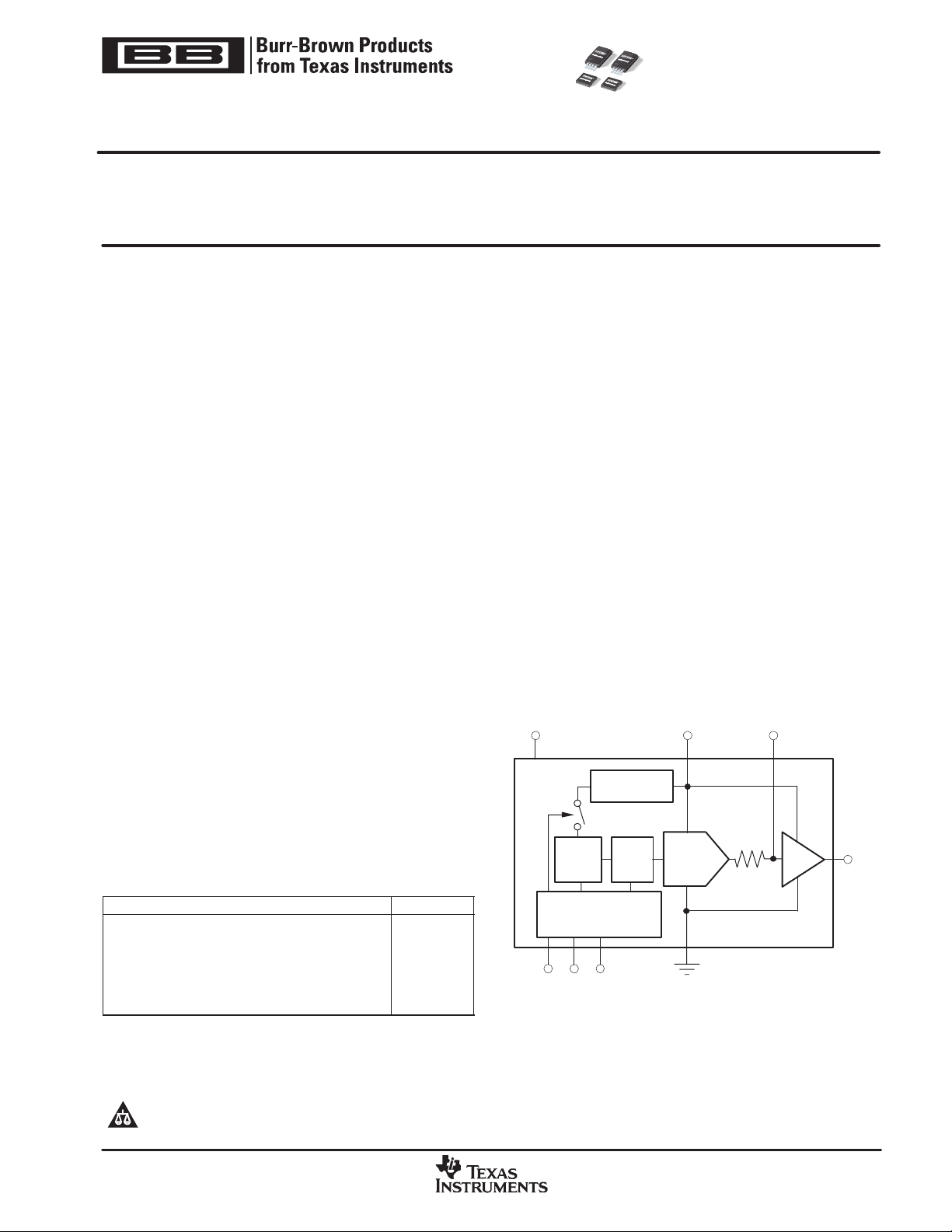
Programmable Voltage Source
with Memory
BUF01900
BUF01901
FEATURES
D 10-BIT RESOLUTION
D RAIL-TO-RAIL OUTPUT
D ONBOARD NONVOLATILE MEMORY
D I
OUT
: 100mA
D LOW SUPPLY CURRENT: 900µA
D SUPPLY VOLTAGE: 7V to 18V
D DIGITAL SUPPLY: 2.0V to 5.5V
D INDUSTRY-STANDARD, TWO-WIRE
INTERFACE
D HIGH ESD RATING:
2kV HBM, 500V CDM
APPLICATIONS
D LCD PANEL V
D LCD PANEL BRIGHTNESS AND CONTRAST
CONTROL
D POTENTIOMETER REPLACEMENT
D MOTOR DRIVE
D PROGRAMMABLE POWER SUPPLY
D PROGRAMMABLE OFFSET ADJUSTMENT
D ACTUATOR CONTROL
CALIBRATION
COM
DESCRIPTION
The BUF01900 and BUF01901 provide a programmable
voltage output with 10-bit resolution. Programming of the
output occurs through an industry-standard, two-wire
serial interface. Once the correct V
established it can easily be stored into the integrated
nonvolatile memory.
An initial output voltage and adjustment range can be set
by an external resistor-divider. With its large output current
capability (up to 100mA), the BUF01900 and BUF01901
are ideally suited as programmable V
LCD panels.
The BUF01901 has the digital-to-analog converter (DAC)
output brought out directly . It has a slightly lower cost than
the BUF01900, and works very well with the integrated
V
in traditional gamma buffers such as the BUFxx702,
COM
BUFxx703, BUFxx704 and BUF11705.
The BUF01900 and BUF01901 are both available in
TSSOP-8 and 3mm x 3mm DFN-10 packages. The
DFN-10 package (only 0.9mm in height) is especially
well-suited for notebook computers. Both devices are
specified from −40°C to +85°C.
Digital
2V to 5.5V
BUF01900
Voltage
Regulator
Analog
7V to 18V
voltage is
COM
calibrators in
COM
BIAS
250k
4xOTP
ROM
BUF01900, BUF01901 RELATED PRODUCTS
FEATURES PRODUCT
22V High Supply V oltage Gamma Buffers BUF11705
12--Channel Programmable Buffer, 10-Bit, V
20-Channel Programmable Buffer, 10-Bit, V
16-Channel Programmable Buffer with Memory BUF16820
20-Channel Programmable Buffer with Memory BUF20820
semiconductor products and disclaimers thereto appears at the end of this data sheet.
PowerPAD is a registered trademark of Texas Instruments. All other trademarks are the property of their respective owners.
! !
COM
COM
BUF12800
BUF20800
www.ti.com
Program Command
Input Control Logic
SDA
SCL A0
Switch
Control
10−Bit
DAC
Copyright 2006, Texas Instruments Incorporated
Ω
Buffer
V
COM
Page 2
"#$%&$$
"#$%&$%
SBOS337A − OCTOBER 2006 − REVISED OCTOBER 2006
This integrated circuit can be damaged by ESD. Texas Instruments recommends that all integrated circuits be handled with appropriate
precautions. Failure to observe proper handling and installation procedures can cause damage.
ESD damage can range from subtle performance degradation to complete device failure. Precision integrated circuits may be more
susceptible to damage because very small parametric changes could cause the device not to meet its published specifications.
www.ti.com
ABSOLUTE MAXIMUM RATINGS
(1)
Supply Voltage, VS +20V. . . . . . . . . . . . . . . . . . . . . . . . . . . . . . . . . . . . . . . . . . . . . . . . . . . . . . . . . . . . . . . . . . . . . . . . . . . . . . . . . . . . . . . . . . . . . . . . . .
Supply Voltage, VSD +6V. . . . . . . . . . . . . . . . . . . . . . . . . . . . . . . . . . . . . . . . . . . . . . . . . . . . . . . . . . . . . . . . . . . . . . . . . . . . . . . . . . . . . . . . . . . . . . . . . .
Signal Input Terminals,
BIAS:
Voltage −0.5V to VS +0.5V. . . . . . . . . . . . . . . . . . . . . . . . . . . . . . . . . . . . . . . . . . . . . . . . . . . . . . . . . . . . . . . . . . . . . . . . . . . . . . . . . . . . . . . . . . . . . . .
SCL, SDA, A0, A1:
Voltage −0.5V to +6V. . . . . . . . . . . . . . . . . . . . . . . . . . . . . . . . . . . . . . . . . . . . . . . . . . . . . . . . . . . . . . . . . . . . . . . . . . . . . . . . . . . . . . . . . . . . . . . . . . .
Current ±10mA. . . . . . . . . . . . . . . . . . . . . . . . . . . . . . . . . . . . . . . . . . . . . . . . . . . . . . . . . . . . . . . . . . . . . . . . . . . . . . . . . . . . . . . . . . . . . . . . . . . . . . . .
Output Short Circuit
(2)
Continuous. . . . . . . . . . . . . . . . . . . . . . . . . . . . . . . . . . . . . . . . . . . . . . . . . . . . . . . . . . . . . . . . . . . . . . . . . . . . . . . . . . . . . . . . . . .
Operating Temperature −40°C to +95°C. . . . . . . . . . . . . . . . . . . . . . . . . . . . . . . . . . . . . . . . . . . . . . . . . . . . . . . . . . . . . . . . . . . . . . . . . . . . . . . . . . . . . .
Storage Temperature −65°C to +150°C. . . . . . . . . . . . . . . . . . . . . . . . . . . . . . . . . . . . . . . . . . . . . . . . . . . . . . . . . . . . . . . . . . . . . . . . . . . . . . . . . . . . . . .
Junction Temperature +125°C. . . . . . . . . . . . . . . . . . . . . . . . . . . . . . . . . . . . . . . . . . . . . . . . . . . . . . . . . . . . . . . . . . . . . . . . . . . . . . . . . . . . . . . . . . . . . . .
ESD Rating:
Human Body Model (HBM) 2000V. . . . . . . . . . . . . . . . . . . . . . . . . . . . . . . . . . . . . . . . . . . . . . . . . . . . . . . . . . . . . . . . . . . . . . . . . . . . . . . . . . . . . . . .
Charged-Device Model (CDM) 500V. . . . . . . . . . . . . . . . . . . . . . . . . . . . . . . . . . . . . . . . . . . . . . . . . . . . . . . . . . . . . . . . . . . . . . . . . . . . . . . . . . . . . .
(1)
Stresses above these ratings may cause permanent damage. Exposure to absolute maximum conditions for extended periods may degrade
device reliability. These are stress ratings only, and functional operation of the device at these or any other conditions beyond those specified is
not supported.
(2)
Short-circuit to ground.
ORDERING INFORMATION
(1)
PRODUCT PACKAGE-LEAD PACKAGE DESIGNATOR PACKAGE MARKING
BUF01900 DFN-10 DRC BOO
BUF01900 TSSOP-8 PW F01900
BUF01901 DFN-10 DRC BOP
BUF01901 TSSOP-8 PW F01901
(1)
For the most current package and ordering information, see the Package Option Addendum at the end of this document, or see the TI web site
at www .ti.com.
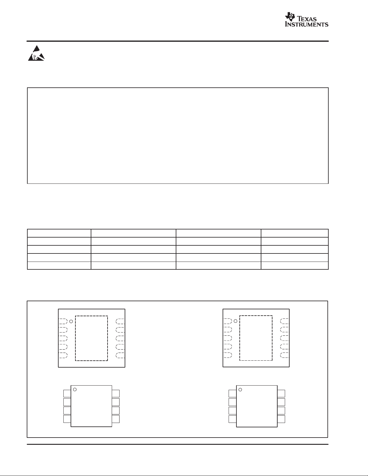
PIN CONFIGURATIONS
BUF01900
1
V
S
2
V
COM
3
BIAS
4
GND
5
DGND
V
1
S
V
2
COM
3
BIAS
4
GND
2
Exposed
Thermal
Die Pad
on
Underside
DFN−10
BUF01900
TSSOP−8
BUF01901
SDA
10
9
SCL
8
A0
7
A1
6
V
SD
8
SDA
7
SCL
6
A0
V
5
SD
NC
BIAS
GND
DGND
V
S
NC
BIAS
GND
1
2
3
4
5
V
S
Exposed
Thermal
Die Pad
on
Underside
DFN−10
BUF01901
1
2
3
4
TSSOP−8
SDA
10
SCL
9
A0
8
A1
7
V
6
SD
SDA
8
SCL
7
6
A0
5
V
SD
NC = No connection
Page 3

"#$%&$$
"#$%&$%
www.ti.com
SBOS337A − OCTOBER 2006 − REVISED OCTOBER 2006
ELECTRICAL CHARACTERISTICS
Boldface limits apply over the specified temperature range, TA = −40°C to +85°C.
At TA = +25°C, VS = 18V, VSD = 5V, RL = 1.5kΩ connected to ground, and CL = 200pF, unless otherwise noted.
PARAMETER CONDITIONS MIN TYP MAX UNIT
ANALOG
V
Output Swing
COM
(1)
Sourcing 10mA, Code 1023 17.7 17.8 V
Sinking 10mA, Code 00 0.6 1 V
Sourcing 100mA, Code 1023 15 16 V
Sinking 100mA, Code 00 0.75 1 V
V
Output Reset and Power-Up Value
COM
Nominal V
Program to Out Delay t
Output Impedance No Load on V
BIAS
(1)
D
OTP not programmed, Code 512 VS/2 V
Output Accuracy 1V < V
Load Regulation REG V
(1)
V
COM
OUT
= VS/2, I
Offset ±5 ±25 mV
Offset Drift −25°C to +100°C 5 µV/°C
Common-Mode Range 0.8 to 18 V
Common-Mode Rejection CMR 0.8V < VIN < 17.9V 85 dB
Slew Rate 5 V/µs
V
BIAS
Integral Nonlinearity INL 0.1 2 LSB
Differential Nonlinearity DNL 0.1 2 LSB
Gain Error 0.1 1 %FSC
Accuracy 20 50 mV
ANALOG POWER SUPPLY
Operating Range
Total Analog Supply Current I
(2)
V
S
S
Output at Reset Values, No Load 0.9 1.5 mA
over Temperature 1.5 mA
DIGITAL
Logic 1 Input Voltage V
Logic 0 Input Voltage V
Logic 0 Output Voltage V
IH
IL
OL
Input Leakage ±0.01 ±10 µA
Clock Frequency f
CLK
Standard/Fast Mode 400 kHz
DIGITAL POWER SUPPLY
Operating Voltage Range V
Digital Supply Current
(2)
SD
I
SD
over Temperature 100 µA
TEMPERATURE
Specified Temperature Range −40 +85 °C
Operating Temperature Range Junction Temperature < 125°C −40 +95 °C
Storage Temperature Range −65 +150 °C
Thermal Resistance q
JA
TSSOP-8 150 °C/W
DFN-10 47 °C/W
(1)
BUF01900 only.
(2)
Minimum analog supply voltage is 8.5V when programming OTP memory.
BUF01900, BUF01901
BIAS
, V
COM
250 kΩ
5 µs
< 17.7 20 50 mV
COM
= +50mA to −50mA Step 0.5 1.5 mV/mA
OUT
No Load on V
BIAS
7 18 V
0.7 × V
SD
I
= 3mA 0.15 0.4 V
SINK
0.3 × V
SD
High-Speed Mode 3.4 MHz
2.0 5.5 V
25 50 µA
V
V
3
Page 4

"#$%&$$
"#$%&$%
SBOS337A − OCTOBER 2006 − REVISED OCTOBER 2006
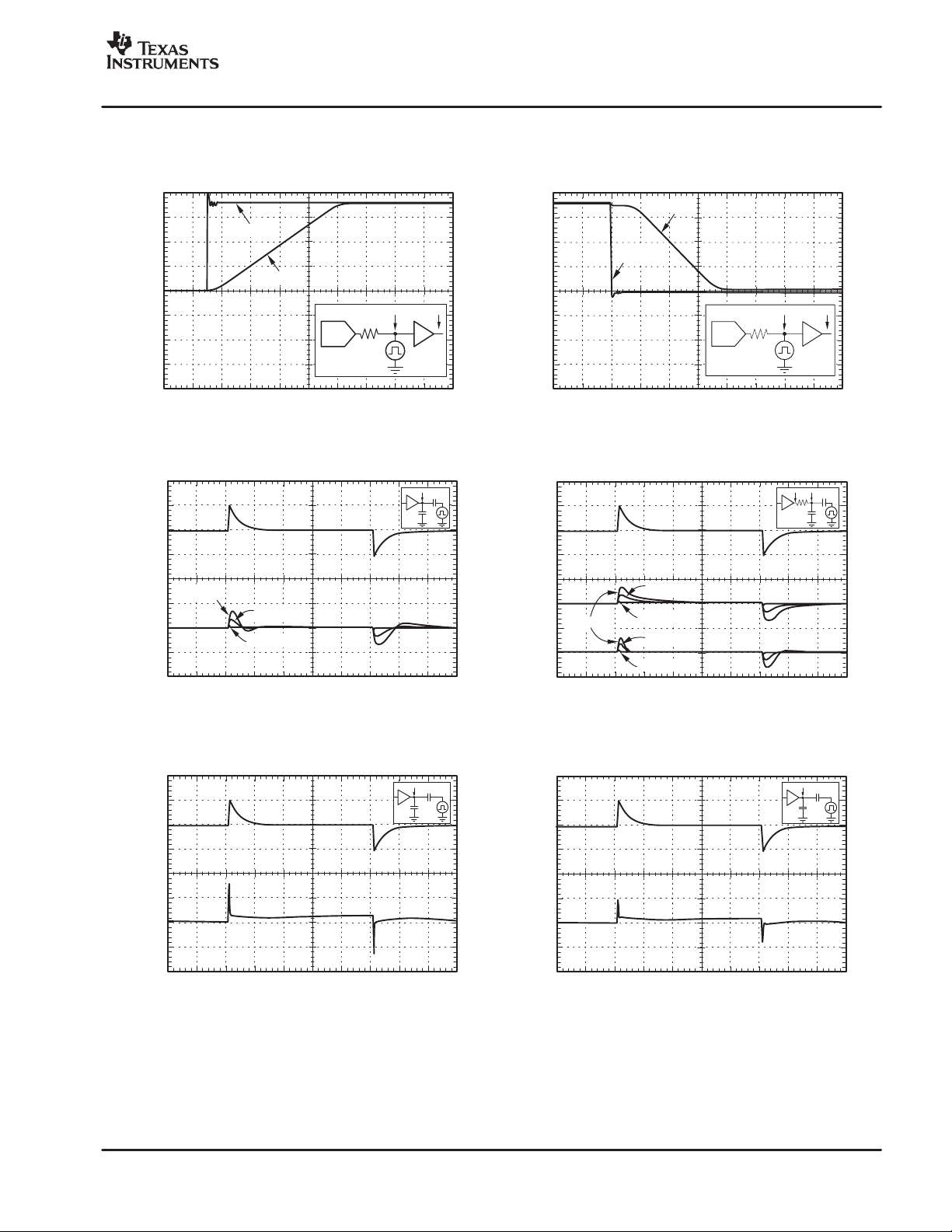
TYPICAL CHARACTERISTICS
At TA = +25°C, VS = 18V , VSD = 5V , RL = 1.5kΩ connected to ground, and CL = 200pF, unless otherwise noted.
www.ti.com
1.5
1.0
0.5
Analog Supply Current (mA)
(mV)
OS
V
−10
−15
−20
−
ANALOG SUPPLY CURRENT vs TEMPERATURE
V
VSD=8V
0
−
40−20 0 10040 60 8020
BUFFEROFFSET VOLTAGEvs TEMPERAT U RE
25
PDS limits are ±25mV
20
15
10
5
0
−5
25
−40 −20 0 10040 60 8020
S
= 18V
(V
Temperature (_C)
Figure 1
=18V,VSD=5V)
S
Temperature (_ C)
Figure 3
50
A)
40
µ
30
20
10
Digital Supply Current (
DIGITA LSUPPLY CURRENT vs TEMPERATURE
VSD=5V
VSD=2V
0
−
40−20 0 10040 60 8020
Temperature (_C)
Figure 2
20
18
16
14
12
(V)
10
OUT
V
8
6
4
2
0
OUTPUT VOLTAGEvs OUTPUT CURRENT
V
= 18V
S
Sourcing, Code = 3FFh
Sinking, Code = 000h
0 25 10050 75
(mA)
I
OUT
Figure 4
INTEGRAL NONLINEARITY ERROR vs INPUT CODE
1.5
1.0
0.5
0
−
INL Error(L SB)
0.5
−
1.0
10 Typical Units Shown
−
1.5
0 128 256 384 512 1024
Input Code
640 768 896
Figure 5
1.5
1.0
0.5
0
−
0.5
DNL Error (LSB)
−
1.0
−
1.5
0 128 256 384 512 1024
DIFFERENTIAL NONLINEARITY ERROR
vs INPUT CODE
10 Typical Units Shown
640 768 896
Input Decimal Code
Figure 6
4
Page 5
www.ti.com
SBOS337A − OCTOBER 2006 − REVISED OCTOBER 2006
TYPICAL CHARACTERISTICS (cont)
At TA = +25°C, VS = 18V , VSD = 5V , RL = 1.5kΩ connected to ground, and CL = 200pF, unless otherwise noted.
V
BUFFER SLEW RATE
COM
(1) V
BIAS
(2) V
COM
5V/div
1 2
5V/div
BUFFER LARGE SIGNAL STEP RESPONSE
(2) V
COM
(1) V
BIAS
"#$%&$$
"#$%&$%
1 2
100mA/div500mV/div
1
Time (1µs/div)
Figure 7
LOAD REGULATION vs CAPACITANCE
C=0.1µF
C=1µF
C=10µF
Time (1µs/div)
Figure 9
LOAD REGULATION WITH 100µF CAPACITOR
Time (1µs/div)
Figure 8
LOAD REGULATION vs CAPACITANCE
1
2.7nF
C
1
2
Ω
2.7nF
10
C
100mA/div500mV/div
C=1µF
2
C=0.1µF
C=10µF
C=1µF
1
C=10µF
Time (1µs/div)
Figure 10
LOAD REGULATION WITH 10µFCAPACITOR
1
2.7nF
100µF
1
2.7nF
10µF
1
20mV/div 100mA/div
Time (1µs/div)
Figure 11
1
50mV/div 100mA/div
Time (1µs/div)
Figure 12
5
Page 6
"#$%&$$
"#$%&$%
SBOS337A − OCTOBER 2006 − REVISED OCTOBER 2006
TYPICAL CHARACTERISTICS (cont)
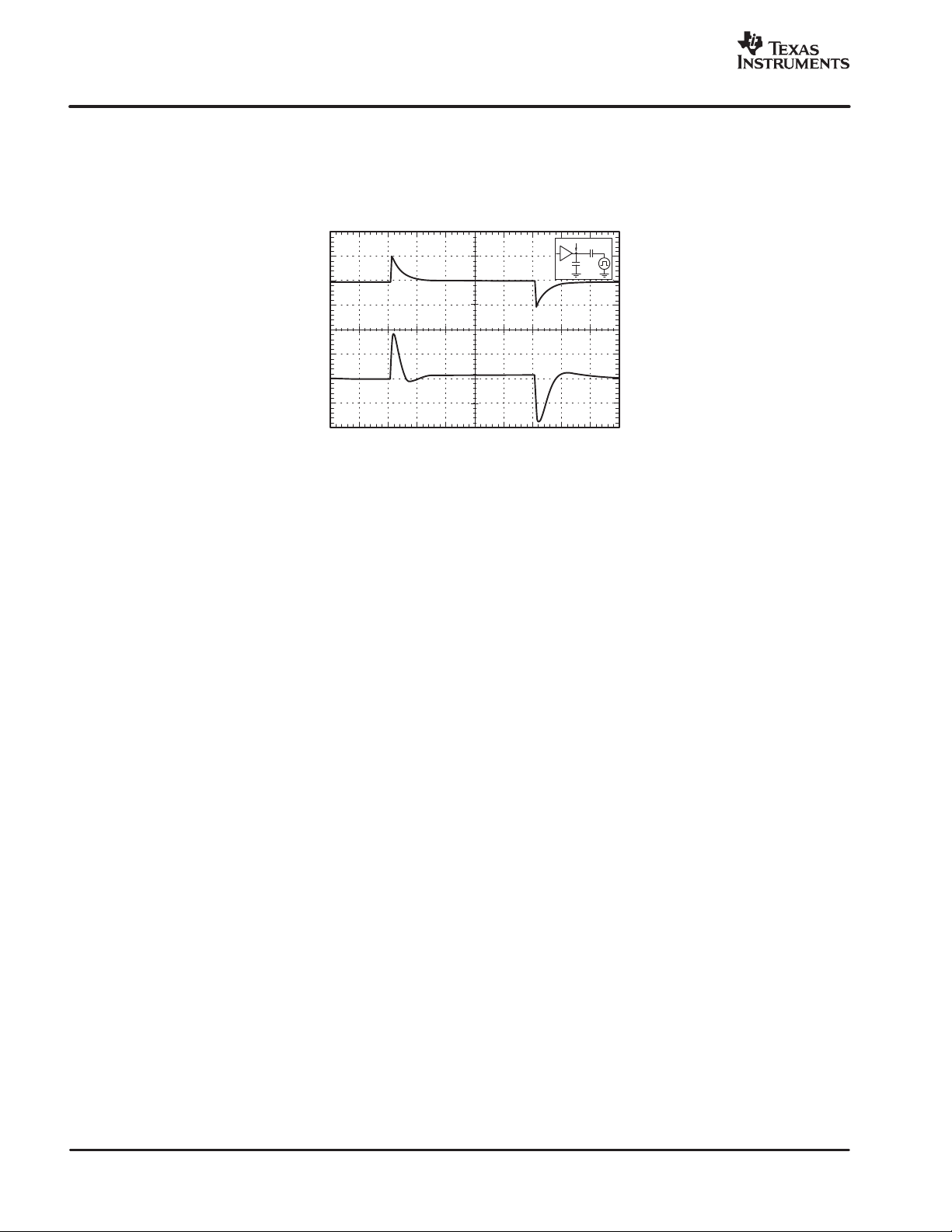
At TA = +25°C, VS = 18V , VSD = 5V , RL = 1.5kΩ connected to ground, and CL = 200pF, unless otherwise noted.
www.ti.com
LOAD REGULATION WITH 1µFCAPACITOR
(C = 1µF, R
1
100mV/div 100mA/div
=0,100mVRes.)
S
Time (1µs/div)
1
2.7nF
1µF
Figure 13
6
Page 7
www.ti.com
"#$%&$$
"#$%&$%
SBOS337A − OCTOBER 2006 − REVISED OCTOBER 2006
APPLICATIONS INFORMATION
OVERVIEW
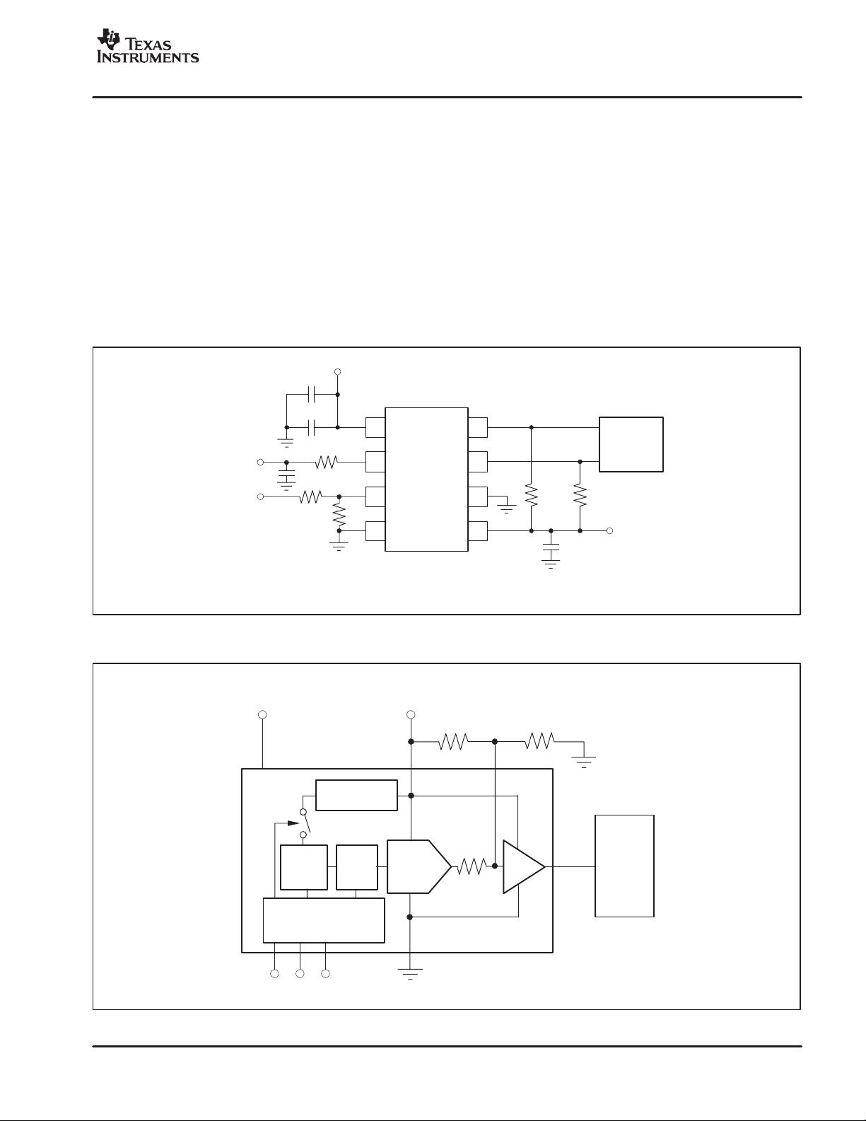
The BUF0190x family of products consists of a 10-bit digital-to-analog converter (DAC) that is programmed through
an industry-standard two-wire interface. It contains onchip nonvolatile memory that stores a specific DAC value
that is read at power-up. The BUF0190x family consists of
two devices: The BUF01900 contains a voltage buffer that
is capable of driving high-current; the BUF01901 is a lower-cost version without the buffer. The BUF0190x is especially well-suited for V
ever, it can also be used in many other applications.
Figure 14 shows the BUF01900 in a typical configuration.
calibration in LCD panels; how-
COM
V
S
0.1µF
10µF
+
V
COM
V
S
(1)
(2)
(2)
1
2
3
4
BUF01900
V
S
V
COM
V
BIAS
GND
BUF01900: ON-CHIP BUFFER
Unlike many programmable V
ket, the BUF01900 offers an integrated V
high current output drive capability. The output is capable
of delivering peak currents over 100mA to within 4V from
the positive supply and to within 2V from the negative supply. Using this option is very cost-ef fective and convenient
in systems that do not use multi-channel gamma buffers
with integrated V
drive. Figure 15 shows the
COM
BUF01900 in a typical configuration.
SDA
SCL
V
8
7
Ω
A
6
0
5
SD
10k
0.1µF
10k
Timing
Controller
Ω
V
calibrators on the mar-
COM
SD
buffer with
COM
Digital
2V to 5.5V
BUF01900
Program Command
SDA
(1) Optional −may be needed for stability.
NOTES:
(2) Optional −see application text for component selection.
Figure 14. Typical Application Diagram
Analog
7V to 18V
R
1
BIAS
Voltage
Regulator
Ω
4xOTP
ROM
Input Control Logic
SCL A0
Switch
Control
10−Bit
DAC
250k
V
COM
Buffer
R
2
V
COM
Panel
Figure 15. BUF01900 Typical Configuration
7
Page 8
"#$%&$$
"#$%&$%
SBOS337A − OCTOBER 2006 − REVISED OCTOBER 2006
www.ti.com
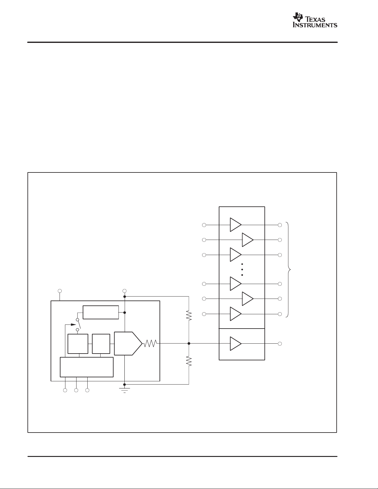
BUF01901: USING EXTERNAL V
COM
BUFFER
Many LCD panel modules use gamma buffers, such as
TI’s BUFxx704, BUFxx703, BUF11702 and the new
BUF11705, that already include an integrated V
COM
driver.
Some other LCD modules use more complicated compensation schemes that require an external high-speed
V
op amp. BUF01901 is optimized for lowest cost and
COM
is intended to be used with an external V
buffer or op
COM
amp. Figure 16 illustrates a typical configuration of the
BUF01901 with the BUF11705.
ON-CHIP NONVOLATILE MEMORY
The BUF0190x is optimized for the smallest die size available and consequently the lowest cost to support high vol-
ume production. The on-chip OTP (one-time-programmable) memory helps to achieve significant die size
reduction over EEPROM memory technology . This reduction is partly because of the smaller area of the OTP
memory cell, but also a result of the fact that an EEPROM
requires a high programming voltage typically generated
with an onboard charge pump. OTP memory technology
does not require the higher programming voltage; consequently, no charge pump is needed, resulting in a smaller
and lower-cost solution.
During production, the V
voltage is typically adjusted
COM
only once. However, to allow for programming errors and
rework, the BUF0190x supports a total of four write cycles
to the OTP memory. This capacity means that the previously programmed code in the OTP can be overwritten
a total of three times.
BUF11704
Digital
2V to 5.5V
BUF01901
Program Command
SDA
Voltage
Regulator
4xOTP
ROM
Input Control Logic
SCL A0
Switch
Control
Analog
7V to 18V
R
1
Ω
250k
10−Bit
DAC
BIAS
R
2
Figure 16. BUF01901 Typical Configuration
V
COM
Gamma
References
8
Page 9

www.ti.com
"#$%&$$
"#$%&$%
SBOS337A − OCTOBER 2006 − REVISED OCTOBER 2006
POWER-SUPPLY VOLTAGE
The BUF0190x can be powered using an analog supply
voltage from 7V to 18V, and a digital supply from 2V to
5.5V. The digital supply must be applied prior to the analog
supply to avoid excessive current and power consumption.
During programming of the OTP, the analog power supply
must be at least 8.5V.
BUFFER INPUT AND OUTPUT RANGE
The integrated buffer has a single p-channel input stage.
The input range includes the positive supply and extends
down to typically 0.8V above the negative supply (GND).
In a typical LCD application, this is normally sufficient because the nominal V
level is often close to V2/2 and,
COM
therefore, fairly far away from either supply rail. In addition,
the adjustment range is usually not much larger than 1V in
either direction of the nominal V
voltage. In applica-
COM
tions requiring a wider output swing, the output voltage to
the buffer should be limited to approximately 0.8V above
the negative power supply to keep the buffer input stage
in its linear operating region. For lower input voltages, the
output results might not be valid; however, they will also
not lead to damage of the device.
The Rail-to-Rail output stage is designed to drive large
peak currents greater than 100mA.
TWO-WIRE BUS OVERVIEW
The BUF0190x communicates through an industry-standard, two-wire interface to receive data in slave mode. This
standard uses a two-wire, open-drain interface that supports multiple devices on a single bus. Bus lines are driven
to a logic low level only . The device that initiates the communication is called a master, and the devices controlled
by the master are slaves. The master generates the serial
clock on the clock signal line (SCL), controls the bus access, and generates START and STOP conditions.
To address a specific device, the master initiates a START
condition by pulling the data signal line (SDA) from a HIGH
to LOW logic level while SCL is HIGH. All slaves on the bus
shift in the slave address byte, with the last bit indicating
whether a read or write operation is intended. During the
ninth clock pulse, the slave being addressed responds to
the master by generating an Acknowledge and pulling
SDA LOW.
Data transfer is then initiated and eight bits of data are
sent, followed by an Acknowledge bit. During data transfer, SDA must remain stable while SCL is HIGH. Any
change in SDA while SCL is HIGH will be interpreted as a
START or STOP condition.
Once all data has been transferred, the master generates
a STOP condition, indicated by pulling SDA from LOW to
HIGH while SCL is HIGH.
The BUF0190x can act only as a slave device; therefore,
it never drives SCL. The SCL is only an input for the
BUF0190x.
ADDRESSING THE BUF01900 AND
BUF01901
The address of the BUF0190x in the TSSOP-8 package
is 111011x, where x is the state of the A0 pin. When the
A0 pin is LOW, the device acknowledges on address 76h.
If the A0 pin is HIGH, the device acknowledges on address
77h. Table 1 summarizes device addresses.
Table 1. Quick-Reference Table of Addresses
DEVICE/COMPONENT ADDRESS
TSSOP Package:
A0 pin is LOW
(device will acknowledge on address 76h)
A0 pin is HIGH
(device will acknowledge on address 77h)
DFN Package:
A0 pin is LOW, A1 is LOW
(device will acknowledge on address 74h)
A0 pin is HIGH, A1 is LOW
(device will acknowledge on address 75h)
A0 pin is LOW, A1 is HIGH
(device will acknowledge on address 76h)
A0 pin is HIGH, A1 is HIGH
(device will acknowledge on address 77h)
The address of the BUF0190x in the DFN-10 package is
11101yx, where x is the state of the A0 pin and y is the state
of the A1 pin. When the A0 and A1 pins are both LOW, the
device acknowledges on address 74h. If the A0 is HIGH
and A1 is L O W, the device acknowledges on address 75h.
When the A0 is LOW, and A1 is HIGH, the device acknowledges on address 76h. If the A0 and A1 pins are both
HIGH, the device address is 77h.
Other addresses are possible through a simple mask
change. Contact your TI representative for ordering information and availability.
1110110
1110111
1110100
1110101
1110110
1110111
9
Page 10

"#$%&$$
"#$%&$%
SBOS337A − OCTOBER 2006 − REVISED OCTOBER 2006
www.ti.com
DATA RATES
The two-wire bus operates in one of three speed modes:
D Standard: allows a clock frequency of up to 100kHz;
D Fast: allows a clock frequency of up to 400kHz; and
D High-speed mode (or Hs mode): allows a clock
frequency of up to 3.4MHz.
The BUF0190x is fully compatible with all three modes. No
special action is required to use the device in Standard or
Fast modes, but High-speed mode must be activated. To
activate High-speed mode, send a special address byte of
00001xxx, with SCL ≤ 400kHz, following the ST ART condition; xxx are bits unique to the Hs-capable master, which
can be any value. This byte is called the Hs master code.
(Note that this is different from normal address bytes—the
low bit does not indicate read/write status.) The BUF0190x
will respond to the High-speed command regardless of t h e
value of these last three bits. The BUF0190x does not acknowledge this byte; the communication protocol prohibits
acknowledgment of the Hs master code. On receiving a
master code, the BUF0190x switches on its Hs mode filters, and communicates at up to 3.4MHz.
Additional high-speed transfers may be initiated without
resending the Hs mode byte by generating a repeat
START without a STOP. The BUF0190x switches out of Hs
mode with the next STOP condition.
GENERAL CALL RESET AND POWER-UP
The BUF0190x responds to a General Call Reset, which
is an address byte of 00h (0000 0000) followed by a
data byte of 06h (0000 0110). The BUF0190x acknowledges both bytes. Upon receiving a General Call Reset,
the BUF0190x performs a full internal reset, as though it
had been powered off and then on. It always acknowledges the General Call address byte of
00h (0000 0000), but does not acknowledge any General
Call data bytes other than 06h (0000 0110).
The BUF0190x automatically performs a reset upon power-up. As part of the reset, the BUF0190x is configured for
the output to change to the programmed OTP memory value, or to mid-scale, ‘1000000000’, if the OTP value has not
been programmed. Table 2 provides a summary of command codes.
READ/WRITE OPERATIONS:
Read commands are performed by setting the read/write
bit HIGH. Setting the read/write bit LOW performs a write
transaction.
Figure 17 and Figure 18 show the timing diagrams for read
and write operations.
Writing:
To write to the DAC register:
1. Send a START condition on the bus.
2. Send the device address and read/write bit = LOW.
The BUF01900/BUF01901 will acknowledge this
byte.
3. Send two bytes of data for the DAC register. Begin by
sending the most significant byte (bits D15—D8; only
bits D9 and D8 are used, and D15—D13 must not be
010 or 001), followed by the least significant byte (bits
D7—D0). The register is updated after receiving the
second byte.
4. Send a STOP condition on the bus.
The BUF0190x acknowledges each data byte. If the master terminates communication early by sending a STOP or
START condition on the bus, the DAC output will not update.
Reading:
To read the register of the DAC:
1. Send a START condition on the bus.
2. Send the device address and read/write bit = HIGH.
The BUF0190x will acknowledge this byte.
3. Receive two bytes of data. The first received byte is
the most significant byte (bits D15—D8; only bits D9
and D8 have meaning, and bits D15—D12 will show
the programming status of the OTP memory). See
Table 3. The next byte is the least significant byte (bits
D7—D0).
4. Acknowledge after receiving the first byte only.
5. Do not acknowledge the second byte of data or send
a STOP condition on the bus.
Communication may be terminated by the master by
sending a premature STOP or START condition on the
bus, or by not sending the Acknowledge.
Table 2. Quick-Reference Table of Command
Codes
COMMAND CODE
General Call Reset
High-Speed Mode
10
Address byte of 00h followed by a data byte
of 06h.
00001xxx, with SCL ≤ 400kHz; where xxx
are bits unique to the Hs-capable master.
This byte is called the Hs master code.
Table 3. OTP Memory Status
CODE
(Bits D15 − D12)
0000 OTP has not been programmed.
0001 OPT has been programmed once.
0011 OTP has programmed twice.
0111 OPT has programmed three times.
1111 OTP has programmed all four times.
OTP PROGRAMMING STATUS
Page 11

www.ti.com
"#$%&$$
"#$%&$%
SBOS337A − OCTOBER 2006 − REVISED OCTOBER 2006
ACQUIRE OF OTP MEMORY
An acquire command updates the DAC output to the value
stored in OTP memory. If the OTP memory has not been
programmed, the DAC output code is ‘0000000000’.
Figure 19 shows the timing diagram for the acquire
command.
Acquire Command
1. Send a START condition on the bus.
Send the device address and read/write bit = LOW .
2.
The device will acknowledge this byte.
3. Send the acquire command. Bits D7—D5 must be
set to 001. Bits D4—D0 do not have meaning. This
byte will be acknowledged.
4. Send a STOP condition on the bus.
Writing OTP Memory
The BUF0190x is able to write to the OTP memory a maximum of four times. Writing to the OTP memory a fourth
time uses all available memory and disables the ability to
perform additional writes (see table 3). A reset or acquire
command updates the DAC output to the most recently
written OTP memory value.
When programming the OTP memory, the analog supply
voltage must be between 8.5V and 18V.
Write commands are performed by setting the read/write
bit LOW.
To write to OTP memory:
1. Send a START condition on the bus.
2. Send the device address and read/write bit = LOW.
The BUF0190x acknowledges this byte.
3. Send two bytes of data for the OTP memory. Begin by
sending the most significant byte first (bits D15
of which only bits D9 and D8 are data bits, and bits
D15
—D13 must be 010), followed by the least
significant byte (bits D7
after receiving the second byte.
4. Send a STOP condition on the bus.
The BUF0190x acknowledges each data byte. If the master terminates communication early by sending a STOP or
START condition on the bus, the specified OTP register
will not be updated. Writing an OTP register updates the
DAC output voltage.
Programming timing is taken from the two-wire bus.
Therefore, the master must provide correct timing on the
bus to ensure data is successfully written into OTP
memory. Figure 20 shows the timing requirements for timing when the OTP write supply and OTP write signal are
active.
—D0). The register updates
—D8,
11
Page 12

"#$%&$$
"#$%&$%
SBOS337A − OCTOBER 2006 − REVISED OCTOBER 2006
isupdated in thismoment.
The entire DAC Register D9 −D0
www.ti.com
DACLSbyt e . Ackn Stop
Ackn D7 D6 D5 D4 D3 D2 D1 D0 Ackn
Ackn D7 D6 D5 D4 D3 D2 D1 D0 Ackn
DACLSbyte. NoAckn Stop
Ackn D7 D6 D5 D4 D3 D2 D1 D0
Ackn D7 D6 D5 D4 D3 D2 D1 D0 No Ackn
0000 OTPhas not been programmed
0001 OTPhas been programmedonce
001 1 OTP has beenprogrammedtwice.
01 11 OTP has beenprogrammedthree times.
1 111 OTP has beenprogrammedfour times.
CODE OTPProgrammingStatus
Write DAC Register. Write operation
Start Deviceaddress Write A ck n DACMSbyte. D15 −D13 = ’000’D 12−D10 have no meanin g. Ackn
SCL
SDA_in A 6 A5 A4 A3 A2 A1 A0 W Ackn D15 D14 D13 D12 D11 D10 D9 D8
Device_out A6A5A4A3A2A1A0WAcknD15D14D13D12D11D10D9D8
Figure 17. Timing Diagram for Write DAC Register
12
Read DAC Register. Readoperation
Start Deviceaddress Write Ackn DAC MSbyte.D15 −D12 showthe program status. A c kn
SCL
SDA_in A6 A5 A4 A3 A2 A1 A0 R Ackn D15 D14 D13 D12 D11 D10 D9 D8
Device_out A6 A5 A4 A3 A2 A1 A0 R Ackn D15 D14 D13 D12 D11 D10 D9 D8
Figure 18. Timing Diagram for Read DAC Register
Page 13

www.ti.com
"#$%&$$
"#$%&$%
SBOS337A − OCTOBER 2006 − REVISED OCTOBER 2006
2
t
1
t
Write supply active
DAC output is
updated in this moment.
s, maximum 2ms.
µ
sbefore falling edge of clock.
µ
:>20
: minimum100
is updated in thismoment.
1
2
The OTP Register D9 −D0
t
t
Acquire command. Write operation
Start Device address Write Ackn D15−D13 must be ’001’. D12 −D8 have no meaning. Ackn Stop
SCL
SDA_in A6 A5 A4 A3 A2 A1 A0 W Ackn D7 D6 D5 D4 D3 D2 D1 D0 Ackn
Device_out A6 A5 A4 A3 A2 A1 A0 W Ackn D15 D14 D13 D12 D11 D10 D9 D8 Ackn
Figure 19. Timing Diagram for Acquire Command
Write OTPmemory. Writeoperation W r itesignalactive
Start Device address Write Ackn DAC MSbyte. D15 −D13 must be 010. D12 −D10 have no meaning. Ackn DAC LSbyte. Ackn Stop
SCL
SDA_in A6 A5 A4 A3 A2 A1 A0 W Ackn D15 D14 D13 D12 D11 D10 D9 D8 Ackn D7 D6 D5 D4 D3 D2 D1 D0 Ackn
Device_out A6 A5 A4 A3 A2 A1 A0 W Ackn D15 D14 D13 D12 D11 D10 D9 D8 Ackn D7 D6 D5 D4 D3 D2 D1 D0 Ackn
Figure 20. Timing Diagram for Write OTP Register
13
Page 14

"#$%&$$
"#$%&$%
SBOS337A − OCTOBER 2006 − REVISED OCTOBER 2006
www.ti.com
V
CALIBRATION
COM
The BUF0190x provides a simple, time- and cost-efficient
means to adjust the flicker performance of LCD panels either manually or automatically during the final stages of the
LCD panel manufacturing process.
The 10-bit adjustment resolution of the BUF0190x exceeds the typical adjustment resolution of existing V
calibrators significantly. As with a traditional V
COM
COM
adjustment, which uses a mechanical potentiometer and a voltage divider for adjustment (see Figure 21), the BUF0190x
uses an external voltage divider that is used to set the initial V
voltage as well as the adjustment range.
COM
AVDD
R
A
R
B
R
C
V
COM
(a) Code 00h equivalent circuit.
BUF0190x
250k
(b) Code 3FFh equivalent circuit.
BUF0190x
V
S
250k
V
S
R
1
Ω
Ω
R
2
V
S
R
1
R
2
(1)
V
V
BIAS
V
BIAS
COM
(1)
V
COM
Figure 21. Traditional V
Adjustment
COM
As Figure 22 shows, the 10-bit DAC acts as a Rail-to-Rail
output voltage source with a nominal 250kΩ of output impedance. For example, at Code 000h, the lowest V
COM
voltage is achieved since the 250kΩ impedance is now in
parallel with R
, which lowers the impedance of the lower
2
side of the voltage divider. Consequently, code 3FFh results in the highest adjustable V
COM
voltage.
Once the desired output level is obtained, the part can
store the final setting using the non-volatile on-chip
memory. See Programming section for detailed information.
NOTE: (1) Integrated into BUF01900 or external.
Figure 22. Simplified Block Diagram for V
Adjustment using BUF0190x
COM
SELECTING THE ADJUSTMENT STEP SIZE
A maximum of 1024 adjustment steps can be realized with
the BUF0190x, leading to very high adjustment resolution
and very small step sizes. This flexibility can be advantageous during the panel development phase. In a practical
production setting, however, this capability might lead to
adjustment times that can be too long. A simple solution is
to increase the step size between settings to more practical values for mass production. Limiting the number of adjustment steps between code 000h and code 3FFh to between 16 and 128 has been shown to typically yield
acceptable adjustment results in the smallest amount of
adjustment time.
14
Page 15

www.ti.com
"#$%&$$
"#$%&$%
SBOS337A − OCTOBER 2006 − REVISED OCTOBER 2006
EXTERNAL VOLTAGE DIVIDER RESISTOR
SELECTION
The external resistive voltage-divider consisting of R1 and
R
(see Figure 16, Figure 17, and Figure 18) sets both the
2
maximum value of the V
tial V
correct values for R
voltage. Follow the steps below to calculate the
COM
1
Step 1: Choose the supply voltage, (V
Step 2: Set the nominal V
V
voltage at which the unadjusted panel should be at
COM
power-on. The default power-up DAC code is midscale.
Step 3: Choose the V
ment range is the difference between the lowest and the
highest desired V
COM
is not overwritten by software at the beginning of the adjustment cycle, the adjustment range is symmetrical
around the chosen nominal V
Step 4: Calculate the resistors based on the following formulas or simply download the Microsoft Excel calculator
located in the product folder of BUF0190x available at
www.ti.com.
R
1
R
2
250kW @ Adj_range
+
V
COM
+
V
S
V
COM
adjustment range and the ini-
COM
and R
2
voltage. This voltage is the
COM
adjustment range. The adjust-
COM
S)
voltage. If the default power-up code
voltage.
COM
* 0.5 @ (Adj_range)
(1)
1
1
ǒ
1
)
R
500kW
1
1
Ǔ
*
1
*
R
250kW
1
(2)
DESIGN EXAMPLE
Step 1: Supply Voltage is 10V.
Step 2: Nominal V
is determined to be 4V.
COM
Step 3: The desired total adjustment range is 1V. In the
case of using the default power-up DAC code (midscale),
the adjustment range for the V
voltage will be from
COM
3.5V to 4.5V.
Step 4: Calculation of R
and R
1
2
R1 = 71.4kΩ => choose closest 1% resistor (71.5kΩ)
R
= 45.5kΩ => choose closest 1% resistor (45.3kΩ)
2
Step 5: Appropriate number of adjustment steps between
code 00h and code 3FFh is determined to be 32. This value
leads to a step size of 32 codes between adjustment
points, which translates into approximately 31mV voltage
difference between steps.
MOTOR DRIVE CIRCUIT
The BUF01900 can be used to drive small motors directly
because of the large output drive capability (> 100mA), as
illustrated in Figure 23.
V
SD
15V
CALCULATING THE V
With R1 and R2 properly set, V
OUTPUT VOLTAGE
COM
BIAS
or V
output voltage
COM
can be calculated for any digital code with the following formula:
COM
250kW @ R
+
V
@ V
) R
2
@ R
R
1
2
@ R2@ V
1
S
) 250kW @ǒR1) R
(Codeń1023)
S
Ǔ
2
(3)
CALCULATING THE ADJUSTMENT
RESOLUTION
The resolution of the adjustment is a function of the step
size. The resolution can be calculated by simply dividing
the chosen adjustment range by the number of steps:
Resolution = Adj_range/steps (example: 32 steps between code 0h and code 3FFh)
10kΩ 10kΩ
µC
Figure 23. Motor Drive Circuit
BUF01900
V
COM
M
15
Page 16

"#$%&$$
"#$%&$%
SBOS337A − OCTOBER 2006 − REVISED OCTOBER 2006
www.ti.com
PROGRAMMABLE POWER SUPPLY
The BUF0190x integrated buffer amplifier can drive large
capacitive loads (see Typical Characteristics) and greater
than 100mA of output current, making it well-suited for programmable power supplies.
Note that the BUF01900 integrated buffer has an input
range that only extends to about 0.8V above GND; therefore, the programmable power supply is not able to output
voltages less than approximately 0.8V.
3.3V
Ω
10k
µ
C
NOTE: (1) Optional −see Typical Characteristic curves
Ω
10k
Figure 10 through Figure 14 for load regulation
performance.
15V
BUF01900
(1)
+
Load
100µF
QFN/DFN THERMALLY-ENHANCED
PACKAGE
The BUF0190x uses the 10-lead DFN package, a thin,
thermally-enhanced package designed to eliminate the
use of bulky heat sinks and slugs traditionally used in thermal packages. The DFN package can be easily mounted
using standard printed circuit board (PCB) assembly techniques. See QFN/SON PCB Attachment Application Note
(SLUA271) available at www.ti.com.
The thermal resistance junction to ambient (R
DFN package depends on the PCB layout. Using thermal
vias and wide PCB traces improves thermal resistance.
The thermal pad must be soldered to the PCB. The thermal
pad on the bottom of the package should be connected to
GND.
Soldering the exposed thermal pad significantly improves
board-level reliability during temperature cycling, key
push, package shear, and similar board-level tests. Even
with applications that have low-power dissipation, the exposed pad must be soldered to the PCB to provide structural integrity and long-term reliability.
) of the
JA
q
Figure 24. Programmable Power Supply
16
Page 17

PACKAGE OPTION ADDENDUM
www.ti.com
26-Sep-2007
PACKAGING INFORMATION
Orderable Device Status
(1)
Package
Type
Package
Drawing
Pins Package
Qty
Eco Plan
BUF01900AIDRCR ACTIVE SON DRC 10 3000 Green (RoHS &
no Sb/Br)
BUF01900AIDRCRG4 ACTIVE SON DRC 10 3000 Green (RoHS &
no Sb/Br)
BUF01900AIDRCT ACTIVE SON DRC 10 250 Green (RoHS &
no Sb/Br)
BUF01900AIDRCTG4 ACTIVE SON DRC 10 250 Green (RoHS &
no Sb/Br)
BUF01900AIPW ACTIVE TSSOP PW 8 150 Green (RoHS &
no Sb/Br)
BUF01900AIPWG4 ACTIVE TSSOP PW 8 150 Green (RoHS &
no Sb/Br)
BUF01900AIPWR ACTIVE TSSOP PW 8 2000 Green (RoHS &
no Sb/Br)
BUF01900AIPWRG4 ACTIVE TSSOP PW 8 2000 Green (RoHS &
no Sb/Br)
BUF01901AIDRCR ACTIVE SON DRC 10 3000 Green (RoHS &
no Sb/Br)
BUF01901AIDRCRG4 ACTIVE SON DRC 10 3000 Green (RoHS &
no Sb/Br)
BUF01901AIDRCT ACTIVE SON DRC 10 250 Green (RoHS &
no Sb/Br)
BUF01901AIDRCTG4 ACTIVE SON DRC 10 250 Green (RoHS &
no Sb/Br)
BUF01901AIPW ACTIVE TSSOP PW 8 150 Green (RoHS &
no Sb/Br)
BUF01901AIPWG4 ACTIVE TSSOP PW 8 150 Green (RoHS &
no Sb/Br)
BUF01901AIPWR ACTIVE TSSOP PW 8 2000 Green (RoHS &
no Sb/Br)
BUF01901AIPWRG4 ACTIVE TSSOP PW 8 2000 Green (RoHS &
no Sb/Br)
(1)
The marketing status values are defined as follows:
ACTIVE: Product device recommended for new designs.
LIFEBUY: TI has announced that the device will be discontinued, and a lifetime-buy period is in effect.
NRND: Not recommended for new designs. Device is in production to support existing customers, but TI does not recommend using this part in
a new design.
PREVIEW: Device has been announced but is not in production. Samples may or may not be available.
OBSOLETE: TI has discontinued the production of the device.
(2)
Lead/Ball Finish MSL Peak Temp
CU NIPDAU Level-2-260C-1 YEAR
CU NIPDAU Level-2-260C-1 YEAR
CU NIPDAU Level-2-260C-1 YEAR
CU NIPDAU Level-2-260C-1 YEAR
CU NIPDAU Level-2-260C-1 YEAR
CU NIPDAU Level-2-260C-1 YEAR
CU NIPDAU Level-2-260C-1 YEAR
CU NIPDAU Level-2-260C-1 YEAR
CU NIPDAU Level-2-260C-1 YEAR
CU NIPDAU Level-2-260C-1 YEAR
CU NIPDAU Level-2-260C-1 YEAR
CU NIPDAU Level-2-260C-1 YEAR
CU NIPDAU Level-2-260C-1 YEAR
CU NIPDAU Level-2-260C-1 YEAR
CU NIPDAU Level-2-260C-1 YEAR
CU NIPDAU Level-2-260C-1 YEAR
(3)
(2)
Eco Plan - The planned eco-friendly classification: Pb-Free (RoHS), Pb-Free (RoHS Exempt), or Green (RoHS & no Sb/Br) - please check
http://www.ti.com/productcontent for the latest availability information and additional product content details.
TBD: The Pb-Free/Green conversion plan has not been defined.
Pb-Free (RoHS): TI's terms "Lead-Free" or "Pb-Free" mean semiconductor products that are compatible with the current RoHS requirements
for all 6 substances, including the requirement that lead not exceed 0.1% by weight in homogeneous materials. Where designed to be soldered
at high temperatures, TI Pb-Free products are suitable for use in specified lead-free processes.
Pb-Free (RoHS Exempt): This component has a RoHS exemption for either 1) lead-based flip-chip solder bumps used between the die and
package, or 2) lead-based die adhesive used between the die and leadframe. The component is otherwise considered Pb-Free (RoHS
compatible) as defined above.
Green (RoHS & no Sb/Br): TI defines "Green" to mean Pb-Free (RoHS compatible), and free of Bromine (Br) and Antimony (Sb) based flame
retardants (Br or Sb do not exceed 0.1% by weight in homogeneous material)
Addendum-Page 1
Page 18

PACKAGE OPTION ADDENDUM
www.ti.com
(3)
MSL, Peak Temp. -- The Moisture Sensitivity Level rating according to the JEDEC industry standard classifications, and peak solder
temperature.
Important Information and Disclaimer:The information provided on this page represents TI's knowledge and belief as of the date that it is
provided. TI bases its knowledge and belief on information provided by third parties, and makes no representation or warranty as to the
accuracy of such information. Efforts are underway to better integrate information from third parties. TI has taken and continues to take
reasonable steps to provide representative and accurate information but may not have conducted destructive testing or chemical analysis on
incoming materials and chemicals. TI and TI suppliers consider certain information to be proprietary, and thus CAS numbers and other limited
information may not be available for release.
In no event shall TI's liability arising out of such information exceed the total purchase price of the TI part(s) at issue in this document sold by TI
to Customer on an annual basis.
26-Sep-2007
Addendum-Page 2
Page 19

PACKAGE MATERIALS INFORMATION
www.ti.com
TAPE AND REEL INFORMATION
11-Mar-2008
*All dimensions are nominal
Device Package
BUF01900AIDRCR SON DRC 10 3000 330.0 12.4 3.3 3.3 1.1 8.0 12.0 Q2
BUF01900AIDRCT SON DRC 10 250 180.0 12.4 3.3 3.3 1.1 8.0 12.0 Q2
BUF01900AIPWR TSSOP PW 8 2000 330.0 12.4 7.0 3.6 1.6 8.0 12.0 Q1
BUF01901AIDRCR SON DRC 10 3000 330.0 12.4 3.3 3.3 1.1 8.0 12.0 Q2
BUF01901AIDRCT SON DRC 10 250 180.0 12.4 3.3 3.3 1.1 8.0 12.0 Q2
BUF01901AIPWR TSSOP PW 8 2000 330.0 12.4 7.0 3.6 1.6 8.0 12.0 Q1
Type
Package
Drawing
Pins SPQ Reel
Diameter
(mm)
Reel
Width
W1 (mm)
A0 (mm) B0 (mm) K0 (mm) P1
(mm)W(mm)
Pin1
Quadrant
Pack Materials-Page 1
Page 20

PACKAGE MATERIALS INFORMATION
www.ti.com
11-Mar-2008
*All dimensions are nominal
Device Package Type Package Drawing Pins SPQ Length (mm) Width (mm) Height (mm)
BUF01900AIDRCR SON DRC 10 3000 346.0 346.0 29.0
BUF01900AIDRCT SON DRC 10 250 190.5 212.7 31.8
BUF01900AIPWR TSSOP PW 8 2000 346.0 346.0 29.0
BUF01901AIDRCR SON DRC 10 3000 346.0 346.0 29.0
BUF01901AIDRCT SON DRC 10 250 190.5 212.7 31.8
BUF01901AIPWR TSSOP PW 8 2000 346.0 346.0 29.0
Pack Materials-Page 2
Page 21

MECHANICAL DATA
MTSS001C – JANUARY 1995 – REVISED FEBRUARY 1999
PW (R-PDSO-G**) PLASTIC SMALL-OUTLINE PACKAGE
14 PINS SHOWN
0,65
1,20 MAX
14
0,30
0,19
8
4,50
4,30
PINS **
7
Seating Plane
0,15
0,05
8
1
A
DIM
6,60
6,20
14
0,10
M
0,10
0,15 NOM
2016
0°–8°
Gage Plane
24
0,25
0,75
0,50
28
A MAX
A MIN
NOTES: A. All linear dimensions are in millimeters.
B. This drawing is subject to change without notice.
C. Body dimensions do not include mold flash or protrusion not to exceed 0,15.
D. Falls within JEDEC MO-153
3,10
2,90
5,10
4,90
5,10
4,90
6,60
6,40
7,90
7,70
9,80
9,60
4040064/F 01/97
POST OFFICE BOX 655303 • DALLAS, TEXAS 75265
Page 22

Page 23

Page 24

Page 25

IMPORTANT NOTICE
Texas Instruments Incorporated and its subsidiaries (TI) reserve the right to make corrections, modifications, enhancements, improvements,
and other changes to its products and services at any time and to discontinue any product or service without notice. Customers should
obtain the latest relevant information before placing orders and should verify that such information is current and complete. All products are
sold subject to TI’s terms and conditions of sale supplied at the time of order acknowledgment.
TI warrants performance of its hardware products to the specifications applicable at the time of sale in accordance with TI’s standard
warranty. Testing and other quality control techniques are used to the extent TI deems necessary to support this warranty. Except where
mandated by government requirements, testing of all parameters of each product is not necessarily performed.
TI assumes no liability for applications assistance or customer product design. Customers are responsible for their products and
applications using TI components. To minimize the risks associated with customer products and applications, customers should provide
adequate design and operating safeguards.
TI does not warrant or represent that any license, either express or implied, is granted under any TI patent right, copyright, mask work right,
or other TI intellectual property right relating to any combination, machine, or process in which TI products or services are used. Information
published by TI regarding third-party products or services does not constitute a license from TI to use such products or services or a
warranty or endorsement thereof. Use of such information may require a license from a third party under the patents or other intellectual
property of the third party, or a license from TI under the patents or other intellectual property of TI.
Reproduction of TI information in TI data books or data sheets is permissible only if reproduction is without alteration and is accompanied
by all associated warranties, conditions, limitations, and notices. Reproduction of this information with alteration is an unfair and deceptive
business practice. TI is not responsible or liable for such altered documentation. Information of third parties may be subject to additional
restrictions.
Resale of TI products or services with statements different from or beyond the parameters stated by TI for that product or service voids all
express and any implied warranties for the associated TI product or service and is an unfair and deceptive business practice. TI is not
responsible or liable for any such statements.
TI products are not authorized for use in safety-critical applications (such as life support) where a failure of the TI product would reasonably
be expected to cause severe personal injury or death, unless officers of the parties have executed an agreement specifically governing
such use. Buyers represent that they have all necessary expertise in the safety and regulatory ramifications of their applications, and
acknowledge and agree that they are solely responsible for all legal, regulatory and safety-related requirements concerning their products
and any use of TI products in such safety-critical applications, notwithstanding any applications-related information or support that may be
provided by TI. Further, Buyers must fully indemnify TI and its representatives against any damages arising out of the use of TI products in
such safety-critical applications.
TI products are neither designed nor intended for use in military/aerospace applications or environments unless the TI products are
specifically designated by TI as military-grade or "enhanced plastic." Only products designated by TI as military-grade meet military
specifications. Buyers acknowledge and agree that any such use of TI products which TI has not designated as military-grade is solely at
the Buyer's risk, and that they are solely responsible for compliance with all legal and regulatory requirements in connection with such use.
TI products are neither designed nor intended for use in automotive applications or environments unless the specific TI products are
designated by TI as compliant with ISO/TS 16949 requirements. Buyers acknowledge and agree that, if they use any non-designated
products in automotive applications, TI will not be responsible for any failure to meet such requirements.
Following are URLs where you can obtain information on other Texas Instruments products and application solutions:
Products Applications
Amplifiers amplifier.ti.com Audio www.ti.com/audio
Data Converters dataconverter.ti.com Automotive www.ti.com/automotive
DSP dsp.ti.com Broadband www.ti.com/broadband
Clocks and Timers www.ti.com/clocks Digital Control www.ti.com/digitalcontrol
Interface interface.ti.com Medical www.ti.com/medical
Logic logic.ti.com Military www.ti.com/military
Power Mgmt power.ti.com Optical Networking www.ti.com/opticalnetwork
Microcontrollers microcontroller.ti.com Security www.ti.com/security
RFID www.ti-rfid.com Telephony www.ti.com/telephony
RF/IF and ZigBee® Solutions www.ti.com/lprf Video & Imaging www.ti.com/video
Mailing Address: Texas Instruments, Post Office Box 655303, Dallas, Texas 75265
Copyright © 2008, Texas Instruments Incorporated
Wireless www.ti.com/wireless
 Loading...