

Page 1
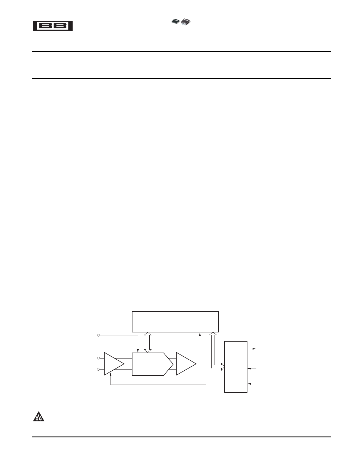
ADS8317
ADS8317
SAR
Serial
Interface
Comparator
ADS8317
S/H Amp
DCLOCK
D
OUT
CS/SHDN
+IN
REF
−
IN
CDAC
查询ADS8317供应商
16-Bit, High-Speed, 2.7V to 5.5V microPower Sampling
ANALOG-TO-DIGITAL CONVERTER
1
FEATURES DESCRIPTION
23
• 16 Bits No Missing Codes (Full-Supply Range,
High or Low Grade)
• Very Low Noise: 5LSB
• Excellent Linearity:
± 0.8LSB typ, ± 1.5LSB max INL
+0.7LSB typ, +1.25LSB max DNL
± 1mV max Offset
± 16LSB typ Gain Error
• microPower:
10mW at 5V, 250kHz
4mW at 2.7V, 200kHz
2mW at 2.7V, 100kHz
0.2mW at 2.7V, 10kHz
• MSOP-8 Package
(SON-8 package available Q1, 2008; package
size same as 3x3 QFN)
• Pin-Compatible with the ADS8321
• Serial ( SPI™/SSI) Interface
PP
ADS8317
SBAS356A – JUNE 2007 – REVISED SEPTEMBER 2007
The ADS8317 is a 16-bit, sampling, analog-to-digital
(A/D) converter specified for a supply voltage range
from 2.7V to 5.5V. It requires very little power, even
when operating at the full data rate. At lower data
rates, the high speed of the device enables it to
spend most of its time in the power-down mode. For
example, the average power dissipation is less than
0.2mW at a 10kHz data rate.
The ADS8317 offers excellent linearity and very low
noise and distortion. It also features a synchronous
serial (SPI/SSI-compatible) interface and a differential
input. The reference voltage can be set to any level
within the range of 0.1V to V
Low power and small size make the ADS8317 ideal
for portable and battery-operated systems. It is also
an excellent fit for remote data-acquisition modules,
simultaneous multichannel systems, and isolated
data acquisition. The ADS8317 is available in
MSOP-8 and SON-8 packages. The SON package
size is the same as a 3x3 QFN package.
/2.
DD
APPLICATIONS
• Battery-Operated Systems
• Remote Data Acquisition
• Isolated Data Acquisition
• Simultaneous Sampling, Multichannel
Systems
• Industrial Controls
• Robotics
• Vibration Analysis
1
Please be aware that an important notice concerning availability, standard warranty, and use in critical applications of
Texas Instruments semiconductor products and disclaimers thereto appears at the end of this data sheet.
2 SPI is a trademark of Motorola, Inc.
3 All other trademarks are the property of their respective owners.
PRODUCTION DATA information is current as of publication date.
Products conform to specifications per the terms of the Texas
Instruments standard warranty. Production processing does not
necessarily include testing of all parameters.
Copyright © 2007, Texas Instruments Incorporated
Page 2
www.ti.com
ADS8317
SBAS356A – JUNE 2007 – REVISED SEPTEMBER 2007
This integrated circuit can be damaged by ESD. Texas Instruments recommends that all integrated circuits be handled with
appropriate precautions. Failure to observe proper handling and installation procedures can cause damage.
ESD damage can range from subtle performance degradation to complete device failure. Precision integrated circuits may be more
susceptible to damage because very small parametric changes could cause the device not to meet its published specifications.
ORDERING INFORMATION
MAXIMUM NO
INTEGRAL MISSING
LINEARITY CODES SPECIFIED TRANSPORT
ERROR ERROR PACKAGE- PACKAGE TEMPERATURE PACKAGE ORDERING MEDIA,
PRODUCT (LSB)
ADS8317I ± 2 16 MSOP-8 DGK – 40 ° C to +85 ° C D17
ADS8317IB ± 1.5 16 MSOP-8 DGK – 40 ° C to +85 ° C D17
ADS8317I
ADS8317IB
(3)
(3)
(2)
(LSB) LEAD DESIGNATOR RANGE MARKING NUMBER QUANTITY
± 2 16 SON-8 DRB – 40 ° C to +85 ° C D17
± 1.5 16 SON-8 DRB – 40 ° C to +85 ° C D17
(1)
ADS8317IDGKT Tape and Reel, 250
ADS8317IDGKR Tape and Reel, 2500
ADS8317IBDGKT Tape and Reel, 250
ADS8317IBDGKR Tape and Reel, 2500
ADS8317IDRBT Tape and Reel, 250
ADS8317IDRBR Tape and Reel, 2500
ADS8317IBDRBT Tape and Reel, 250
ADS8317IBDRBR Tape and Reel, 2500
(1) For the most current package and ordering information, see the Package Option Addendum located at the end of this data sheet, or see
the TI website at www.ti.com.
(2) Maximum Integral Linearity Error specifies a 5V power supply and 2.5V reference voltage.
(3) DRB (SON-8) package available Q1, 2008.
ABSOLUTE MAXIMUM RATINGS
(1)
Over operating free-air temperature range (unless otherwise noted).
ADS8317 UNIT
Supply voltage, V
Analog input voltage
Reference input voltage
Digital input voltage
Input current to any pin except supply – 20 to +20 mA
Power dissipation See Dissipation Ratings Table
Operating virtual junction temperature range, T
Operating free-air temperature range, T
Storage temperature range, T
Lead Temperature 1.6mm (1/16 inch) from case for 10sec +260 ° C
(1) Stresses beyond those listed under Absolute Maximum Ratings may cause permanent damage to the device. These are stress ratings
only, and functional operation of the device at these or any other conditions beyond those indicated under Recommended Operating
Conditions is not implied. Exposure to absolute-maximum rated conditions for extended periods may affect device reliability.
(2) All voltage values are with respect to ground terminal.
to GND – 0.3 to +7 V
DD
(2)
(2)
(2)
J
A
STG
– 0.3 to V
– 0.3 to V
– 0.3 to V
+ 0.3 V
DD
+ 0.3 V
DD
+ 0.3 V
DD
– 40 to +150 ° C
– 40 to +85 ° C
– 65 to +150 ° C
DISSIPATION RATINGS
DERATING
PACKAGE R
θ JC
R
θ JA
DGK +39.1 ° C/W +206.3 ° C/W 4.847mW/ ° C 606mW 388mW 315mW
DRB +5 ° C/W +45.8 ° C/W 3.7mW/ ° C 370mW 204mW 148mW
2 Submit Documentation Feedback Copyright © 2007, Texas Instruments Incorporated
FACTOR ABOVE TA≤ +25 ° C TA= +70 ° C TA= +85 ° C
TA= +25 ° C POWER RATING POWER RATING POWER RATING
Product Folder Link(s): ADS8317
Page 3
www.ti.com
SBAS356A – JUNE 2007 – REVISED SEPTEMBER 2007
RECOMMENDED OPERATING CONDITIONS
MIN TYP MAX UNIT
Supply voltage, GND to V
DD
Reference input voltage 1 VDD/2 V
Analog input voltage +IN to GND – 0.2 V
Operating junction temperature, T
J
Low-voltage levels 2.7 3.6 V
5V logic levels 4.5 5.0 5.5 V
– IN to GND – 0.2 V
+IN – ( – IN) – V
REF
+ 0.2 V
DD
+ 0.2 V
DD
+V
REF
– 40 +125 ° C
ADS8317
V
ELECTRICAL CHARACTERISTICS: V
At – 40 ° C to +85 ° C, V
PARAMETER TEST CONDITIONS MIN TYP MAX MIN TYP MAX UNIT
ANALOG INPUT
Full-scale range FSR +IN – ( – IN) – V
Absolute input range +IN – 0.1 VDD+ 0.1 – 0.1 VDD+ 0.1 V
Input resistance R
Input capacitance During sampling 24 24 pF
Input leakage current ± 50 ± 50 nA
Differential input capacitance +IN to – IN, during sampling 20 20 pF
Full-power bandwidth FSBW fSsinewave, SINAD = 60dB 500 500 kHz
DC ACCURACY
Resolution 16 16 Bits
No missing codes NMC 16 16 16 16 Bits
Integral linearity error INL – 2 ± 1.5 +2 – 1.5 ± 0.8 +1.5 LSB
Differential linearity error DNL – 1 ± 1 +2 – 1 +0.7, – 0.5 +1.25 LSB
Offset error V
Offset error drift TCV
Gain error G
Gain error drift TCG
Bipolar zero error – 2 ± 0.75 +2 – 1 ± 0.5 +1 mV
Bipolar zero error drift ± 3 ± 3 μ V/ ° C
Noise 50 50 μ VRMS
Power-supply rejection PSRR 4.75V ≤ VDD≤ 5.25V 1 1 LSB
SAMPLING DYNAMICS
Conversion time
(16 DCLOCKs)
Acquisition time
(4.5 DCLOCKs)
Throughput rate
(22 DCLOCKs)
Clock frequency 0.024 6.0 0.024 6.0 MHz
= +2.5V, – IN = +2.5V, f
REF
Hold 5 5 G Ω
ON
Sampling 50 100 50 100 Ω
OS
OS
Positive – 32 ± 16 +32 – 32 ± 16 +32 LSB
ERR
Negative – 32 ± 16 +32 – 32 ± 16 +32 LSB
ERR
t
24kHz ≤ f
CONV
tAQf
CLK
CLK
= 6.0MHz 0.75 0.75 μ s
= +5V
DD
= 250kHz, and f
SAMPLE
REF
– 2 ± 0.75 +2 – 1 ± 0.5 +1 mV
≤ 6.0MHz 2.667 666.7 2.667 666.7 μ s
= 24 × f
CLK
ADS8317I ADS8317IB
± 3 ± 3 μ V/ ° C
± 0.1 ± 0.1 ppm/ ° C
, unless otherwise noted.
SAMPLE
V
REF
250 250 kSPS
– V
REF
V
REF
V
Copyright © 2007, Texas Instruments Incorporated Submit Documentation Feedback 3
Product Folder Link(s): ADS8317
Page 4

www.ti.com
ADS8317
SBAS356A – JUNE 2007 – REVISED SEPTEMBER 2007
ELECTRICAL CHARACTERISTICS: V
At – 40 ° C to +85 ° C, V
= +2.5V, – IN = +2.5V, f
REF
= +5V (continued)
DD
SAMPLE
= 250kHz, and f
CLK
= 24 × f
SAMPLE
, unless otherwise noted.
ADS8317I ADS8317IB
PARAMETER TEST CONDITIONS MIN TYP MAX MIN TYP MAX UNIT
AC ACCURACY
5V
sinewave at 2kHz – 102 – 106 dB
Total harmonic distortion THD
Spurious-free dynamic range SFDR
Signal-to-noise ratio SNR
Signal-to-noise + distortion SINAD
Effective number of bits ENOB
PP
5V
sinewave at 10kHz – 100 – 104 dB
PP
5V
sinewave at 2kHz 106 110 dB
PP
5V
sinewave at 10kHz 104 109 dB
PP
5V
sinewave at 2kHz 89.6 90 dB
PP
5V
sinewave at 10kHz 89.6 90 dB
PP
5V
sinewave at 2kHz 89.5 89.9 dB
PP
5V
sinewave at 10kHz 89.4 89.8 dB
PP
5V
sinewave at 2kHz 14.57 14.65 Bits
PP
5V
sinewave at 10kHz 14.56 14.63 Bits
PP
VOLTAGE REFERENCE INPUT
Reference voltage 0.5 VDD/2 0.5 VDD/2 V
Reference input resistance
CS = GND, f
CS = V
DD
= 0Hz 5 5 G Ω
SAMPLE
5 5 G Ω
Reference input capacitance 24 24 pF
fS= 250kHz 35 52 35 52 μ A
fS= 200kHz 25 38 25 38 μ A
Reference input current fS= 100kHz 10 15 10 15 μ A
fS= 10kHz 1 2 1 2 μ A
CS = V
DIGITAL INPUTS
(1)
DD
0.1 0.1 μ A
Logic family CMOS CMOS
High-level input voltage V
Low-level input voltage V
IH
IL
0.7 × V
DD
– 0.3 0.3 × V
VDD+ 0.3 0.7 × V
DD
DD
VDD+ 0.3 V
– 0.3 0.3 × V
DD
Input current IINVI= VDDor GND – 50 +50 – 50 +50 nA
Input capacitance C
DIGITAL OUTPUTS
(1)
I
5 5 pF
Logic family CMOS CMOS
High-level output voltage V
Low-level output voltage V
High-impedance state output
current
Output capacitance C
Load capacitance C
VDD= 4.5V, IOH= – 100A 4.44 4.44 V
OH
VDD= 4.5V, IOL= 100A 0.5 0.5 V
OL
IOZCS = VDD, VI= VDDor GND – 50 +50 – 50 +50 nA
O
L
5 5 pF
30 30 pF
Data format Binary twos complement Binary twos complement
(1) Applies for 5.0V nominal supply: V
(min) = 4.5V and V
DD
(max) = 5.5V.
DD
V
4 Submit Documentation Feedback Copyright © 2007, Texas Instruments Incorporated
Product Folder Link(s): ADS8317
Page 5
www.ti.com
ADS8317
SBAS356A – JUNE 2007 – REVISED SEPTEMBER 2007
ELECTRICAL CHARACTERISTICS: V
At – 40 ° C to +85 ° C, V
= +1.25V, – IN = 1.25V, f
REF
= +2.7V
DD
SAMPLE
= 200kHz, and f
CLK
= 24 × f
SAMPLE
, unless otherwise noted.
ADS8317I ADS8317IB
PARAMETER TEST CONDITIONS MIN TYP MAX MIN TYP MAX UNIT
ANALOG INPUT
Full-scale range FSR +IN – ( – IN) – V
REF
V
REF
– V
REF
V
REF
Absolute input range +IN – 0.1 VDD+ 0.1 – 0.1 VDD+ 0.1 V
Input resistance R
Hold 5 5 G Ω
ON
Sampling 100 150 100 150 Ω
Input capacitance During sampling 24 24 pF
Input leakage current ± 50 ± 50 nA
Differential input capacitance +IN to – IN, during sampling 20 20 pF
Full-power bandwidth FSBW fSsinewave, SINAD = 60dB 1000 1000 kHz
DC ACCURACY
Resolution 16 16 Bits
No missing codes NMC 16 16 16 16 Bits
Integral linearity error INL – 3 ± 2 +3 – 2 ± 1.5 +2 LSB
Differential linearity error DNL – 1 +1.5, – 1 +2.5 – 1 ± 1 +2 LSB
Offset error V
Offset error drift TCV
Gain error G
Gain error drift TCG
OS
OS
Positive – 32 ± 16 +32 – 32 ± 16 +32 LSB
ERR
Negative – 32 ± 16 +32 – 32 ± 16 +32 LSB
ERR
– 2 ± 1 +2 – 1 ± 0.5 +1 mV
± 0.4 ± 0.4 μ V/ ° C
± 0.15 ± 0.15 ppm/ ° C
Bipolar zero error – 2 ± 0.8 +2 – 1 ± 0.4 +1 mV
Bipolar zero error drift ± 0.2 ± 0.2 μ V/ ° C
Noise 50 50 μ VRMS
Power-supply rejection PSRR 2.7V ≤ VDD≤ 3.6V 1 1 LSB
SAMPLING DYNAMICS
Conversion time (16 DCLOCKs) t
Acquisition time (4.5 DCLOCKs) tAQf
24kHz ≤ f
CONV
CLK
≤ 4.8MHz 3.333 666.7 3.333 666.7 μ s
CLK
= 4.8MHz 0.9375 0.9375 μ s
Throughput rate (22 DCLOCKs) 200 200 kSPS
Clock frequency 0.024 4.8 0.024 4.8 MHz
AC ACCURACY
2.5V
sinewave at 2kHz – 104 – 107 dB
Total harmonic distortion THD
Spurious-free dynamic range SFDR
Signal-to-noise ratio SNR
Signal-to-noise + distortion SINAD
Effective number of bits ENOB
PP
2.5V
sinewave at 10kHz – 101 – 106 dB
PP
2.5V
sinewave at 2kHz 106 108 dB
PP
2.5V
sinewave at 10kHz 104 107 dB
PP
2.5V
sinewave at 2kHz 84.8 85 dB
PP
2.5V
sinewave at 10kHz 84.8 85 dB
PP
2.5V
sinewave at 2kHz 84.7 84.9 dB
PP
2.5V
sinewave at 10kHz 84.7 84.8 dB
PP
2.5V
sinewave at 2kHz 13.77 13.8 Bits
PP
2.5V
sinewave at 10kHz 13.77 13.79 Bits
PP
VOLTAGE REFERENCE INPUT
Reference voltage 1 VDD/2 1 VDD/2 V
Reference input resistance
CS = GND, f
CS = V
DD
= 0Hz 5 5 k Ω
SAMPLE
5 5 G Ω
Reference input capacitance 20 20 pF
fS= 200kHz 9 14 9 14 μ A
Reference input current
fS= 100kHz 3 5 3 5 μ A
fS= 10kHz 0.5 1 0.5 1 μ A
CS = V
DD
0.1 0.1 μ A
V
Copyright © 2007, Texas Instruments Incorporated Submit Documentation Feedback 5
Product Folder Link(s): ADS8317
Page 6
www.ti.com
ADS8317
SBAS356A – JUNE 2007 – REVISED SEPTEMBER 2007
ELECTRICAL CHARACTERISTICS: V
At – 40 ° C to +85 ° C, V
= +1.25V, – IN = 1.25V, f
REF
= +2.7V (continued)
DD
SAMPLE
= 200kHz, and f
CLK
= 24 × f
SAMPLE
, unless otherwise noted.
ADS8317I ADS8317IB
PARAMETER TEST CONDITIONS MIN TYP MAX MIN TYP MAX UNIT
DIGITAL INPUTS
(1)
Logic family LVCMOS LVCMOS
High-level input voltage V
Low-level input voltage VILVDD= 2.7V – 0.3 0.8 – 0.3 0.3 × V
VDD= 3.6V 2 VDD+ 0.3 2 VDD+ 0.3 V
IH
DD
Input current IINVI= VDDor GND – 50 +50 – 50 +50 nA
Input capacitance C
DIGITAL OUTPUTS
(1)
I
5 5 pF
Logic family LVCMOS LVCMOS
High-level output voltage V
Low-level output voltage V
High-impedance state output
current
Output capacitance C
Load capacitance C
VDD= 2.7V, IOH= – 100A VDD– 0.2 VDD– 0.2 V
OH
VDD= 2.7V, IOL= 100A 0.2 0.2 V
OL
IOZCS = VDD, VI= VDDor GND – 50 +50 – 50 +50 nA
O
L
5 5 pF
30 30 pF
Data format Binary twos complement Binary twos complement
(1) Applies for 5.0V nominal supply: V
(min) = 2.7V and V
DD
(max) = 3.6V.
DD
ELECTRICAL CHARACTERISTICS: GENERAL
At – 40 ° C to +85 ° C, – IN = GND, and f
PARAMETER TEST CONDITIONS MIN TYP MAX MIN TYP MAX UNIT
ANALOG INPUT
Power supply V
Operating supply current I
Power-down supply current I
Power dissipation 3.8 5.4 3.8 5.4 mW
Power dissipation in power-down
Low-voltage levels 2.7 3.6 2.7 3.6 V
DD
5V logic levels 4.5 5.5 4.5 5.5 V
VDD= 2.7V, fS= 10kHz,
f
DCLOCK
VDD= 2.7V, fS= 100kHz,
f
DCLOCK
VDD= 2.7V, fS= 200kHz,
DD
f
DCLOCK
VDD= 5V, fS= 200kHz,
f
DCLOCK
VDD= 5V, fS= 250kHz,
f
DCLOCK
VDD= 2.7V 0.1 0.1 μ A
DD
VDD= 5V 0.2 0.2 μ A
VDD= 2.7V, fS= 10kHz,
f
DCLOCK
VDD= 2.7V, fS= 100kHz,
f
DCLOCK
VDD= 2.7V, fS= 200kHz,
f
DCLOCK
VDD= 5V, fS= 200kHz,
f
DCLOCK
VDD= 5V, fS= 250kHz,
f
DCLOCK
VDD= 2.7V, CS = V
VDD= 5V, CS = V
= 24 × f
DCLOCK
SAMPLE
, unless otherwise noted.
ADS8317I ADS8317IB
= 4.8MHz
= 4.8MHz
= 4.8MHz
= 6MHz
= 6MHz
= 4.8MHz
= 4.8MHz
0.065 0.085 0.065 0.085 mA
0.7 1.0 0.7 1.0 mA
1.4 2.0 1.4 2.0 mA
1.5 2.5 1.5 2.5 mA
2.0 3.0 2.0 3.0 mA
0.18 0.23 0.18 0.23 mW
1.9 2.7 1.9 2.7 mW
= 4.8MHz
= 6MHz
= 6MHz
DD
DD
7.5 12.5 7.5 12.5 mW
10 15 10 15 mW
0.3 0.3 μ W
0.6 0.6 μ W
V
6 Submit Documentation Feedback Copyright © 2007, Texas Instruments Incorporated
Product Folder Link(s): ADS8317
Page 7
www.ti.com
1
2
3
4
8
7
6
5
V
DD
DCLOCK
D
OUT
CS/SHDN
REF
+IN
-IN
GND
ADS8317
REF
+IN
-IN
GND
V
DD
DCLOCK
D
OUT
CS/SHDN
1
2
3
4
8
7
6
5
ADS8317
(ThermalPad)
R
50W
ON
C
(SAMPLE)
24pF
V
DD
I/O
GND
V
DD
ANALOGIN
GND
DiodeTurn-OnVoltage:0.35V
EquivalentAnalogInputCircuit
V
DD
REF
GND
EquivalentReferenceInputCircuit
EquivalentDigitalInput/OutputCircuit
24pF
R
50W
ON
ADS8317
SBAS356A – JUNE 2007 – REVISED SEPTEMBER 2007
PIN CONFIGURATION
DGK PACKAGE
MSOP-8
(TOP VIEW)
DRB PACKAGE
(1)(2)
SON-8
(TOP VIEW)
(1) DRB package (SON-8) available Q1, 2008.
(2) The DRB package thermal pad must be soldered to the printed circuit board for proper thermal and mechanical
performance.
TERMINAL FUNCTIONS
TERMINAL
NAME NO. I/O DESCRIPTION
REF 1 Analog input Reference input
+IN 2 Analog input Noninverting analog input
– IN 3 Analog input Inverting analog input
GND 4 Power-supply connection Ground
CS/SHDN 5 Digital input Chip select when low; Shutdown mode when high.
D
OUT
DCLOCK 7 Digital input Data clock synchronizes the serial data transfer and determines conversion speed.
V
DD
6 Digital output Serial output data word
8 Power-supply connection Power supply
Equivalent Input Circuits (V
Copyright © 2007, Texas Instruments Incorporated Submit Documentation Feedback 7
= 5.0V)
DD
Product Folder Link(s): ADS8317
Page 8
www.ti.com
D
OUT
1.4V
TestPoint
3kW
100pF
C
LOAD
LoadCircuitfort ,t ,andt
dDO r f
VoltageWaveformsforD RiseandFallTimes,t ,t
OUT r f
VoltageWaveformsforD DelayTimes,t
OUT dDO
VoltageWaveformsfort
dis
VoltageWaveformsfort
en
LoadCircuitfort andt
dis en
t
r
D
OUT
90%
10%
t
f
D
OUT
TestPoint
t Waveform2,t
dis en
V
DD
t Waveform1
dis
100pF
C
LOAD
3kW
t
dis
CS/SHDN
D
OUT
Waveform1
(3)
D
OUT
Waveform2
(4)
90%
10%
90%
41
B15
5
t
en
CS/SHDN
DCLOCK
D
OUT
t
dDO
D
OUT
DCLOCK
t
hDO
(3)Waveform1isforanoutputwithinternalconditionssuchthat
theoutputishighunlessdisabledbytheoutputcontrol.
(4)Waveform2isforanoutputwithinternalconditionssuchthat
theoutputislowunlessdisabledbytheoutputcontrol.
CS/SHDN
D
OUT
DCLOCK
t
CYC
PowerDown
ConversionSample
Usepositiveclockedgefordatatransfer
t
SUCS
t
CONV
t
SMPL
NOTE:(1)Aminimumof22clockcyclesarerequiredfor16-bitconversion;24clockcyclesareshown.
If remainslowattheendofconversion,anewdatastreamisshiftedoutwithLSB-firstdatafollowedbyzeroesindefinitely.CS
B15
(MSB)
B14 B13 B12 B11 B10 B9 B8
B0
(1)
(LSB)
B7 B1B6 B2B5 B3B4
Hi-Z
0
Hi-Z
t
CSD
NOTES:
CS/SHDN
D
OUT
DCLOCK
t
CONV
t
SUCS
t
CSD
t
CYC
PowerDown
t
SMPL
NOTE:(2)Aftercompletingthedatatransfer,iffurtherclocksareappliedwith low,theA/Dconverterwilloutputzeroesindefinitely.CS
B15
(MSB)
B14 B13 B12 B11 B6 B5 B4 B4B3 B3B2 B2B1 B1B0
Null
Bit
Hi-Z Hi-Z
B5 B0 B11 B12 B13 B14
B15
(2)
(LSB) (MSB)
ADS8317
SBAS356A – JUNE 2007 – REVISED SEPTEMBER 2007
TIMING INFORMATION
8 Submit Documentation Feedback Copyright © 2007, Texas Instruments Incorporated
Figure 1. Timing Diagrams
Product Folder Link(s): ADS8317
Page 9
www.ti.com
SBAS356A – JUNE 2007 – REVISED SEPTEMBER 2007
TIMING INFORMATION (continued)
Timing Characteristics
SYMBOL DESCRIPTION MIN TYP MAX UNIT
t
SMPL
t
CONV
t
CYC
t
CSD
t
SUCS
t
HDO
t
DIS
t
EN
t
F
t
R
Analog input sample time 4.5 5.0 DCLOCKs
Conversion time 16 DCLOCKs
Complete cycle time 22 DCLOCKs
CS falling to DCLOCK low 0 ns
CS falling to DCLOCK rising 20 ns
DCLOCK falling to current D
CS rising to D
DCLOCK falling to D
D
fall time 5 25 ns
OUT
D
rise time 7 25 ns
OUT
3-state 70 100 ns
OUT
OUT
not valid 5 15 ns
OUT
enabled 20 50 ns
ADS8317
Copyright © 2007, Texas Instruments Incorporated Submit Documentation Feedback 9
Product Folder Link(s): ADS8317
Page 10

www.ti.com
3
2
1
0
-1
-2
-3
ILE(LSB)
8000h C000h 0000h 4000h 7FFFh
OutputCode
3
2
1
0
-1
-2
-3
DLE(LSB)
8000h C000h 0000h 4000h 7FFFh
OutputCode
1.750
1.745
1.740
1.735
1.730
1.725
1.720
1.715
1.710
SupplyCurrent(mA)
-50 -25 0 25 50
75 100
Temperature(°C)
3.0
2.5
2.0
1.5
1.0
0.5
0
-0.5
-1.0
-1.5
-2.0
Deltafrom+25
C(LSB)°
-50 -25 0 25 50
75 100
Temperature( C)°
3.0
2.5
2.0
1.5
1.0
0.5
0
-0.5
-1.0
-1.5
-2.0
Deltafrom+25
C(LSB)°
-50 -25 0 25 50
75 100
Temperature( C)°
0.50
0.25
0
-0.25
-0.50
-0.75
Deltafrom+25 C(LSB)°
-50 -25 0 25 50
75 100
Temperature( C)°
ADS8317
SBAS356A – JUNE 2007 – REVISED SEPTEMBER 2007
At TA= 25 ° C, V
TYPICAL CHARACTERISTICS: V
REF
= 2.5V, f
SAMPLE
= 250kHz, f
CLK
= 24 × f
DD
SAMPLE
= +5V
, unless otherwise noted.
INTEGRAL LINEARITY ERROR DIFFERENTIAL LINEARITY ERROR
vs CODE vs CODE
Figure 2. Figure 3.
SUPPLY CURRENT CHANGE IN OFFSET
vs TEMPERATURE vs TEMPERATURE
Figure 4. Figure 5.
CHANGE IN BIPOLAR ZERO ERROR CHANGE IN GAIN
vs TEMPERATURE vs TEMPERATURE
10 Submit Documentation Feedback Copyright © 2007, Texas Instruments Incorporated
Figure 6. Figure 7.
Product Folder Link(s): ADS8317
Page 11

www.ti.com
38
37
36
35
34
33
32
31
30
29
28
27
26
25
24
P
ower
-DownCurrent(nA)
-50 -25 0 25 50
75
100
Temperature( C)°
10
1
0.1
0.01
0.001
SupplyCurrent(mA)
1 10 100
250
SamplingRate(kHz)
100
10
1
0.1
0.01
SupplyCurrent(mA)
1 10 100
250
SamplingRate(kHz)
0
-20
-40
-60
-80
-100
-120
-140
-160
Amplitude(dB)
0 5025 75 100 125
Frequency(kHz)
95
90
85
80
75
SNRandSINAD(dB)
1 10 100
200
Frequency(kHz)
SINAD
SNR
0
-20
-40
-60
-80
-100
-120
-140
-160
Amplitude(dB)
0 5025 75 100 125
Frequency(kHz)
ADS8317
SBAS356A – JUNE 2007 – REVISED SEPTEMBER 2007
At TA= 25 ° C, V
REF
= 2.5V, f
TYPICAL CHARACTERISTICS: V
SAMPLE
= 250kHz, f
CLK
= 24 × f
SAMPLE
, unless otherwise noted.
DD
POWER-DOWN CURRENT SUPPLY CURRENT
vs TEMPERATURE vs SAMPLING RATE
Figure 8. Figure 9.
REFERENCE CURRENT FREQUENCY SPECTRUM
vs SAMPLING RATE (8192 point FFT, fIN= 1.9836kHz, – 0.2dB)
= +5V (continued)
FREQUENCY SPECTRUM AND SIGNAL-TO-NOISE + DISTORTION
(8192 Point FFT, fIN= 9.9792kHz, – 0.2dB) vs INPUT FREQUENCY
Copyright © 2007, Texas Instruments Incorporated Submit Documentation Feedback 11
Figure 10. Figure 11.
SIGNAL-TO-NOISE RATIO
Figure 12. Figure 13.
Product Folder Link(s): ADS8317
Page 12

www.ti.com
120
115
110
105
100
95
90
85
80
75
70
65
-120
-115
-110
-105
-100
-95
-90
-85
-80
-75
-70
-65
SFDR(dB)
1 10 100
200
Frequency(kHz)
THD
(1)
SFDR
NOTE:(1)Firstnineharmonicsoftheinputfrequency.
THD(dB)
15.0
14.5
14.0
13.5
13.0
12.5
12.0
ENOB(Bits)
1 10 100
200
Frequency(kHz)
0.7
0.6
0.5
0.4
0.3
0.2
0.1
0
-0.1
-0.2
-0.3
-0.4
-0.5
Deltafrom+25
C(LSB)°
-50 -25 0 25 50
75 100
Temperature( C)°
fIN=1.98364kHz, -0.2dB
100
90
80
70
60
50
40
30
20
10
SINAD(dB)
f =1.98364kHz
IN
-80 -70 -60 -50 -40 -30 -20 -10
0
InputLevel(dB)
FFFF 0000
0002
FFFE
34 42
1673
4835
1608
0001
Code(Hex)
100
10
1
Peak-to-PeakNoise(LSB)
0.1
2.51 2
ReferenceVoltage(V)
V =5V
DD
ADS8317
SBAS356A – JUNE 2007 – REVISED SEPTEMBER 2007
At TA= 25 ° C, V
REF
= 2.5V, f
TYPICAL CHARACTERISTICS: V
SAMPLE
= 250kHz, f
CLK
= 24 × f
SAMPLE
, unless otherwise noted.
= +5V (continued)
DD
SPURIOUS-FREE DYNAMIC RANGE
AND TOTAL HARMONIC DISTORTION EFFECTIVE NUMBER OF BITS
vs INPUT FREQUENCY vs INPUT FREQUENCY
Figure 14. Figure 15.
CHANGE IN SIGNAL-TO-NOISE + DISTORTION CHANGE IN SIGNAL-TO-NOISE + DISTORTION
vs TEMPERATURE vs INPUT LEVEL
PEAK-TO-PEAK NOISE FOR A DC INPUT OUTPUT CODE HISTOGRAM FOR A DC INPUT
vs REFERENCE VOLTAGE (8192 Conversions)
12 Submit Documentation Feedback Copyright © 2007, Texas Instruments Incorporated
Figure 16. Figure 17.
Product Folder Link(s): ADS8317
Figure 18. Figure 19.
Page 13

www.ti.com
3
2
1
0
-1
-2
-3
ILE(LSB)
8000h C000h 0000h 4000h 7FFFh
OutputCode
3
2
1
0
-1
-2
-3
DLE(LSB)
8000h C000h 0000h 4000h 7FFFh
OutputCode
1.310
1.305
1.300
1.295
1.290
1.285
1.280
1.275
1.270
1.265
1.260
SupplyCurrent(mA)
-50 -25 0 25 50
75 100
Temperature( C)°
1.00
0.75
0.50
0.25
0
-0.25
-0.50
-0.75
-1.00
Deltafrom+25 C(LSB)°
-50 -25 0 25 50
75 100
Temperature( C)°
0.50
0.25
0
-0.25
-0.50
Deltafrom+25 C(LSB)°
-50 -25 0 25 50
75 100
Temperature( C)°
0.50
0.25
0
-0.25
-0.50
-0.75
-1.00
Deltafrom+25 C(LSB)°
-50 -25 0 25 50
75 100
Temperature( C)°
ADS8317
SBAS356A – JUNE 2007 – REVISED SEPTEMBER 2007
At TA= 25 ° C, V
TYPICAL CHARACTERISTICS: V
REF
= 1.25V, f
SAMPLE
= 200kHz, f
CLK
= 24 × f
= +2.7V
DD
SAMPLE
, unless otherwise noted.
INTEGRAL LINEARITY ERROR DIFFERENTIAL LINEARITY ERROR
vs CODE vs CODE
Figure 20. Figure 21.
SUPPLY CURRENT CHANGE IN OFFSET
vs TEMPERATURE vs TEMPERATURE
Figure 22. Figure 23.
CHANGE IN BIPOLAR ZERO ERROR CHANGE IN GAIN
vs TEMPERATURE vs TEMPERATURE
Copyright © 2007, Texas Instruments Incorporated Submit Documentation Feedback 13
Figure 24. Figure 25.
Product Folder Link(s): ADS8317
Page 14

www.ti.com
25
24
23
22
21
20
19
18
17
16
Power
-DownCurrent(nA)
-50 -25 0 25 50
75 100
Temperature( C)°
10
1
0.1
0.01
0.001
0.0001
SupplyCurrent(mA)
1
20010 100
SamplingRate(kHz)
100
10
1
0.1
0.01
ReferenceCurrent( A)
m
1
20010 100
SamplingRate(kHz)
0
-20
-40
-60
-80
-100
-120
-140
-160
Amplitude(dB)
0 402010 60 805030 70 90 100
Frequency(kHz)
86
85
84
83
82
81
80
79
78
SNRandSINAD(dB)
1 10 100
200
Frequency(kHz)
SINAD
SNR
0
-20
-40
-60
-80
-100
-120
-140
-160
Amplitude(dB)
0 402010 60 805030 70 90 100
Frequency(kHz)
ADS8317
SBAS356A – JUNE 2007 – REVISED SEPTEMBER 2007
At TA= 25 ° C, V
REF
= 1.25V, f
TYPICAL CHARACTERISTICS: V
SAMPLE
= 200kHz, f
CLK
= 24 × f
SAMPLE
, unless otherwise noted.
= +2.7V (continued)
DD
POWER-DOWN CURRENT SUPPLY CURRENT
vs TEMPERATURE vs SAMPLING RATE
Figure 26. Figure 27.
REFERENCE CURRENT FREQUENCY SPECTRUM
vs SAMPLING RATE (8192 Point FFT, fIN = 1.9775kHz, – 0.2dB)
FREQUENCY SPECTRUM AND SIGNAL-TO-NOISE + DISTORTION
(8192 Point FFT, fIN= 9.9854kHz, – 0.2dB) vs INPUT FREQUENCY
14 Submit Documentation Feedback Copyright © 2007, Texas Instruments Incorporated
Figure 28. Figure 29.
SIGNAL-TO-NOISE RATIO
Figure 30. Figure 31.
Product Folder Link(s): ADS8317
Page 15

www.ti.com
110
105
100
95
90
85
80
-110
-105
-100
-95
-90
-85
-80
SFDR(dB)
THD(dB)
1 10 100
200
Frequency(kHz)
THD
(1)
SFDR
NOTE:(1)Firstnineharmonicsoftheinputfrequency.
15.0
14.5
14.0
13.5
13.0
12.5
12.0
ENOB(Bits)
1 10 100
200
Frequency(kHz)
0.6
0.5
0.4
0.3
0.2
0.1
0
-0.1
-0.2
-0.3
-0.4
-0.5
-0.6
Deltafrom+25
C(LSB)°
-50 -25 0 25 50
75 100
Temperature( C)°
f =1.97754kHz, 0.2dB-
IN
100
90
80
70
60
50
40
30
20
10
0
SINAD(dB)
-80 -70 -60 -50 -40 -30 -20 -10
0
InputLevel(dB)
f =1.97754kHz
IN
FFFE FFFFFFFD 0000
0002 0003 0004
FFFC
3920
1596
1504
497
50
1
581
41
2
0001
Code(Hex)
ADS8317
SBAS356A – JUNE 2007 – REVISED SEPTEMBER 2007
At TA= 25 ° C, V
REF
= 1.25V, f
TYPICAL CHARACTERISTICS: V
SAMPLE
= 200kHz, f
CLK
= 24 × f
SAMPLE
, unless otherwise noted.
= +2.7V (continued)
DD
SPURIOUS-FREE DYNAMIC RANGE
AND TOTAL HARMONIC DISTORTION EFFECTIVE NUMBER OF BITS
vs INPUT FREQUENCY vs INPUT FREQUENCY
Figure 32. Figure 33.
CHANGE IN SIGNAL-TO-NOISE + DISTORTION SIGNAL-TO-NOISE + DISTORTION
vs TEMPERATURE vs INPUT LEVEL
Copyright © 2007, Texas Instruments Incorporated Submit Documentation Feedback 15
Figure 34. Figure 35.
OUTPUT CODE HISTOGRAM FOR A DC INPUT
(8192 Conversions)
Figure 36.
Product Folder Link(s): ADS8317
Page 16

www.ti.com
ADS8317
ADS8317
Single-EndedInput
Common
Voltage
2 V´
REF
Peak-to-Peak
DifferentialInput
Common
Voltage
V
REF
Peak-to-Peak
V
REF
Peak-to-Peak
ADS8317
SBAS356A – JUNE 2007 – REVISED SEPTEMBER 2007
THEORY OF OPERATION
The ADS8317 is a classic Successive Approximation
Register (SAR) analog-to-digital (A/D) converter. The
architecture is based on capacitive redistribution that
inherently includes a sample-and-hold function. The
converter is fabricated on a 0.6 μ CMOS process. The
architecture and fabrication process allow the
ADS8317 to acquire and convert an analog signal at
up to 250,000 conversions per second while
consuming less than 10mW from V
.
DD
Differential linearity for the ADS8317 is
factory-adjusted via a package-level trim procedure.
The state of the trim elements is stored in non-volatile
memory and is continuously updated after each
acquisition cycle, just prior to the start of the
successive approximation operation. This process
ensures that one complete conversion cycle always
returns the part to its factory-adjusted state in the
event of a power interruption.
The ADS8317 requires an external reference, an
external clock, and a single power source (V
). The
DD
external reference can be any voltage between 0.1V
and V
/2. The value of the reference voltage directly
DD
sets the range of the analog input. The reference
input current depends on the conversion rate of the
ADS8317.
The external clock can vary between 24kHz (1kHz
throughput) and 6.0MHz (250kHz throughput). The
duty cycle of the clock is not significant, as long as
the minimum high and low times are at least 200ns
(V
= 4.75V or greater). The minimum clock
DD
frequency is set by the leakage on the internal
capacitors to the ADS8317.
The analog input is provided to two input pins: +IN
and – IN. When a conversion is initiated, the
differential input on these pins is sampled on the
internal capacitor array. While a conversion is in ADS8317 — Single-Ended or Differential
progress, both inputs are disconnected from any
internal function.
The digital result of the conversion is clocked out by
the DCLOCK input and is provided serially (most
significant bit first) on the D
pin.
OUT
The digital data that are provided on the D
for the conversion currently in progress — there is no
pipeline delay. It is possible to continue to clock the
ADS8317 after the conversion is complete and to
obtain the serial data least significant bit first. See the
Digital Timing section for more information.
ANALOG INPUT
The analog input is bipolar and fully differential. There
are two general methods of driving the analog input
of the ADS8317: single-ended or differential, as
shown in Figure 37 . When the input is single-ended,
the – IN input is held at a fixed voltage. The +IN input
swings around the same voltage and the
peak-to-peak amplitude is 2 × V
V
determines the range over which the common
REF
voltage may vary, as shown in Figure 39 and
Figure 38 .
Figure 37. Methods of Driving the
. The value of
REF
pin are
OUT
16 Submit Documentation Feedback Copyright © 2007, Texas Instruments Incorporated
Product Folder Link(s): ADS8317
Page 17

www.ti.com
5
4
3
2
1
0
-1
CommonVoltageRange(V)
0 0.5 1.0 1.5
2.0 2.5
V (V)
REF
Single-EndedInput
V =5V
DD
3.8
2.8
2.2
-0.3
0
5
4
3
2
1
0
-1
CommonVoltageRange(V)
0 0.5 1.0 1.5
2.0 2.5
V (V)
REF
DifferentialInput
V =5V
DD
3.8
2.75
0.95
-0.3
3.0
2.5
2.0
1.5
1.0
0.5
0
-0.5
-1.0
CommonV
oltageRange(V)
0 0.25 0.50 0.75
1.00 1.25
V (V)
REF
Single-EndedInput
1.5 1.5
0.95
-0.3
V =2.7V
DD
3.0
2.5
2.0
1.5
1.0
0.5
0
-0.5
-1.0
CommonV
oltageRange(V)
0 0.25 0.50 0.75
1.00 1.25
V (V)
REF
DifferentialInput
V =2.7V
DD
1.5 1.5
0.5
-0.3
0
SBAS356A – JUNE 2007 – REVISED SEPTEMBER 2007
Figure 38. Single-Ended 5V Input, Figure 40. Differential 2.7V Input,
Common Voltage Range vs V
REF
Common Voltage Range vs V
ADS8317
REF
Figure 39. Single-Ended 2.7V Input, Figure 41. Differential 2.7V Input,
Common Voltage Range vs V
When the input is differential, the amplitude of the In each case, care should be taken to ensure that the
input is the difference between the +IN and – IN input, output impedance of the sources driving the +IN and
or +IN – ( – IN). A voltage or signal is common to both – IN inputs are matched. If this matching is not
of these inputs. The peak-to-peak amplitude of each observed, the two inputs could have different settling
input is V
about this common voltage. However, times. This difference may result in offset error, gain
REF
since the inputs are 180 ° out-of-phase, the error, and linearity error that change with both
peak-to-peak amplitude of the difference voltage is 2 temperature and input voltage. If the impedance
× V
. The value of V
REF
of the voltage that may be common to both inputs, as giving the ADS8317 additional acquisition time.
shown in Figure 41 and Figure 40 .
Copyright © 2007, Texas Instruments Incorporated Submit Documentation Feedback 17
REF
also determines the range cannot be matched, the errors can be lessened by
REF
Common Voltage Range vs V
Product Folder Link(s): ADS8317
REF
Page 18

www.ti.com
10W
50W
OPA365
24pF
1000pF
1nF
10W
50W
OPA365
24pF
1000pF
+IN
-IN
ADS8326
10W
50W
OPA365
24pF
1000pF
50W
24pF
+IN
-IN
ADS8326
Single-Ended
Differential
V
CM
+
ADS8317
SBAS356A – JUNE 2007 – REVISED SEPTEMBER 2007
The input current on the analog inputs depends on a
number of factors: sample rate, input voltage, and
source impedance. Essentially, the current into the
ADS8317 charges the internal capacitor array during
the sample period. After this capacitance has been
fully charged, there is no further input current. The
source of the analog input voltage must be able to
charge the input capacitance (24pF) to 16-bit settling
level within 4.5 clock cycles. When the converter
goes into the hold mode, or while it is in the
power-down mode, the input impedance is greater
than 1G Ω .
Care must be taken regarding the absolute analog
input voltage. The +IN input should always remain
within the range of GND – 300mV to V
+ 300mW.
DD
The – IN input should always remain within the range
of GND – 300mV to 4V. Outside of these ranges, the
converter linearity may not meet specifications. To
obtain maximum performance from the ADS8317, an
input circuit such as that shown in Figure 42 is
recommended.
REFERENCE INPUT
The external reference sets the analog input range.
The ADS8317 operates with a reference in the range
of 0.1V to V
implications to this specification.
As the reference voltage is reduced, the analog
voltage weight of each digital output code is reduced.
This reduction is often referred to as the least
significant bit (LSB) size and is equal to the reference
voltage divided by 65,536. This relationship means
that any offset or gain error inherent in the A/D
converter appears to increase (in terms of LSB size)
as the reference voltage is reduced. For a reference
voltage of 2.5V, the value of the LSB is 76.3V, and
for a reference voltage of 1.25V, the LSB is 38.15 μ V.
The noise inherent in the converter also appears to
increase with a lower LSB size. With a 2.5V
reference, the internal noise of the converter typically
contributes only 5LSB peak-to-peak of potential error
to the output code. When the external reference is
1.25V, the potential error contribution from the
internal noise is almost two times larger (9LSB). The
errors arising from the internal noise are Gaussian in
nature and can be reduced by averaging consecutive
conversion results.
For more information regarding noise, consult
Figure 18 , Peak-to-Peak Noise for a DC Input vs
Reference Voltage. Note that the Effective Number Of
Bits (ENOB) figure is calculated based on the
converter signal-to-(noise + distortion) ratio with a
2kHz, 0dB input signal. SINAD is related to ENOB as
follows:
SINAD = 6.02 × ENOB + 1.76
With lower reference voltages, extra care should be
taken to provide a clean layout including adequate
bypassing, a clean power supply, a low-noise
reference, and a low-noise input signal. Due to the
lower LSB size, the converter is also more sensitive
to external sources of error, such as nearby digital
signals and electromagnetic interference.
/2. There are several important
DD
Figure 42. Single-Ended and Differential Methods
of Interfacing the ADS8317
18 Submit Documentation Feedback Copyright © 2007, Texas Instruments Incorporated
Product Folder Link(s): ADS8317
Page 19

www.ti.com
OPA350
24pF
47 Fm
ADS8317
V
REF
50W
ADS8317
SBAS356A – JUNE 2007 – REVISED SEPTEMBER 2007
The equivalent input circuit for the reference voltage
is presented in Figure 43 . At the same time, an
equivalent capacitor of 24pF is switched. To obtain
optimum performance from the ADS8317, special
care must be taken in designing the interface circuit
to the reference input pin. To ensure a stable
reference voltage, a 47 μ F tantalum capacitor with low
ESR should be connected as close as possible to the
input pin. If a high output impedance reference
source is used, an additional operational amplifier
with a current-limiting resistor must be placed in front
of the capacitors.
Noise
The transition noise of the ADS8317 itself is
extremely low, as shown in Figure 19 and Figure 36 ;
it is much lower than competing A/D converters.
These histograms were generated by applying a
low-noise DC input and initiating 8192 conversions.
The digital output of the A/D converter varies in
output code because of the internal noise of the
ADS8317. This variance is true for all 16-bit,
SAR-type A/D converters. Using a histogram to plot
the output codes, the distribution should appear
bell-shaped with the peak of the bell curve
representing the nominal code for the input value.
The ± 1 σ , ± 2 σ , and ± 3 σ distributions represent 68.3%,
95.5%, and 99.7%, respectively, of all codes. The
transition noise can be calculated by dividing the
number of codes measured by 6, which yields the 3 σ
distribution, or 99.7%, of all codes. Statistically, up to
three codes could fall outside the distribution when
executing 1000 conversions. The ADS8317, with five
output codes for the ± 3 σ distribution, yields less than
Figure 43. Input Reference Circuit and Interface ± 0.8LSB of transition noise. Remember that to
achieve this low-noise performance, the peak-to-peak
When the ADS8317 is in power-down mode, the input
resistance of the reference pin has a value of 5G Ω .
Because the input capacitors must be recharged
before the next conversion starts, an operational
amplifier with good dynamic characteristics, such as
the OPA350 , should be used to buffer the reference
input.
noise of the input signal and reference must be less
than 50 μ V.
Averaging
The noise of the A/D converter can be compensated
by averaging the digital codes. By averaging
conversion results, transition noise is reduced by a
factor of 1/ √ n , where n is the number of averages.
For example, averaging four conversion results
reduces the transition noise from ± 0.8LSB to
± 0.4LSB. Averaging should only be used for input
signals with frequencies near DC.
For AC signals, a digital filter can be used to
low-pass filter and decimate the output codes. This
configuration works in a similar manner to averaging;
for every decimation by 2, the signal-to-noise ratio
improves by 3dB.
Product Folder Link(s): ADS8317
Copyright © 2007, Texas Instruments Incorporated Submit Documentation Feedback 19
Page 20

www.ti.com
ADS8317
SBAS356A – JUNE 2007 – REVISED SEPTEMBER 2007
DIGITAL INTERFACE
After the fifth falling DCLOCK edge, D
is enabled
OUT
and outputs a low value for one clock period. For the
Signal Levels
The ADS8317 has a wide range of power-supply
voltage. The A/D converter, as well as the digital
interface circuit, is designed to accept and operate
from 2.7V up to 5.5V. This voltage range
next 16 DCLOCK periods, D
outputs the
OUT
conversion result, most significant bit first. After the
least significant bit (B0) has been output, subsequent
clocks repeat the output data, but in a least significant
bit first format.
accommodates different logic levels. When the After the most significant bit (B15) has been
ADS8317 power-supply voltage is in the range of repeated, D
will 3-state. Subsequent clocks have
OUT
4.5V to 5.5V (5V logic level), the ADS8317 can be no effect on the converter. A new conversion is
connected directly to another 5V, CMOS-integrated initiated only when CS has been taken high and
circuit. When the ADS8317 power-supply voltage is in returned low.
the range of 2.7V to 3.6V (3V logic level), the
ADS8317 can be connected directly to another 3.3V
LVCMOS integrated circuit.
Serial Interface
Data Format
The output data from the ADS8317 are in binary twos
complement format, as shown in Table 1 and
Figure 44 . The table and figure represent the ideal
The ADS8317 communicates with microprocessors output code for the given input voltage and do not
and other digital systems via a synchronous 3-wire include the effects of offset, gain error, or noise.
serial interface, as illustrated in the Timing
Information section and Timing Characteristics . The Table 1. Ideal Input Voltages and Output Codes
DCLOCK signal synchronizes the data transfer, with
each bit being transmitted on the falling edge of
DCLOCK. Most receiving systems capture the
bitstream on the rising edge of DCLOCK. However, if
the minimum hold time for D
is acceptable, the
OUT
system can use the falling edge of DCLOCK to
capture each bit.
A falling CS signal initiates the conversion and data
transfer. The first 4.5 to 5.0 clock periods of the
DESCRIPTION ANALOG VALUE
Full-scale range 2 × V
Least significant 2 × V
bit (LSB) Code Code
+Full scale +V
Midscale 0V 0000 0000 0000 0000 0000
Midscale – 1 LSB 0V – 1 LSB 1111 1111 1111 1111 FFFF
– Full scale – V
REF
/65536 Binary Hex
REF
– 1 LSB 0111 1111 1111 1111 7FFF
REF
REF
DIGITAL OUTPUT
BINARY TWOS COMPLEMENT
1000 0000 0000 0000 8000
conversion cycle are used to sample the input signal.
20 Submit Documentation Feedback Copyright © 2007, Texas Instruments Incorporated
Product Folder Link(s): ADS8317
Page 21

www.ti.com
0111111111111111
0111111111111110
0111111111111101
1000000000000010
1000000000000001
1000000000000000
0000000000000001
0000000000000000
1111111111111111
Binary TwosComplement
DigitalOutputCode
V = 2.5V
-FS
-
-2.49996V
-2.49992V
-2.49985V
-38.15 Vm
+38.15 Vm
0V
BipolarAnalogInputV V( IN)- -oltage=V(+IN)
1LSB=76.29 Vm
V =2.5V
CM
V =2.5V
REF
V =V =2.5V
+FS REF
V 1LSB=2.499992V
+FS
-
2.499985V
0
1
2
32767
32768
32769
65533
65534
65535
Step
16-BIT
-Full-ScaleCode
MidscaleCode
+Full-ScaleCode
TwosComplementOutput
V =
-FS
8000h
V =0000h
MS
V =7FFFh
+FS
BipolarAnalogInput
V = V-
CODE REF
V =0V
CODE
V =V -
CODE REF
1LSB
ADS8317
SBAS356A – JUNE 2007 – REVISED SEPTEMBER 2007
Copyright © 2007, Texas Instruments Incorporated Submit Documentation Feedback 21
Figure 44. Ideal Conversion Characteristics (Conditions: V
Product Folder Link(s): ADS8317
CM
= 2.5V, V
= 2.5V)
REF
Page 22

www.ti.com
ADS8317
SBAS356A – JUNE 2007 – REVISED SEPTEMBER 2007
POWER DISSIPATION
The architecture of the converter, the semiconductor
fabrication process, and a careful design allow the
ADS8317 to convert at up to a 250kHz rate while
requiring very little power. However, for the absolute
lowest power dissipation, there are several things to
keep in mind.
The power dissipation of the ADS8317 scales directly
with conversion rate. Therefore, the first step to
achieving the lowest power dissipation is to find the
lowest conversion rate that satisfies the system
requirements.
In addition, the ADS8317 goes into Power-Down
mode under two conditions: when the conversion is
complete and whenever CS is high (see the Timing
Characteristics section). Ideally, each conversion
should occur as quickly as possible, preferably at a
6.0MHz clock rate. This way, the converter spends
the longest possible time in power-down mode. This
is very important because the converter not only uses
power on each DCLOCK transition (as is typical for
digital CMOS components), but also uses some
current for the analog circuitry, such as the
comparator. The analog section dissipates power
continuously until power-down mode is entered.
Figure 9 and Figure 27 illustrate the current
consumption of the ADS8317 versus sample rate. For
these graphs, the converter is clocked at maximum
speed regardless of the sample rate. CS is held high
during the remaining sample period.
There is an important distinction between the
power-down mode that is entered after a conversion
is complete and the full power-down mode that is
enabled when CS is high. CS low only shuts down
the analog section. The digital section completely
shuts down only when CS is high. Thus, if CS is left
low at the end of a conversion, and the converter is
continually clocked, the power consumption is not as
low as when CS is high.
Short Cycling
Another way to save power is to use the CS signal to
short-cycle the conversion. The ADS8317 places the
latest data bit on the D
line as it is generated;
OUT
therefore, the converter can easily be short-cycled.
This term means that the conversion can be
terminated at any time. For example, if only 14 bits of
the conversion result are needed, then the conversion
can be terminated (by pulling CS high) after the 14th
bit has been clocked out.
This technique can also be used to lower the power
dissipation (or to increase the conversion rate) in
those applications where an analog signal is being
monitored until some condition becomes true. For
example, if the signal is outside a predetermined
range, the full 16-bit conversion result may not be
needed. If so, the conversion can be terminated after
the first n bits, where n might be as low as 3 or 4.
This technique results in lower power dissipation in
both the converter and the rest of the system
because they spend more time in power-down mode.
22 Submit Documentation Feedback Copyright © 2007, Texas Instruments Incorporated
Product Folder Link(s): ADS8317
Page 23

www.ti.com
ADS8317
SBAS356A – JUNE 2007 – REVISED SEPTEMBER 2007
LAYOUT
For optimum performance, care should be taken with
the physical layout of the ADS8317 circuitry. This
caution is particularly true if the reference voltage is
low and/or the conversion rate is high. At a 250kHz
conversion rate, the ADS8317 makes a bit decision
every 167ns. That is, for each subsequent bit
decision, the digital output must be updated with the
results of the last bit decision, the capacitor array
appropriately switched and charged, and the input to
the comparator settled to a 16-bit level, all within one
The reference should be similarly bypassed with a
47 μ F capacitor. Again, a series resistor and large
capacitor can be used to low-pass filter the reference
voltage. If the reference voltage originates from an op
amp, make sure that the op amp can drive the
bypass capacitor without oscillation (the series
resistor can help in this case). Keep in mind that
while the ADS8317 draws very little current from the
reference on average, there are still instantaneous
current demands placed on the external input and
reference circuitry.
clock cycle. Texas Instruments' OPA365 op amp provides
The basic SAR architecture is sensitive to spikes on
the power supply, reference, and ground connections
that occur just prior to latching the comparator output.
optimum performance for buffering the signal inputs;
the OPA350 can be used to effectively buffer the
reference input.
Thus, during any single conversion for an n-bit SAR Also, keep in mind that the ADS8317 offers no
converter, there are n windows in which large inherent rejection of noise or voltage variation in
external transient voltages can easily affect the regards to the reference input. This characteristic is
conversion result. Such spikes might originate from of particular concern when the reference input is tied
switching power supplies, digital logic, and to the power supply. Any noise and ripple from the
high-power devices, to name a few potential sources. supply appears directly in the digital results. While
This particular source of error can be very difficult to high-frequency noise can be filtered out, as described
track down if the glitch is almost synchronous to the in the previous paragraph, voltage variation resulting
converter DCLOCK signal because the phase from the line frequency (50Hz or 60Hz) can be
difference between the glitch and DCLOCK changes difficult to remove.
with time and temperature, causing sporadic
misoperation.
The GND pin on the ADS8317 should be placed on a
clean ground point. In many cases, this point is the
With these considerations in mind, power to the analog ground. Avoid connecting the GND pin too
ADS8317 should be clean and well-bypassed. A close to the grounding point for a microprocessor,
0.1 μ F ceramic bypass capacitor should be placed as microcontroller, or digital signal processor. If needed,
close as possible to the ADS8317 package. In run a ground trace directly from the converter to the
addition, a 1 μ F to 10 μ F capacitor and a 5 Ω or 10 Ω power-supply connection point. The ideal layout
series resistor may be used to low-pass filter a noisy includes an analog ground plane for the converter
supply. and associated analog circuitry.
Copyright © 2007, Texas Instruments Incorporated Submit Documentation Feedback 23
Product Folder Link(s): ADS8317
Page 24

www.ti.com
+IN
ADS8317
1000pF
10W
-IN
0.1mF
5W
CS
D
OUT
DCLOCK
47mF
IN
GND
OUT
0.47mF
REF
V
DD
REF3225
AV
DD
2.7Vto5V
DV
DD
2.7Vto3.6V
V
CM
+(0Vto2.5V)
GND GND
DSP
TMS320C6xx
or
TMS320C5xx
or
TMS320C2xx
0.1mF 10mF
10mF
+
+
OPA350
OPA365
1000pF
10W
V
CM
OPA365
1nF
10W
2.2mF
ADS8317
SBAS356A – JUNE 2007 – REVISED SEPTEMBER 2007
APPLICATION CIRCUITS
Figure 45 shows an example of a basic data
acquisition system. The ADS8317 input range is
connected to 2.5V or 4.096V. The 5 Ω resistor and
1 μ F to 10 μ F capacitor filters the microcontroller noise
on the supply, as well as any high-frequency noise
from the supply itself. The exact values should be
picked such that the filter provides adequate rejection
of noise. Operational amplifiers and voltage reference
are connected to the analog power supply, AV
DD
.
Figure 45. Example of a Basic Data Acquisition System
24 Submit Documentation Feedback Copyright © 2007, Texas Instruments Incorporated
Product Folder Link(s): ADS8317
Page 25

PACKAGE OPTION ADDENDUM
www.ti.com
5-Oct-2007
PACKAGING INFORMATION
Orderable Device Status
(1)
Package
Type
Package
Drawing
Pins Package
Qty
Eco Plan
ADS8317IBDGKR ACTIVE MSOP DGK 8 2500 Green (RoHS &
no Sb/Br)
ADS8317IBDGKRG4 ACTIVE MSOP DGK 8 2500 Green (RoHS &
no Sb/Br)
ADS8317IBDGKT ACTIVE MSOP DGK 8 250 Green (RoHS &
no Sb/Br)
ADS8317IBDGKTG4 ACTIVE MSOP DGK 8 250 Green (RoHS&
no Sb/Br)
ADS8317IDGKR ACTIVE MSOP DGK 8 2500 Green (RoHS &
no Sb/Br)
ADS8317IDGKRG4 ACTIVE MSOP DGK 8 2500 Green (RoHS &
no Sb/Br)
ADS8317IDGKT ACTIVE MSOP DGK 8 250 Green (RoHS &
no Sb/Br)
ADS8317IDGKTG4 ACTIVE MSOP DGK 8 250 Green (RoHS &
no Sb/Br)
(1)
The marketing status values are defined as follows:
ACTIVE: Product device recommended for new designs.
LIFEBUY: TI has announced that the device will be discontinued, and a lifetime-buy period is in effect.
NRND: Not recommended for new designs. Device is in production to support existing customers, but TI does not recommend using this part in
a new design.
PREVIEW: Device has been announced but is not in production. Samples may or may not be available.
OBSOLETE: TI has discontinued the production of the device.
(2)
Lead/Ball Finish MSL Peak Temp
CU NIPDAU Level-2-260C-1 YEAR
CU NIPDAU Level-2-260C-1 YEAR
CU NIPDAU Level-2-260C-1 YEAR
CU NIPDAU Level-2-260C-1 YEAR
CU NIPDAU Level-2-260C-1 YEAR
CU NIPDAU Level-2-260C-1 YEAR
CU NIPDAU Level-2-260C-1 YEAR
CU NIPDAU Level-2-260C-1 YEAR
(3)
(2)
Eco Plan - The planned eco-friendly classification: Pb-Free (RoHS), Pb-Free (RoHS Exempt), or Green (RoHS & no Sb/Br) - please check
http://www.ti.com/productcontent for the latest availability information and additional product content details.
TBD: The Pb-Free/Green conversion plan has not been defined.
Pb-Free (RoHS): TI's terms "Lead-Free" or "Pb-Free" mean semiconductor products that are compatible with the current RoHS requirements
for all 6 substances, including the requirement that lead not exceed 0.1% by weight in homogeneous materials. Where designed to be soldered
at high temperatures, TI Pb-Free products are suitable for use in specified lead-free processes.
Pb-Free (RoHS Exempt): This component has a RoHS exemption for either 1) lead-based flip-chip solder bumps used between the die and
package, or 2) lead-based die adhesive used between the die and leadframe. The component is otherwise considered Pb-Free (RoHS
compatible) as defined above.
Green (RoHS & no Sb/Br): TI defines "Green" to mean Pb-Free (RoHS compatible), and free of Bromine (Br) and Antimony (Sb) based flame
retardants (Br or Sb do not exceed 0.1% by weight in homogeneous material)
(3)
MSL, Peak Temp. -- The Moisture Sensitivity Level rating according to the JEDEC industry standard classifications, and peak solder
temperature.
Important Information and Disclaimer:The information provided on this page represents TI's knowledge and belief as of the date that it is
provided. TI bases its knowledge and belief on information provided by third parties, and makes no representation or warranty as to the
accuracy of such information. Efforts are underway to better integrate information from third parties. TI has taken and continues to take
reasonable steps to provide representative and accurate information but may not have conducted destructive testing or chemical analysis on
incoming materials and chemicals. TI and TI suppliers consider certain information to be proprietary, and thus CAS numbers and other limited
information may not be available for release.
In no event shall TI's liability arising out of such information exceed the total purchase price of the TI part(s) at issue in this document sold by TI
to Customer on an annual basis.
Addendum-Page 1
Page 26

PACKAGE MATERIALS INFORMATION
www.ti.com
TAPE AND REEL BOX INFORMATION
4-Oct-2007
Device Package Pins Site Reel
Diameter
(mm)
ADS8317IBDGKR DGK 8 SITE 60 330 12 5.3 3.4 1.4 8 12 Q1
ADS8317IBDGKT DGK 8 SITE 60 330 12 5.3 3.4 1.4 8 12 Q1
ADS8317IDGKR DGK 8 SITE 60 330 12 5.3 3.4 1.4 8 12 Q1
ADS8317IDGKT DGK 8 SITE 60 330 12 5.3 3.4 1.4 8 12 Q1
Reel
Width
(mm)
A0 (mm) B0 (mm) K0 (mm) P1
(mm)W(mm)
Pin1
Quadrant
Pack Materials-Page 1
Page 27

PACKAGE MATERIALS INFORMATION
www.ti.com
4-Oct-2007
Device Package Pins Site Length (mm) Width (mm) Height (mm)
ADS8317IBDGKR DGK 8 SITE 60 346.0 346.0 29.0
ADS8317IBDGKT DGK 8 SITE 60 346.0 346.0 29.0
ADS8317IDGKR DGK 8 SITE 60 346.0 346.0 29.0
ADS8317IDGKT DGK 8 SITE60 346.0 346.0 29.0
Pack Materials-Page 2
Page 28

Page 29

IMPORTANT NOTICE
Texas Instruments Incorporated and its subsidiaries (TI) reserve the right to make corrections, modifications, enhancements,
improvements, and other changes to its products and services at any time and to discontinue any product or service without notice.
Customers should obtain the latest relevant information before placing orders and should verify that such information is current and
complete. All products are sold subject to TI’s terms and conditions of sale supplied at the time of order acknowledgment.
TI warrants performance of its hardware products to the specifications applicable at the time of sale in accordance with TI’s
standard warranty. Testing and other quality control techniques are used to the extent TI deems necessary to support this
warranty. Except where mandated by government requirements, testing of all parameters of each product is not necessarily
performed.
TI assumes no liability for applications assistance or customer product design. Customers are responsible for their products and
applications using TI components. To minimize the risks associated with customer products and applications, customers should
provide adequate design and operating safeguards.
TI does not warrant or represent that any license, either express or implied, is granted under any TI patent right, copyright, mask
work right, or other TI intellectual property right relating to any combination, machine, or process in which TI products or services
are used. Information published by TI regarding third-party products or services does not constitute a license from TI to use such
products or services or a warranty or endorsement thereof. Use of such information may require a license from a third party under
the patents or other intellectual property of the third party, or a license from TI under the patents or other intellectual property of TI.
Reproduction of TI information in TI data books or data sheets is permissible only if reproduction is without alteration and is
accompanied by all associated warranties, conditions, limitations, and notices. Reproduction of this information with alteration is an
unfair and deceptive business practice. TI is not responsible or liable for such altered documentation. Information of third parties
may be subject to additional restrictions.
Resale of TI products or services with statements different from or beyond the parameters stated by TI for that product or service
voids all express and any implied warranties for the associated TI product or service and is an unfair and deceptive business
practice. TI is not responsible or liable for any such statements.
TI products are not authorized for use in safety-critical applications (such as life support) where a failure of the TI product would
reasonably be expected to cause severe personal injury or death, unless officers of the parties have executed an agreement
specifically governing such use. Buyers represent that they have all necessary expertise in the safety and regulatory ramifications
of their applications, and acknowledge and agree that they are solely responsible for all legal, regulatory and safety-related
requirements concerning their products and any use of TI products in such safety-critical applications, notwithstanding any
applications-related information or support that may be provided by TI. Further, Buyers must fully indemnify TI and its
representatives against any damages arising out of the use of TI products in such safety-critical applications.
TI products are neither designed nor intended for use in military/aerospace applications or environments unless the TI products are
specifically designated by TI as military-grade or "enhanced plastic." Only products designated by TI as military-grade meet military
specifications. Buyers acknowledge and agree that any such use of TI products which TI has not designated as military-grade is
solely at the Buyer's risk, and that they are solely responsible for compliance with all legal and regulatory requirements in
connection with such use.
TI products are neither designed nor intended for use in automotive applications or environments unless the specific TI products
are designated by TI as compliant with ISO/TS 16949 requirements. Buyers acknowledge and agree that, if they use any
non-designated products in automotive applications, TI will not be responsible for any failure to meet such requirements.
Following are URLs where you can obtain information on other Texas Instruments products and application solutions:
Products Applications
Amplifiers amplifier.ti.com Audio www.ti.com/audio
Data Converters dataconverter.ti.com Automotive www.ti.com/automotive
DSP dsp.ti.com Broadband www.ti.com/broadband
Interface interface.ti.com Digital Control www.ti.com/digitalcontrol
Logic logic.ti.com Military www.ti.com/military
Power Mgmt power.ti.com Optical Networking www.ti.com/opticalnetwork
Microcontrollers microcontroller.ti.com Security www.ti.com/security
RFID www.ti-rfid.com Telephony www.ti.com/telephony
Low Power www.ti.com/lpw Video & Imaging www.ti.com/video
Wireless
Wireless www.ti.com/wireless
Mailing Address: Texas Instruments, Post Office Box 655303, Dallas, Texas 75265
Copyright © 2007, Texas Instruments Incorporated
 Loading...