

Page 1
_
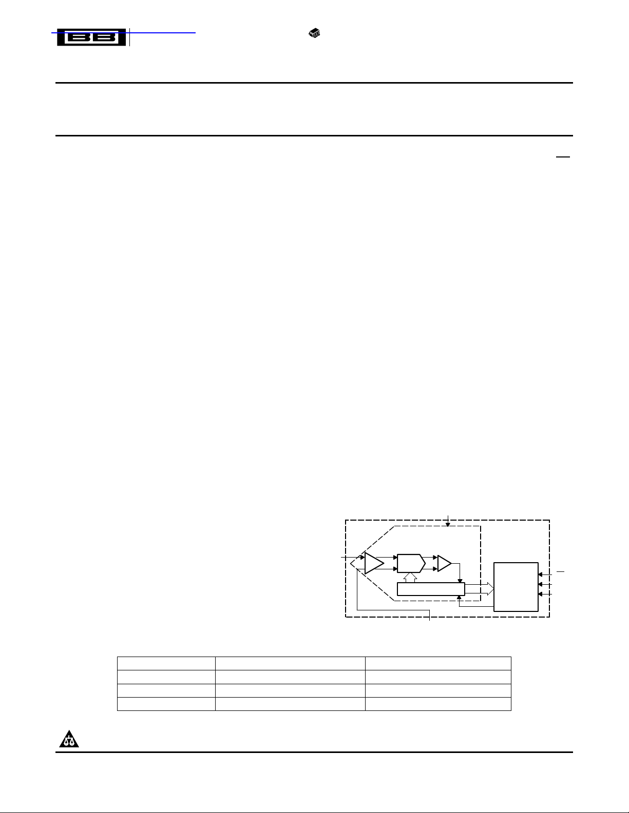
+
CDAC
SAR
Conversion
and
Control
Logic
Comparator
12/10/8 BIT ADC
VIN
REF/V
DD
CS
SCLK
SDO
GND
S/H
查询ADS7866IDBVR供应商
1.2-V, 12-/10-/8-BIT, 200-KSPS/100-KSPS, MICRO-POWER, MINIATURE
ANALOG-TO-DIGITAL CONVERTER WITH SERIAL INTERFACE
ADS7866
ADS7867
ADS7868
SLAS465 – JUNE 2005
FEATURES
• Single 1.2-V to 3.6-V Supply Operation
• High Throughput
– 200/240/280KSPS for 12/10/8-Bit V
– 100/120/140KSPS for 12/10/8-Bit V
• ± 1.5LSB INL, 12-Bit NMC (ADS7866)
• 71 dB SNR, –83 dB THD at fIN= 30 kHz
(ADS7866)
• Synchronized Conversion with SCLK
• SPI Compatible Serial Interface
• No Pipeline Delays
• Low Power
– 1.39 mW Typ at 200 KSPS, V
– 0.39 mW Typ at 200 KSPS, V
– 0.22 mW Typ at 100 KSPS, V
DD
DD
DD
• Auto Power-Down: 8 nA Typ, 300 nA Max
• 0 V to V
Unipolar Input Range
DD
• 6-Pin SOT-23 Package
APPLICATIONS
• Battery Powered Systems
• Isolated Data Acquisition
• Medical Instruments
• Portable Communication
• Portable Data Acquisition Systems
• Automatic Test Equipment
= 3.6 V
= 1.6 V
= 1.2 V
The sampling, conversion, and activation of digital
output SDO are initiated on the falling edge of CS.
The serial clock SCLK is used for controlling the
conversion rate and shifting data out of the converter.
≥ 1.6 V
DD
≥ 1.2 V
DD
Furthermore, SCLK provides a mechanism to allow
digital host processors to synchronize with the converter. These converters interface with
micro-processors or DSPs through a high-speed SPI
compatible serial interface. There are no pipeline
delays associated with the device.
The minimum conversion time is determined by the
frequency of the serial clock input, SCLK, while the
maximum frequency of SCLK is determined by the
minimum sampling time required to charge the input
capacitance to 12/10/8-bit accuracy for the
ADS7866/67/68, respectively. The maximum
throughput is determined by how often a conversion
is initiated when the minimum sampling time is met
and the maximum SCLK frequency is used. Each
device automatically powers down after each conversion, which allows each device to save power when
the throughput is reduced while using the maximum
SCLK frequency.
The converter reference is taken internally from the
supply. Hence, the analog input range for these
devices is 0 V to V
.
DD
These devices are available in a 6-pin SOT-23
package and are characterized over the industrial
–40 ° C to 85 ° C temperature range.
DESCRIPTION
The ADS7866/67/68 are low power, miniature,
12/10/8-bit A/D converters each with a unipolar,
single-ended input. These devices can operate from a
single 1.6 V to 3.6 V supply with a 200-KSPS
throughput for ADS7866. In addition, these devices
can maintain at least a 100-KSPS throughput with a
supply as low as 1.2 V.
Micro-Power Miniature SAR Converter Family
RESOLUTION/SPEED < 200 KSPS 1 MSPS – 1.25 MSPS
12-Bit ADS7866 (1.2 V
10-Bit ADS7867 (1.2 V
8-Bit ADS7868 (1.2 V
PRODUCTION DATA information is current as of publication date.
Products conform to specifications per the terms of the Texas
Instruments standard warranty. Production processing does not
necessarily include testing of all parameters.
Please be aware that an important notice concerning availability, standard warranty, and use in critical applications of Texas
Instruments semiconductor products and disclaimers thereto appears at the end of this data sheet.
to 3.6 VDD) ADS7886 (2.35 V
DD
to 3.6 VDD) ADS7887 (2.35 V
DD
to 3.6 VDD) ADS7888 (2.35 V
DD
to 5.25 VDD)
DD
to 5.25 VDD)
DD
to 5.25 VDD)
DD
Copyright © 2005, Texas Instruments Incorporated
Page 2
www.ti.com
ADS7866
ADS7867
ADS7868
SLAS465 – JUNE 2005
These devices have limited built-in ESD protection. The leads should be shorted together or the device
placed in conductive foam during storage or handling to prevent electrostatic damage to the MOS gates.
ORDERING INFORMATION
MAXIMUM MAXIMUM NO MISSING
MODEL MARKING TEMPERATURE MEDIA,
ADS7866I ± 1.5 –1/+1.5 12 SOT23-6 A66Y DBV –40 ° C to 85 ° C ADS7866IDBVT Small tape and reel, 250
ADS7866I ± 1.5 –1/+1.5 12 SOT23-6 A66Y DBV –40 ° C to 85 ° C ADS7866IDBVR Tape and reel, 3000
ADS7867I ± 0.5 ± 0.5 10 SOT23-6 A67Y DBV –40 ° C to 85 ° C ADS7867IDBVT Small tape and reel, 250
ADS7867I ± 0.5 ± 0.5 10 SOT23-6 A67Y DBV –40 ° C to 85 ° C ADS7867IDBVR Tape and reel, 3000
ADS7868I ± 0.5 ± 0.5 8 SOT23-6 A68Y DBV –40 ° C to 85 ° C ADS7868IDBVT Small tape and reel, 250
ADS7868I ± 0.5 ± 0.5 8 SOT23-6 A68Y DBV –40 ° C to 85 ° C ADS7868IDBVR Tape and reel, 3000
INTEGRAL DIFFERENTIAL CODES PACKAGE PACKAGE ORDERING
LINEARITY LINEARITY RESOLULTION TYPE DESIGNATOR NUMBER
(LSB) (LSB) (BIT)
PACKAGE SPECIFIED TRANSPORT
(SYMBOL) RANGE QUANTITY
(1)
(1) For the most current package and ordering information, see the Package Option Addendum at the end of this document, or see the TI
web site at www.ti.com.
ABSOLUTE MAXIMUM RATINGS
over operating free-air temperature range (unless otherwise noted)
RATING
V
to GND –0.3 V to 4.0 V
DD
Analog input voltage to GND –0.3 V to V
Digital input voltage to GND –0.3 V to 4.0 V
Digital output voltage to GND –0.3 V to V
T
A
T
STORAGE
T
J
Operating free-air temperature range –40 ° C to 85 ° C
Storage temperature range –65 ° C to 150 ° C
Junction temperature 150 ° C
SOT-23 Package
Lead temperature,
soldering
θJAThermal impedance 110.9 ° C/W
θJCThermal impedance 22.31 ° C/W
Vapor phase (10–40 sec) 250 ° C
Infrared (10–30 sec) 260 ° C
ESD 3 kV
+ 0.3 V
DD
+ 0.3 V
DD
2
Page 3

www.ti.com
ADS7866
ADS7867
ADS7868
SLAS465 – JUNE 2005
SPECIFICATIONS, ADS7866
At –40 ° C to 85 ° C, f
1.2 V ≤ V
SYSTEM PERFORMANCE
SAMPLING DYNAMICS (See Timing Characteristics Section)
t
CONVERT
t
SAMPLE
f
SAMPLE
DYNAMIC CHARACTERISTICS
SINAD dB
SNR Signal-to-noise ratio dB
THD Total harmonic distortion
SFDR dB
ANALOG INPUT
C
S
DIGITAL INPUT
V
IH
< 1.6 V (unless otherwise noted)
DD
PARAMETER TEST CONDITIONS MIN TYP MAX UNIT
Resolution 12 Bits
No missing codes 12 Bits
Integral linearity –1.5 1.5 LSB
Differential linearity –1 1.5 LSB
Offset error
Gain error
Total unadjusted error
Conversion time f
Acquisition time f
Throughput rate f
Aperture delay 10 ns
Aperture jitter 40 ps
Signal-to-noise
and distortion
Spurious free dynamic
range
Full-power bandwidth
Full-scale input span
Input capacitance 12 pF
Input leakage current –1 1 µA
Logic family , CMOS
Input logic high level V
(3)
SAMPLE
(2)
(7)
= 200 KSPS and f
1.2 V ≤ VDD< 1.6 V –2 2
1.6 V ≤ VDD≤ 3.6 V –3 3
1.2 V ≤ VDD< 1.6 V –2 2
1.6 V ≤ VDD≤ 3.6 V –2 2
1.2 V ≤ VDD< 1.6 V –2.5 2.5
(4)
1.6 V ≤ VDD≤ 3.6 V –3.5 3.5
= 3.4 MHz, 13 SCLK cycles 3.82 µs
SCLK
= 3.4 MHz, 1.6 V ≤ VDD≤ 3.6 V 0.64 µs
SCLK
= 3.4 MHz, 1.6 V ≤ VDD≤ 3.6 V 200 KSPS
SCLK
fIN= 30 kHz, 1.2 V ≤ VDD< 1.6 V 68
fIN= 30 kHz, 1.6 V ≤ VDD≤ 3.6 V 69 70
fIN= 30 kHz, 1.2 V ≤ VDD< 1.6 V 70
fIN= 30 kHz, 1.6 V ≤ VDD≤ 3.6 V 70 71
fIN= 30 kHz, 1.2 V ≤ VDD< 1.6 V –70
(5)
fIN= 30 kHz, 1.6 V ≤ VDD≤ 3.6 V –83
fIN= 30 kHz, 1.2 V ≤ VDD< 1.6 V 75
fIN= 30 kHz, 1.6 V ≤ VDD≤ 3.6 V 85
At 0.1 dB, 1.2 V ≤ VDD< 1.6 V 2
At 0.1 dB, 1.6 V ≤ VDD≤ 3.6 V 4
(6)
At 3 dB, 1.2 V ≤ VDD< 1.6 V 3
At 3 dB, 1.6 V ≤ VDD≤ 3.6 V 8
VIN – GND 0 V
1.2 V ≤ VDD< 1.6 V 0.7 × V
1.6 V ≤ VDD< 1.8 V 0.7 × V
1.8 V ≤ VDD< 2.5 V 0.7 × V
2.5 V ≤ VDD≤ 3.6 V 2 3.6
= 3.4 MHz if 1.6 V ≤ V
SCLK
≤ 3.6 V; f
DD
= 100 KSPS and f
SAMPLE
DD
DD
DD
SCLK
= 1.7 MHz if
DD
3.6
3.6
3.6
(1)
LSB
LSB
LSB
dB
MHz
V
(1) LSB = Least Significant BIt
(2) The difference in the first code transition 000...000 to 000...001 from the ideal value of GND + 1 LSB.
(3) The difference in the last code transition 011...111 to 111...111 from the ideal value of V
(4) The absolute difference from the ideal transfer function of the converter. This specification is similar to INL error except the effects of
- 1 LSB with the offset error removed.
DD
offset error and gain error are included.
(5) The 2nd through 10th harmonics are used to determine THD.
(6) Input frequency where the amplitude of the digitized signal has decreased by 0.1 dB or 3 dB.
(7) Ideal input span which does not include gain or offset errors.
3
Page 4

www.ti.com
ADS7866
ADS7867
ADS7868
SLAS465 – JUNE 2005
SPECIFICATIONS, ADS7866 (continued)
At –40 ° C to 85 ° C, f
1.2 V ≤ V
V
IL
I
SCLK
I
CS
C
IN
DIGITAL OUTPUT
V
OH
V
OL
I
SDO
C
OUT
POWER SUPPLY REQUIREMENTS
V
DD
I
DD
I
DD
POWER DISSIPATION
TEMPERATURE RANGE
DD
PARAMETER TEST CONDITIONS MIN TYP MAX UNIT
Input logic low level V
SCLK pin leakage current Digital input = 0 V or V
CS pin leakage current ± 1 µA
Digital input pin capacitance 10 pF
Output logic high level I
Output logic low level I
SDO pin leakage current Floating output –1 1 µA
Digital output pin
capacitance
Data format, straight binary
Supply voltage 1.2 3.6 V
Supply current, Digital inputs = 0 V
normal operation or V
Power-down mode SCLK on or off 0.008 0.3 µA
Normal operation f
Power-down mode SCLK on or off, VDD= 3.6 V 1.08 µW
Specified performance –40 85 ° C
SAMPLE
< 1.6 V (unless otherwise noted)
= 200 KSPS and f
= 3.4 MHz if 1.6 V ≤ V
SCLK
≤ 3.6 V; f
DD
= 100 KSPS and f
SAMPLE
1.2 V ≤ VDD< 1.6 V –0.2 0.2 × V
1.6 V ≤ VDD< 1.8 V –0.2 0.2 × V
1.8 V ≤ VDD< 2.5 V –0.2 0.3 × V
2.5 V ≤ VDD≤ 3.6 V –0.2 0.8
DD
= 200 µA VDD–0.2 V
SOURCE
= 200 µA 0 0.2 V
SINK
–1 0.02 1 µA
Floating output 10 pF
f
f
SAMPLE
SAMPLE
f
SAMPLE
DD
= 200 KSPS, f
= 200 KSPS, f
= 100 KSPS, f
= 200 KSPS, f
SAMPLE
f
= 100 KSPS, f
SAMPLE
f
= 50 KSPS, f
SAMPLE
f
= 20 KSPS, f
SAMPLE
f
= 200 KSPS, f
SAMPLE
f
= 100 KSPS, f
SAMPLE
f
= 50 KSPS, f
SAMPLE
f
= 20 KSPS, f
SAMPLE
f
= 200 KSPS, f
SAMPLE
f
= 100 KSPS, f
SAMPLE
f
= 50 KSPS, f
SAMPLE
f
= 20 KSPS, f
SAMPLE
f
= 200 KSPS, f
SAMPLE
f
= 100 KSPS, f
SAMPLE
f
= 50 KSPS, f
SAMPLE
f
= 20 KSPS, f
SAMPLE
f
= 200 KSPS, f
SAMPLE
f
= 100 KSPS, f
SAMPLE
f
= 50 KSPS, f
SAMPLE
f
= 20 KSPS, f
SAMPLE
f
= 100 KSPS, f
SAMPLE
f
= 50 KSPS, f
SAMPLE
f
= 20 KSPS, f
SAMPLE
= 3.4 MHz, VDD= 3.6 V 1.39 1.80
SCLK
= 3.4 MHz, VDD= 1.6 V 0.39 0.53 mW
SCLK
= 1.7 MHz, VDD= 1.2 V 0.22 0.3
SCLK
= 3.4 MHz, VDD= 3.6 V 385 500
SCLK
= 3.4 MHz, VDD= 3.6 V 193
SCLK
= 3.4 MHz, VDD= 3.6 V 97
SCLK
= 3.4 MHz, VDD= 3.6 V 39
SCLK
= 3.4 MHz, VDD= 3 V 340
SCLK
= 3.4 MHz, VDD= 3 V 170
SCLK
= 3.4 MHz, VDD= 3 V 85
SCLK
= 3.4 MHz, VDD= 3 V 35
SCLK
= 3.4 MHz, VDD= 2.5 V 305
SCLK
= 3.4 MHz, VDD= 2.5 V 153
SCLK
= 3.4 MHz, VDD= 2.5 V 77
SCLK
= 3.4 MHz, VDD= 2.5 V 31
SCLK
= 3.4 MHz, VDD= 1.8 V 256
SCLK
= 3.4 MHz, VDD= 1.8 V 128
SCLK
= 3.4 MHz, VDD= 1.8 V 65
SCLK
= 3.4 MHz, VDD= 1.8 V 26
SCLK
= 3.4 MHz, VDD= 1.6 V 241 330
SCLK
= 3.4 MHz, VDD= 1.6 V 121
SCLK
= 3.4 MHz, VDD= 1.6 V 61
SCLK
= 3.4 MHz, VDD= 1.6 V 25
SCLK
= 1.7 MHz, VDD= 1.2 V 186 250
SCLK
= 1.7 MHz, VDD= 1.2 V 93 µA
SCLK
= 1.7 MHz, VDD= 1.2 V 37
SCLK
SCLK
= 1.7 MHz if
DD
DD
DD
DD
V
µA
µA
µA
µA
µA
4
Page 5

www.ti.com
ADS7866
ADS7867
ADS7868
SLAS465 – JUNE 2005
SPECIFICATIONS, ADS7867
At –40 ° C to 85 ° C, f
1.2 V ≤ V
SYSTEM PERFORMANCE
SAMPLING DYNAMICS (See Timing Characteristics Section)
t
CONVERT
t
SAMPLE
f
SAMPLE
DYNAMIC CHARACTERISTICS
SINAD dB
SNR Signal-to-noise ratio dB
THD Total harmonic distortion
SFDR Spurious free dynamic range dB
ANALOG INPUT
C
S
DIGITAL INPUT
V
IH
< 1.6 V (unless otherwise noted)
DD
PARAMETER TEST CONDITIONS MIN TYP MAX UNIT
Resolution 10 Bits
No missing codes 10 Bits
Integral linearity –0.5 0.5 LSB
Differential linearity –0.5 0.5 LSB
Offset error
Gain error
(3)
Total unadjusted error
Conversion time f
Acquisition time f
Throughput rate f
Aperture delay 10 ns
Aperture jitter 40 ps
Signal-to-noise
and distortion
Full-power bandwidth
Full-scale input span
Input capacitance 12 pF
Input leakage current –1 1 µA
Logic family, CMOS
Input logic high level V
= 240 KSPS and f
SAMPLE
(2)
(7)
= 3.4 MHz if 1.6 V ≤ V
SCLK
≤ 3.6 V; f
DD
= 120 KSPS and f
SAMPLE
1.2 V ≤ VDD< 1.6 V –0.75 0.75
1.6 V ≤ VDD≤ 3.6 V –1 1
1.2 V ≤ VDD< 1.6 V –0.5 0.5
1.6 V ≤ VDD≤ 3.6 V –0.5 0.5
1.2 V ≤ VDD< 1.6 V –2 2
(4)
1.6 V ≤ VDD≤ 3.6 V –2 2
= 3.4 MHz, 11 SCLK cycles 3.235 µs
SCLK
= 3.4 MHz, 1.6 V ≤ VDD≤ 3.6 V 0.64 µs
SCLK
= 3.4 MHz, 1.6 V ≤ VDD≤ 3.6 V 240 KSPS
SCLK
f
= 100 KSPS, fIN= 30 kHz, 1.2 V ≤ VDD< 1.6 V 61
SAMPLE
f
= 200 KSPS, fIN= 30 kHz, 1.6 V ≤ VDD≤ 3.6 V 61 61.7
SAMPLE
f
= 100 KSPS, fIN= 30 kHz, 1.2 V ≤ VDD< 1.6 V 61.5
SAMPLE
f
= 200 KSPS, fIN= 30 kHz, 1.6 V ≤ VDD≤ 3.6 V 61.8
SAMPLE
f
= 100 KSPS, fIN= 30 kHz, 1.2 V ≤ VDD< 1.6 V -68
SAMPLE
(5)
f
= 200 KSPS, fIN= 30 kHz, 1.6 V ≤ VDD≤ 3.6 V -78 -72
SAMPLE
f
= 100 KSPS, fIN= 30 kHz, 1.2 V ≤ VDD< 1.6 V 73
SAMPLE
f
= 200 KSPS, fIN= 30 kHz, 1.6 V ≤ VDD≤ 3.6 V 74 80
SAMPLE
At 0.1 dB, 1.2 V ≤ VDD< 1.6 V 2
At 0.1 dB, 1.6 V ≤ VDD≤ 3.6 V 4
(6)
At 3 dB, 1.2 V ≤ VDD< 1.6 V 3
At 3 dB, 1.6 V ≤ VDD≤ 3.6 V 8
VIN – GND 0 V
1.2 V ≤ VDD< 1.6 V 0.7 × V
1.6 V ≤ VDD< 1.8 V 0.7 × V
1.8 V ≤ VDD< 2.5 V 0.7 × V
2.5 V ≤ VDD≤ 3.6 V 2 3.6
= 1.7 MHz if
SCLK
DD
DD
DD
DD
3.6
3.6
3.6
(1)
LSB
LSB
LSB
dB
MHz
V
(1) LSB = Least Significant BIt
(2) The difference in the first code transition 000...000 to 000...001 from the ideal value of GND + 1 LSB.
(3) The difference in the last code transition 011...111 to 111...111 from the ideal value of V
(4) The absolute difference from the ideal transfer function of the converter. This specification is similar to INL error except the effects of
- 1 LSB with the offset error removed.
DD
offset error and gain error are included.
(5) The 2nd through 10th harmonics are used to determine THD.
(6) Input frequency where the amplitude of the digitized signal has decreased by 0.1 dB or 3 dB.
(7) Ideal input span which does not include gain or offset errors.
5
Page 6
www.ti.com
ADS7866
ADS7867
ADS7868
SLAS465 – JUNE 2005
SPECIFICATIONS, ADS7867 (continued)
At –40 ° C to 85 ° C, f
1.2 V ≤ V
V
IL
I
SCLK
I
CS
C
IN
DIGITAL OUTPUT
V
OH
V
OL
I
SDO
C
OUT
POWER SUPPLY REQUIREMENTS
V
DD
I
DD
I
DD
POWER DISSIPATION
TEMPERATURE RANGE
DD
PARAMETER TEST CONDITIONS MIN TYP MAX UNIT
Input logic low level V
SCLK pin leakage current Digital input = 0 V or V
CS pin leakage current ± 1 µA
Digital input pin capacitance 10 pF
Output logic high level I
Output logic low level I
SDO pin leakage current Floating output –1 1 µA
Digital output pin
capacitance
Data format, straight binary
Supply voltage 1.2 3.6 V
Supply current, Digital Inputs = 0 V
normal operation or V
Power-down mode SCLK on or off 0.008 0.3 µA
Normal operation f
Power-down mode SCLK on or off, VDD= 3.6 V 1.08 µW
Specified performance –40 85 ° C
SAMPLE
< 1.6 V (unless otherwise noted)
= 240 KSPS and f
1.2 V ≤ VDD< 1.6 V –0.2 0.2 × V
1.6 V ≤ VDD< 1.8 V –0.2 0.2 × V
1.8 V ≤ VDD< 2.5 V –0.2 0.3 × V
2.5 V ≤ VDD≤ 3.6 V –0.2 0.8
= 200 µA VDD–0.2 V
SOURCE
= 200 µA 0 0.2 V
SINK
Floating output 10 pF
DD
f
= 240 KSPS, f
SAMPLE
= 240 KSPS, f
SAMPLE
f
= 120 KSPS, f
SAMPLE
= 3.4 MHz if 1.6 V ≤ V
SCLK
DD
f
= 240 KSPS, f
SAMPLE
f
= 100 KSPS, f
SAMPLE
f
= 240 KSPS, f
SAMPLE
f
= 100 KSPS, f
SAMPLE
f
= 120 KSPS, f
SAMPLE
f
= 50 KSPS, f
SAMPLE
= 3.4 MHz, VDD= 3.6 V 1.51 1.80
SCLK
= 3.4 MHz, VDD= 1.6 V 0.42 0.53 mW
SCLK
= 1.7 MHz, VDD= 1.2 V 0.24 0.30
SCLK
≤ 3.6 V; f
DD
= 120 KSPS and f
SAMPLE
–1 0.02 1 µA
= 3.4 MHz, VDD= 3.6 V 420 500
SCLK
= 3.4 MHz, VDD= 3.6 V 172
SCLK
= 3.4 MHz, VDD= 1.6 V 261 330
SCLK
= 3.4 MHz, VDD= 1.6 V 107
SCLK
= 1.7 MHz, VDD= 1.2 V 202 250
SCLK
= 1.7 MHz, VDD= 1.2 V 83
SCLK
SCLK
= 1.7 MHz if
DD
DD
DD
DD
V
µA
µA
µA
6
Page 7
www.ti.com
ADS7866
ADS7867
ADS7868
SLAS465 – JUNE 2005
SPECIFICATIONS, ADS7868
At –40 ° C to 85 ° C, f
1.2 V ≤ V
SYSTEM PERFORMANCE
SAMPLING DYNAMICS (See Timing Characteristics Section)
t
CONVERT
t
SAMPLE
f
SAMPLE
DYNAMIC CHARACTERISTICS
SINAD dB
SNR Signal-to-noise ratio dB
THD dB
SFDR dB
ANALOG INPUT
C
S
DIGITAL INPUT
V
IH
< 1.6 V (unless otherwise noted)
DD
PARAMETER TEST CONDITIONS MIN TYP MAX UNIT
Resolution 8 Bits
No missing codes 8 Bits
Integral linearity –0.5 0.5 LSB
Differential linearity –0.5 0.5 LSB
Offset error
Gain error
(3)
Total unadjusted error
Conversion time f
Acquisition time f
Throughput rate f
Aperture delay 10 ns
Aperture jitter 40 ps
Signal-to-noise
and distortion
Total harmonic
(5)
distortion
Spurious free dynamic
range
Full-power bandwidth
Full-scale input span
Input capacitance 12 pF
Input leakage current –1 1 µA
Logic family, CMOS
Input logic high level V
= 280 KSPS and f
SAMPLE
(2)
(7)
= 3.4 MHz if 1.6 V ≤ V
SCLK
≤ 3.6 V; f
DD
= 140 KSPS and f
SAMPLE
1.2 V ≤ VDD< 1.6 V –0.5 0.5
1.6 V ≤ VDD≤ 3.6 V –0.5 0.5
1.2 V ≤ VDD< 1.6 V –0.5 0.5
1.6 V ≤ VDD≤ 3.6 V –0.5 0.5
1.2 V ≤ VDD< 1.6 V –1 1
(4)
1.6 V ≤ VDD≤ 3.6 V –1 1
= 3.4 MHz, 9 SCLK cycles 2.647 µs
SCLK
= 3.4 MHz, 1.6 V ≤ VDD≤ 3.6 V 0.64 µs
SCLK
= 3.4 MHz, 1.6 V ≤ VDD≤ 3.6 V 280 KSPS
SCLK
f
= 100 KSPS, fIN= 30 kHz, 1.2 V ≤ VDD< 1.6 V 49
SAMPLE
f
= 200 KSPS, fIN= 30 kHz, 1.6 V ≤ VDD≤ 3.6 V 49 49.4
SAMPLE
f
= 100 KSPS, fIN= 30 kHz, 1.2 V ≤ VDD< 1.6 V 49.4
SAMPLE
f
= 200 KSPS, fIN= 30 kHz, 1.6 V ≤ VDD≤ 3.6 V 49.8
SAMPLE
f
= 100 KSPS, fIN= 30 kHz, 1.2 V ≤ VDD< 1.6 V –65
SAMPLE
f
= 200 KSPS, fIN= 30 kHz, 1.6 V ≤ VDD≤ 3.6 V –72 -66
SAMPLE
f
= 100 KSPS, fIN= 30 kHz, 1.2 V ≤ VDD< 1.6 V 67
SAMPLE
f
= 200 KSPS, fIN= 30 kHz, 1.6 V ≤ VDD≤ 3.6 V 66 67
SAMPLE
At 0.1 dB, 1.2 V ≤ VDD< 1.6 V 2
At 0.1 dB, 1.6 V ≤ VDD≤ 3.6 V 4
(6)
At 3 dB, 1.2 V ≤ VDD< 1.6 V 3
At 3 dB, 1.6 V ≤ VDD≤ 3.6 V 8
VIN – GND 0 V
1.2 V ≤ VDD< 1.6 V 0.7 × V
1.6 V ≤ VDD< 1.8 V 0.7 × V
1.8 V ≤ VDD< 2.5 V 0.7 × V
DD
DD
DD
2.5 V ≤ VDD≤ 3.6 V 2 3.6
SCLK
= 1.7 MHz if
DD
3.6
3.6
3.6
(1)
LSB
LSB
LSB
MHz
V
(1) LSB = Least Significant BIt
(2) The difference in the first code transition 000...000 to 000...001 from the ideal value of GND + 1 LSB.
(3) The difference in the last code transition 011...111 to 111...111 from the ideal value of V
(4) The absolute difference from the ideal transfer function of the converter. This specification is similar to INL error except the effects of
- 1 LSB with the offset error removed.
DD
offset error and gain error are included.
(5) The 2nd through 10th harmonics are used to determine THD.
(6) Input frequency where the amplitude of the digitized signal has decreased by 0.1 dB or 3 dB.
(7) Ideal input span which does not include gain or offset errors.
7
Page 8
www.ti.com
ADS7866
ADS7867
ADS7868
SLAS465 – JUNE 2005
SPECIFICATIONS, ADS7868 (continued)
At –40 ° C to 85 ° C, f
1.2 V ≤ V
V
IL
I
SCLK
I
CS
C
IN
DIGITAL OUTPUT
V
OH
V
OL
I
SDO
C
OUT
POWER SUPPLY REQUIREMENTS
V
DD
I
DD
I
DD
POWER DISSIPATION
TEMPERATURE RANGE
DD
PARAMETER TEST CONDITIONS MIN TYP MAX UNIT
Input logic low level V
SCLK pin leakage current Digital input = 0 V or V
CS pin leakage current ± 1 µA
Digital input pin
capacitance
Output logic high level I
Output logic low level I
SDO pin leakage current Floating output –1 1 µA
Digital output pin
capacitance
Data format, straight
binary
Supply voltage 1.2 3.6 V
Supply current, Digital Inputs = 0 V
normal operation or V
Power-down mode SCLK on or off 0.008 0.3 µA
Normal operation f
Power-down mode SCLK on or off, VDD= 3.6 V 1.08 µW
Specified performance –40 85 ° C
SAMPLE
< 1.6 V (unless otherwise noted)
= 280 KSPS and f
= 3.4 MHz if 1.6 V ≤ V
SCLK
≤ 3.6 V; f
DD
= 140 KSPS and f
SAMPLE
1.2 V ≤ VDD< 1.6 V –0.2 0.2 × V
1.6 V ≤ VDD< 1.8 V –0.2 0.2 × V
1.8 V ≤ VDD< 2.5 V –0.2 0.3 × V
2.5 V ≤ VDD≤ 3.6 V –0.2 0.8
DD
= 200 µA VDD–0.2 V
SOURCE
= 200 µA 0 0.2 V
SINK
–1 0.02 1 µA
Floating output 10 pF
f
f
SAMPLE
SAMPLE
f
SAMPLE
DD
= 280 KSPS, f
= 280 KSPS, f
= 140 KSPS, f
= 280 KSPS, f
SAMPLE
f
= 100 KSPS, f
SAMPLE
f
= 280 KSPS, f
SAMPLE
f
= 100 KSPS, f
SAMPLE
f
= 140 KSPS, f
SAMPLE
f
= 50 KSPS, f
SAMPLE
= 3.4 MHz, VDD= 3.6 V 1.58 1.8
SCLK
= 3.4 MHz, VDD= 1.6 V 0.42 0.53 mW
SCLK
= 1.7 MHz, VDD= 1.2 V 0.24 0.3
SCLK
= 3.4 MHz, VDD= 3.6 V 439 500
SCLK
= 3.4 MHz, VDD= 3.6 V 154
SCLK
= 3.4 MHz, VDD= 1.6 V 264 330
SCLK
= 3.4 MHz, VDD= 1.6 V 93
SCLK
= 1.7 MHz, VDD= 1.2 V 201 250
SCLK
= 1.7 MHz, VDD= 1.2 V 70
SCLK
SCLK
= 1.7 MHz if
DD
DD
DD
10 pF
DD
V
µA
µA
µA
8
Page 9

www.ti.com
TIMING REQUIREMENTS
1
2
354
6
10
16
14
12
1
9
SCLK
SDO
Hi−Z
Auto Power−Down
7
8
Last SCLK= 16for ADS7866
14for ADS 7867
12for ADS 7868
Hi−Z
Auto Power−Down
2
t
SU(CSF−FSCLKF)
t
C(SCLK)
t
WH(SCLK)
t
WL(SCLK)
t
WH(CS)
t
SU(LSBZ−CSF)
t
DIS(EOC−SDOZ)
t
SU(CSF−FSCLKF)
t
D(CSF−SDOVALID)
“0” “0” “0”
t
CONVERT
“0” “0” “0”
t
H(SCLKF−SDOVALID)
t
D(SCLKF−SDOVALID)
t
D(CSF−SDOVALID)
t
SAMPLE
“0”
HOLD EOC
CS
t
CYCLE
MSB MSB−1 MSB−2 MSB−3 MSB−4 MSB−5
LSB
At –40°C to 85°C, f
= 3.4 MHz if 1.6 V ≤ V
SCLK
(1) (2)
≤ 3.6 V; f
DD
= 1.7 MHz if 1.2 V ≤ V
SCLK
< 1.6 V, 50-pF Load on SDO Pin,
DD
unless otherwise noted
PARAMETER TEST CONDITIONS MIN TYP MAX UNIT
t
sample
t
convert
t
C(SCLK)
t
WH(SCLK)
t
WL(SCLK)
t
SU(CSF-FSCLKF)
t
D(CSF-SDOVALID)
t
H(SCLKF-SDOVALID)
t
D(SCLKF-SDOVALID)
t
DIS(EOC-SDOZ)
t
WH(CS)
t
SU(LSBZ-CSF)
(1) All input signals are specified with tr= tf= 5 ns (10% to 90% of VDD) and timed from a voltage level of (V
(2) See timing diagram in Figure 1 .
(3) Min t
Total Cycle Time section for further details.
Sample time t
SU(CSF-FSCLKF)
+ 2 × t
ADS7866 13 × t
Conversion time ADS7867 11 × t
ADS7868 9 × t
1.2 V ≤ VDD< 1.6 V See
Cycle time µs
1.6 V ≤ VDD< 1.8 V See
1.8 V ≤ VDD< 2.5 V See
2.5 V ≤ VDD≤ 3.6 V See
Pulse duration 0.4 × t
Pulse duration 0.4 × t
(3)
(3)
(3)
(3)
C(SCLK)
C(SCLK)
1.2 V ≤ VDD< 1.6 V 192
Setup time 1.6 V ≤ VDD< 1.8 V 55 ns
1.8 V ≤ VDD≤ 3.6 V 55
1.2 V ≤ VDD< 1.6 V 65
Delay time 1.6 V ≤ VDD< 1.8 V 55 ns
1.8 V ≤ VDD≤ 3.6 V 55
1.2 V ≤ VDD< 1.6 V 20
Hold time 1.6 V ≤ VDD< 1.8 V 10 ns
1.8 V ≤ VDD≤ 3.6 V 10
1.2 V ≤ VDD< 1.6 V 140
Delay time 1.6 V ≤ VDD< 1.8 V 140 ns
1.8 V ≤ VDD≤ 3.6 V 140
1.2 V ≤ VDD< 1.6 V 10 80
Disable time 1.6 V ≤ VDD< 1.8 V 7 60 ns
1.8 V ≤ VDD≤ 3.6 V 7 60
1.2 V ≤ VDD< 1.6 V 20
Pulse duration 1.6 V ≤ VDD< 1.8 V 10 ns
1.8 V ≤ VDD≤ 3.6 V 10
1.2 V ≤ VDD< 1.6 V 20
Setup time 1.6 V ≤ VDD< 1.8 V 10 ns
1.8 V ≤ VDD≤ 3.6 V 10
is determined by the Min t
C(SCLK)
of the specific resolution and supply voltage. See Acquisition Time, Conversion Time, and
SAMPLE
ADS7866
ADS7867
ADS7868
SLAS465 – JUNE 2005
C(SCLK)
C(SCLK)
C(SCLK)
C(SCLK)
100
100
50
6.7
0.6 × t
C(SCLK)
0.6 × t
C(SCLK)
+ VIH)/2.
IL
µs
µs
ns
ns
Figure 1. Timing Diagram
9
Page 10

www.ti.com
3
2
4
6
(TOP VIEW)
1
REF/V
DD
GND
VIN
SCLK
ADS7866/67/68
DBV PACKAGE
CS
5
SDO
ADS7866
ADS7867
ADS7868
SLAS465 – JUNE 2005
PIN CONFIGURATION
TERMINAL FUNCTIONS
TERMINAL
NAME NO.
REF/V
DD
GND 2 Ground for signal and power supply. All analog and digital signals are referred with respect to this pin.
VIN 3 Analog signal input
SCLK 4 Serial clock input. This clock is used for clocking data out, and it is the source of conversion clock.
SDO 5
CS 6
1 External reference input and power supply
This is the serial data output of the conversion result. The serial stream comes with MSB first. The MSB is clocked out
(changed) on the falling edge one SCLK after the sampling period ends. This results in four leading zeros after CS
becomes active. SDO is 3-stated once all the valid bits are clocked out (12 for ADS7866, 10 for ADS7867, and 8 for
ADS7868).
This is an active low input signal. It is used as a chip select to gate the SCLK input, to initiate a conversion, and to
frame output data.
DESCRIPTION
10
Page 11

www.ti.com
TYPICAL CHARACTERISTICS ADS7866
−100
−90
−80
−70
−60
−50
−40
−30
−20
−10
0
0 10 20 30 40 50 60 70 80 90 100
fi − Input Frquency − kHz
Normalized Amplitude − dB
VDD = 1.6 V ,
f
SAMPLE
= 200 kSPS,
fi = 30 kHz,
SNR = 72.31 dB,
SINAD = 71.97 dB,
THD (9) = −83.18 dB,
SFDR = 86.83 dB
−100
−90
−80
−70
−60
−50
−40
−30
−20
−10
0
0 5 10 15 20 25 30 35 40 45 50
fi − Input Frquency − kHz
Normalized Amplitude − dB
VDD = 1.2 V ,
f
SAMPLE
= 100 kSPS,
fi = 30 kHz,
SNR = 71.42 dB,
SINAD = 67.62 dB,
THD (9) = −69.96 dB,
SFDR = 75.14 dB
−82
−80
−78
−76
−74
−72
−70
−68
−66
−64
−62
−60
−58
−56
1
10
100
1000
VDD = 3.6V,
200 KSPS
VDD = 2.5 V,
200 KSPS
VDD = 1.6 V, 200 KSPS
VDD = 1.2 V,
100 KSPS
THD Using 2nd − 10th harmonics,
TA = 25°C
fi − Input Frequency − kHz
THD − Total Harmonic Distortion − dB
67
67.5
68
68.5
69
69.5
70
70.5
71
71.5
72
72.5
73
1 10 100 1000
VDD = 3.6 V,
200 KSPS
VDD = 2.5 V, 200 KSPS
VDD = 1.6 V,
200 KSPS
VDD = 1.2 V,
100 KSPS
fi − Input Frequency − kHz
SNR − Signal-to-Noise Ratio − dB
57
59
61
63
65
67
69
71
73
1
10
100
1000
VDD = 3.6 V, 200 KSPS
fi − Input Frequency − kHz
VDD = 2.5 V,
200 KSPS
VDD = 1.6 V,
200 KSPS
VDD = 1.2 V,
100 KSPS
SINAD − Signal-to-Noise and Distortion − dB
FFT (8192 Points)
Figure 2.
FFT (8192 Points)
ADS7866
ADS7867
ADS7868
SLAS465 – JUNE 2005
SIGNAL-TO-NOISE RATIO SIGNAL-TO-NOISE TOTAL HARMONIC DISTORTION
INPUT FREQUENCY vs INPUT FREQUENCY
Figure 3.
vs AND DISTORTION vs
INPUT FREQUENCY
Figure 4. Figure 5. Figure 6.
11
Page 12

www.ti.com
62
64
66
68
70
72
74
76
78
80
82
84
1
10
100
1000
VDD = 3.6V,
200 KSPS
VDD = 2.5V,
200 KSPS
VDD = 1.6 V,
200 KSPS
VDD = 1.2 V, 100 KSPS
fi − Input Frequency − kHz
SFDR − Spurious Free Dynamic Range − dB
100
125
150
175
200
225
250
275
300
325
1.6 1.8 2 2.2 2.4 2.6 2.8 3 3.2 3.4
VDD = 3.6 V
VDD = 3 V
VDD = 2.5 V
VDD = 1.8 V
VDD = 1.6 V
TA = 25°C,
f
SAMPLE
= 100 KSPS
SCLK Frequency − MHz
CC
I Supply Current − − Aµ
200
225
250
275
300
325
350
375
400
425
1.6 1.8 2 2.2 2.4 2.6 2.8 3 3.2 3.4 3.6
TA = −40C
TA = 25C
TA = 85C
VDD − Supply Voltage − V
CC
I Supply Current − − Aµ
f
SAMPLE
= 200 KSPS,
f
SCLK
= 3.4 MHz
0
0.2
0.4
0.6
0.8
1
1.2
1.4
20 40 60 80 100 120 140 160 180 200
VDD = 3.6 V
VDD = 3 V
VDD = 2.5 V
VDD = 1.8 V
VDD = 1.6 V
Throughput − KSPS
Power Consumption − mW
TA = 25°C,
SCLK = 3.4 MHz
−84
−82
−80
−78
−76
−74
−72
−70
−68
−66
−64
−62
−60
−58
1 10 100 1000
RI = 0
RI = 1000
RI = 500
RI = 100
RI = 10
VDD = 1.6 V,
TA = 25°C,
f
SAMPLE
= 200 KSPS,
f
SCLK
= 3.4 MHz
fi − Input Frequency − kHz
THD − Total Harmonic Distortion − dB
−1
−0.8
−0.6
−0.4
−0.2
0
0.2
0.4
0.6
0.8
1
0 512 1024 1536 2048 2560 3072 3584 4096
VDD = 1.6 V ,
TA = 25°C,
f
SAMPLE
= 200 KSPS,
f
SCLK
= 3.4 MHz
Code
INL − LSBs
(Straight Binary in Decimal)
ADS7866
ADS7867
ADS7868
SLAS465 – JUNE 2005
TYPICAL CHARACTERISTICS ADS7866 (continued)
SPURIOUS FREE DYNAMIC RANGE SUPPLY CURRENT SUPPLY CURRENT
vs vs vs
INPUT FREQUENCY SCLK FREQUENCY SUPPLY VOLTAGE
Figure 7. Figure 8. Figure 9.
POWER CONSUMPTION TOTAL HARMONIC DISTORTION
vs vs
THROUGHPUT INPUT FREQUENCY
12
Figure 10. Figure 11.
INL
Figure 12.
Page 13

www.ti.com
−0.8
−0.6
−0.4
−0.2
0
0.2
0.4
0.6
0.8
1
0 512 1024 1536 2048 2560 3072 3584 4096
VDD = 1.6 V ,
TA = 25°C,
f
SAMPLE
= 200 KSPS,
f
SCLK
= 3.4 MHz
Code
DNL − LSBs
(Straight Binary in Decimal)
−1
−0.8
−0.6
−0.4
−0.2
0
0.2
0.4
0.6
0.8
1
0 512 1024 1536 2048 2560 3072 3584 4096
VDD = 1.2 V ,
TA = 25°C,
f
SAMPLE
= 100 KSPS,
f
SCLK
= 1.7 MHz
Code
INL − LSBs
(Straight Binary in Decimal)
−0.8
−0.6
−0.4
−0.2
0
0.2
0.4
0.6
0.8
1
0 512 1024 1536 2048 2560 3072 3584 4096
VDD = 1.2 V ,
TA = 25°C,
f
SAMPLE
= 100 KSPS,
f
SCLK
= 1.7 MHz
Code
DNL − LSBs
(Straight Binary in Decimal)
TYPICAL CHARACTERISTICS ADS7866 (continued)
ADS7866
ADS7867
ADS7868
SLAS465 – JUNE 2005
DNL
Figure 13.
INL
Figure 14.
DNL
Figure 15.
13
Page 14

www.ti.com
200
225
250
275
300
325
350
375
400
425
1.2 1.4 1.6 1.8 2 2.2 2.4 2.6 2.8 3 3.2 3.4 3.6
f
SCLK
= 3.4 MHz
f
SCLK
= 2.4 MHz
f
SCLK
= 1.7 MHz
TA = 25°C,
f
SAMPLE
= (f
SCLK
)/16
VDD − Supply Voltage − V
CC
I Supply Current − − Aµ
150
175
200
225
250
275
300
1.2 1.4 1.6 1.8
VDD − Supply Voltage − V
Throughput Rate − KSPS
12-Bit NMC, TA = 25°C,
t
SAMPLE
= 2.375/f
SCLK
,
t
DIS(EOC-SDOZ)+tSU(LSBZ-CSF)
= 0.375/f
SCLK
,
Throughput Rate = 16 SCLK Cycles
250
275
300
325
350
375
400
425
450
1.6 1.8 2 2.2 2.4 2.6 2.8 3 3.2 3.4 3.6
VDD − Supply Voltage − V
Throughput Rate − KSPS
12-Bit NMC, TA = 25°C,
t
SAMPLE
= 2.25/f
SCLK
,
t
DIS(EOC-SDOZ)+tSU(LSBZ-CSF)
= 0.25/f
SCLK
,
Throughput Rate = 16 SCLK Cycles
ADS7866
ADS7867
ADS7868
SLAS465 – JUNE 2005
TYPICAL CHARACTERISTICS ADS7866 (continued)
MAX SUPPLY CURRENT THROUGHPUT RATE THROUGHPUT RATE
vs vs vs
SUPPLY VOLTAGE SUPPLY VOLTAGE SUPPLY VOLTAGE
Figure 16. Figure 17. Figure 18.
14
Page 15

www.ti.com
TYPICAL CHARACTERISTICS ADS7867
−100
−90
−80
−70
−60
−50
−40
−30
−20
−10
0
0 5 10 15 20 25 30 35 40 45 50
VDD = 1.2 V ,
f
SAMPLE
= 100 KSPS,
fi = 30 kHz,
SNR = 60.419 dB,
SINAD = 59.877 dB,
THD (9) = −69.181 dB,
SFDR = 73.682 dB
fi − Input Frequency − kHz
Normalized Amplitude − dB
−100
−90
−80
−70
−60
−50
−40
−30
−20
−10
0
0 10 20 30 40 50 60 70 80 90 100
Normalized Amplitude − dB
VDD = 1.6 V ,
f
SAMPLE
= 200 KSPS,
fi = 30 kHz,
SNR = 61.173 dB,
SINAD = 61.128 dB,
THD (9) = −80.986 dB,
SFDR = 83.468 dB
fi − Input Frequency − kHz
250
275
300
325
350
375
400
425
450
1.6 1.8 2 2.2 2.4 2.6 2.8 3 3.2 3.4 3.6
VDD − Supply Voltage − V
Throughput Rate − KSPS
10-Bit NMC, TA = 25°C,
t
SAMPLE
= 2.25/f
SCLK
,
t
DIS(EOC-SDOZ)+tSU(LSBZ-CSF)
= 0.25/f
SCLK
,
Throughput Rate = 14 SCLK Cycles
150
175
200
225
250
275
1.2 1.4 1.6 1.8
VDD − Supply Voltage − V
Throughput Rate − KSPS
10-Bit NMC, TA = 25°C,
t
SAMPLE
= 2.375/f
SCLK
,
t
DIS(EOC-SDOZ)+tSU(LSBZ-CSF)
= 0.375/f
SCLK
,
Throughput Rate = 14 SCLK Cycles
FFT (8192 Points)
Figure 19.
FFT (8192 Points)
ADS7866
ADS7867
ADS7868
SLAS465 – JUNE 2005
Figure 20.
THROUGHPUT RATE THROUGHPUT RATE
vs vs
SUPPLY VOLTAGE SUPPLY VOLTAGE
Figure 21. Figure 22.
15
Page 16

www.ti.com
−90
−80
−70
−60
−50
−40
−30
−20
−10
0
0 5
10 15
20 25 30 35 40 45 50
Normalized Amplitude − dB
VDD = 1.2 V ,
f
SAMPLE
= 100 KSPS,
fi = 30 kHz,
SNR = 48.669 dB,
SINAD = 48.605 dB,
THD (9) = −66.910 dB,
SFDR = 67.041 dB
fi − Input Frequency − kHz
−90
−80
−70
−60
−50
−40
−30
−20
−10
0
0 10 20 30 40 50 60 70 80 90 100
Normalized Amplitude − dB
VDD = 1.6 V ,
f
SAMPLE
= 200 KSPS,
fi = 30 kHz,
SNR = 49.420 dB,
SINAD = 49.413 dB,
THD (9) = −77.085 dB,
SFDR = 67.893 dB
fi − Input Frequency − kHz
150
175
200
225
250
275
300
1.2 1.4 1.6 1.8
VDD − Supply Voltage − V
Throughput Rate − KSPS
8-Bit NMC, TA = 25°C,
t
SAMPLE
= 2.375/f
SCLK
,
t
DIS(EOC-SDOZ)+tSU(LSBZ-CSF)
= 0.375/f
SCLK
,
Throughput Rate = 12 SCLK Cycles
300
325
350
375
400
425
450
475
500
525
550
575
1.6 1.8 2 2.2 2.4 2.6 2.8 3 3.2 3.4 3.6
VDD − Supply Voltage − V
Throughput Rate − KSPS
8-Bit NMC, TA = 25°C,
t
SAMPLE
= 2.25/f
SCLK
,
t
DIS(EOC-SDOZ)+tSU(LSBZ-CSF)
= 0.25/f
SCLK
,
Throughput Rate = 12 SCLK Cycles
ADS7866
ADS7867
ADS7868
SLAS465 – JUNE 2005
TYPICAL CHARACTERISTICS ADS7868
FFT (8192 Points)
Figure 23.
FFT (8192 Points)
Figure 24.
THROUGHPUT RATE THROUGHPUT RATE
vs vs
SUPPLY VOLTAGE SUPPLY VOLTAGE
16
Figure 25. Figure 26.
Page 17

www.ti.com
ADS7866
ADS7867
ADS7868
SLAS465 – JUNE 2005
THEORY OF OPERATION
The ADS7866/67/68 is a family of low supply voltage, low power, high-speed successive approximation register
(SAR) analog-to-digital converters (ADCs). The devices can be operated from a supply range from 1.2 V to 3.6
V. There is no need for an external reference. The reference is derived internally from the supply voltage, so the
analog input range can be from 0 V to V
inherently includes a sample/hold function.
START OF A CONVERSION CYCLE
A conversion cycle is initiated by bringing the CS pin low and supplying the serial clock SCLK. The time between
the falling edge of CS and the third falling edge of SCLK after CS falls is used to acquire the input signal. This
must be greater than or equal to the minimum acquisition time (MIN t
resolution and supply voltage. On the third falling edge of SCLK after CS falls, the device goes into hold mode
and the process of digitizing the sampled input signal starts.
Acquisition Time, Conversion Time, and Total Cycle Time
The maximum SCLK frequency is determined by the minimum acquisition time (MIN t
specific resolution and supply voltage of the device. The conversion time is determined by the frequency of SCLK
since this is a synchronous converter. The conversion time is 13 times the SCLK cycle time t
ADS7866, 11 times for the ADS7867, and 9 times for the ADS7868. The acquisition time, which is also the
power up time, is the set-up time between the first falling edge of SCLK after CS falls (t
times t
The total cycle time, t
t
CYCLE
t
CYCLE
.
C(SCLK)
, which is the inverse of the maximum sample rate, can be calculated as follows:
CYCLE
= t
SAMPLE
if t
DIS(EOC-SDOZ)
= t
SAMPLE
if t
DIS(EOC-SDOZ)
+ t
CONVERT
+ t
+ t
CONVERT
+ t
+ 0.5 × t
SU(LSBZ-CSF)
+ t
SU(LSBZ-CSF)
C(SCLK)
≤ 0.5 × t
DIS(EOC-SDOZ)
> 0.5 × t
. These ADCs use a charge redistribution architecture, which
DD
SAMPLE
C(SCLK)
+ t
SU(LSBZ-CSF)
C(SCLK)
in Table 1 ) specified for the desired
) specified for the
SAMPLE
SU(CSF-FSCLKF)
C(SCLK)
) plus 2
for the
17
Page 18

www.ti.com
REF/V
DD
GND
GND
0.1 F
REF3112
1.8 V
CS
SCLK
SDO
SS
SCK
MISO
VIN
Host
Processor
ADS7866/67/68
Analog Input
1.2 V
ADS7866
ADS7867
ADS7868
SLAS465 – JUNE 2005
THEORY OF OPERATION (continued)
Table 1. Acquisition, Conversion, SCLK, and Potential Throughput Calculation
MIN t
SU(CSF-FSCLKF)
MAX t
DIS(EOC-SDOZ)
MIN t
SU(LSBZ-CSF)
MAX f
SCLK
MIN t
sample
MIN t
convert
MIN t
CYCLE
f
sample
PARAMETER SUPPLY VOLTAGE ADS7866 ADS7867 ADS7868 UNIT
1.2 V ≤ VDD< 1.6 V 192 192 192
Setup time 1.6 V ≤ VDD< 1.8 V 55 55 55 ns
1.8 V ≤ VDD≤ 3.6 V 55 55 55
1.2 V ≤ VDD< 1.6V 80 80 80
Disable time 1.6 V ≤ VDD< 1.8 V 60 60 60 ns
1.8 V ≤ VDD≤ 3.6 V 60 60 60
1.2 V ≤ VDD< 1.6 V 20 20 20
Setup time 1.6 V ≤ VDD< 1.8 V 10 10 10 ns
1.8 V ≤ VDD≤ 3.6 V 10 10 10
1.2 V ≤ VDD< 1.6 V 1.7 1.7 1.7
Frequency 1.6 V ≤ VDD< 1.8 V 3.4 3.4 3.4 MHz
1.8 V ≤ VDD≤ 3.6 V 3.4 3.4 3.4
1.2 V ≤ VDD< 1.6 V 1368 1368 1368
Sample time 1.6 V ≤ VDD< 1.8 V 643 643 643 ns
1.8 V ≤ VDD≤ 3.6 V 643 643 643
1.2 V ≤ VDD< 1.6 V 7647 6471 5294
Conversion time 1.6 V ≤ VDD< 1.8 V 3824 3235 2647 ns
1.8 V ≤ VDD≤ 3.6 V 3824 3235 2647
1.2 V ≤ VDD< 1.6 V 9116 7939 6763
Cycle time 1.6 V ≤ VDD< 1.8 V 4537 3949 3360 ns
1.8 V ≤ VDD≤ 3.6 V 4537 3949 3360
Theoretical sample frequency
1.2 V ≤ VDD< 1.6 V 110 126 148
1.6 V ≤ VDD< 1.8 V 220 253 298 KSPS
1.8 V ≤ VDD≤ 3.6 V 220 253 298
TYPICAL CONNECTION
For a typical connection circuit for the ADS7866/67/68 see Figure 27 . A REF3112 is used to supply 1.2 V to the
device. A 0.1-µF decoupling capacitor is required between the REF/V
capacitor should be placed as close as possible to the pins of the device. Designers should strive to minimize the
routing length of the traces that connect the terminals of the capacitor to the pins of the converter.
Keep in mind the converter offers no inherent rejection of noise or voltage variation in regards to the reference
input. This is of particular concern because the reference input is tied to the power supply. Any noise and ripple
from the supply appears directly in the digital results. While high frequency noise can be filtered out as described
in the previous paragraph, voltage variation due to the line frequency (50 Hz or 60 Hz) can be difficult to remove.
18
Figure 27. Typical Circuit Configuration
and GND pins of the converter. This
DD
Page 19

www.ti.com
_
+
V
MID
12 pF
60
4 pF
VIN
Device is in Hold Mode
V
DD
GND
2.105 k
ADS7866
ADS7867
ADS7868
SLAS465 – JUNE 2005
ANALOG INPUT
Figure 28 shows the analog input equivalent circuit for the ADS7866/67/68. The analog input is provided
between the VIN and GND pins. When a conversion is initiated, the input signal is sampled on the internal
capacitor array. When the converter enters hold mode, the input signal is captured on the internal capacitor
array. The VIN input range is limited to 0 V to V
The current flowing into the analog input depends upon a number of factors, such as the sample rate, the input
voltage, and the input source impedance. The current from the input source charges the internal capacitor array
during the sample period. After this capacitance has been fully charged, there is no further input current. The
source of the analog input voltage must be able to charge the input capacitance C
minimum acquisition time (MIN t
ADS7866, the MIN t
SAMPLE
for 12-bit resolution is 643 ns (V
) specified for the desired resolution and supply voltage. In the case of the
SAMPLE
goes into hold mode, the input impedance is greater than 1 G Ω .
Care must be taken regarding the absolute analog input voltage. In order to maintain the linearity of the
converter, the span (VIN – GND) should be within the limits specified. Outside of these limits, the converter’s
linearity may not meet specifications. Noise introduced into the converter from the input source may be
minimized by using low bandwidth input signals along with low-pass filters.
because the reference is derived from the supply.
DD
between 1.6 V and 3.6 V). When the converter
DD
(12 pF typical) within the
S
Figure 28. Analog Input Equivalent Circuit (Typical Impedance Values at V
= 1.6 V, TA= 27°C)
DD
Choice of Input Driving Amplifier
The analog input to the converter needs to be driven with a low noise, low voltage op amp like the OPA364 or
OPA333. An RC filter is recommended at the input pin to low-pass filter the noise from the source. The input to
the converter is a unipolar input voltage in the range 0 V to V
.
DD
DIGITAL INTERFACE
The ADS7866/67/68 interface with microprocessors or DSPs through a high-speed SPI compatible serial
interface with CPOL = 1 (inactive SCLK returns to logic high or SCLK leading edge is the rising edge), CPHA = 1
(output data changes on falling edge of SCLK and is available on the rising edge of SCLK). The sampling,
conversion, and activation of SDO are initiated on the falling edge of CS. The serial clock (SCLK) is used for
controlling the rate of conversion. It also provides a mechanism allowing synchronization with digital host
processors.
The digital inputs, CS and SCLK, can exceed the supply voltage V
maximum V
of 3.6 V. This allows the ADS7866/67/68 family to interface with host processors which use a
IH
different supply voltage than the converter without requiring external level-shifting circuitry. Furthermore, the
digital inputs can be applied to CS and SCLK before the supply voltage of the converter is activated without the
risk of creating a latch-up condition.
Conversion Result
The ADS7866/67/68 outputs 12/10/8-bit data after 4 leading zeros, respectively. These codes are in straight
binary format as shown in Table 2 .
as long as they do not exceed the
DD
19
Page 20

www.ti.com
ADS7866
ADS7867
ADS7868
SLAS465 – JUNE 2005
The serial output SDO is activated on the falling edge of CS. The first leading zero is available on SDO until the
first falling edge of SCLK after CS falls. The remaining 3 leading zeros are shifted out on SDO on the first,
second, and third falling edges of SCLK after CS falls. The MSB of the converted result follows 4 leading zeros
and is clocked out on the fourth falling edge of SCLK. The rising edge of CS or the falling edge of SCLK when
the EOC occurs puts SDO output into 3-state. Refer to Table 2 for ideal output codes versus input voltages.
Table 2. ADS7866/67/68 Ideal Output Codes Versus Input Voltages
DESCRIPTION ANALOG INPUT VOLTAGE
ADS7866
Least Significant Bit (LSB) VDD/4096
Full Scale V
Midscale VDD/2 1000 0000 0000 800
Midscale – 1LSB VDD/2 – 1LSB 0111 1111 1111 7FF
Zero 0V 0000 0000 0000 000
ADS7867
Least Significant Bit (LSB) VDD/1024
Full Scale V
Midscale VDD/2 10 0000 0000 200
Midscale – 1LSB VDD/2 – 1LSB 01 1111 1111 1FF
Zero 0V 00 0000 0000 000
ADS7868
Least Significant Bit (LSB) VDD/256
Full Scale V
Midscale VDD/2 1000 0000 80
Midscale – 1LSB VDD/2 – 1LSB 0111 1111 7F
Zero 0V 0000 0000 00
– 1LSB 1111 1111 1111 FFF
DD
– 1LSB 11 1111 1111 3FF
DD
– 1LSB 1111 1111 FF
DD
BINARY CODE HEX CODE
DIGITAL OUTPUT STRAIGHT BINARY
POWER DISSIPATION
The ADS7866/67/68 family is capable of operating with very low supply voltages while drawing a fraction of a
milliamp. Furthermore, there is an auto power-down mode to reduce the power dissipation between conversion
cycles. Carefully selected system design can take advantage of these features to achieve optimum power
performance.
Auto Power-Down Mode
The ADS7866/67/68 family has an auto power-down feature. Besides powering down all circuitry, the converter
consumes only 8 nA typically in this mode. The device automatically wakes up when CS falls. However, not all of
the functional blocks are fully powered until sometime before the third falling edge of SCLK. The device powers
down once it reaches the end of conversion (EOC) which is the 16th falling edge of SCLK for the ADS7866 (the
14th and 12th for the ADS7867 and ADS7868, respectively). If CS is pulled high before the device reaches the
EOC, the converter goes into power-down mode and the ongoing conversion is aborted. Refer to the timing
diagram in Figure 1 for further information.
Power Saving: SCLK Frequency and Throughput
These converters achieve lower power dissipation for a fixed throughput rate f
SCLK frequencies. Higher SCLK frequencies reduce the acquisition time (t
sample
This means the converters spend more time in auto power-down mode per conversion cycle. This can be
observed in Figure 8 which shows the ADS7866 supply current versus SCLK frequency for f
For a particular SCLK frequency, the acquisition time and conversion time are fixed. Therefore, a lower
throughput increases the proportion of the time the converters are in power down. Figure 10 shows this case for
the ADS7866 power consumption versus throughput rate for f
= 3.4 MHz.
SCLK
= 1/t
sample
by using higher
cycle
) and conversion time (t
= 100 KSPS.
sample
convert
).
20
Page 21

www.ti.com
SLAS465 – JUNE 2005
Power-On Initialization
There is no specific initialization requirement for these converters after power-on, but the first conversion might
not yield a valid result. In order to set the converter in a known state, CS should be toggled low then high after
V
has stabilized during power-on. By doing this, the converter is placed in auto power-down mode, and the
DD
serial data output (SDO) is 3-stated.
ADS7866
ADS7867
ADS7868
21
Page 22

PACKAGE OPTION ADDENDUM
www.ti.com
8-Aug-2005
PACKAGING INFORMATION
Orderable Device Status
(1)
Package
Type
Package
Drawing
Pins Package
Qty
Eco Plan
ADS7866IDBVR ACTIVE SOT-23 DBV 6 3000 Green (RoHS &
no Sb/Br)
ADS7866IDBVRG4 ACTIVE SOT-23 DBV 6 3000 Green (RoHS &
no Sb/Br)
ADS7866IDBVT ACTIVE SOT-23 DBV 6 250 Green (RoHS &
no Sb/Br)
ADS7866IDBVTG4 ACTIVE SOT-23 DBV 6 250 Green (RoHS &
no Sb/Br)
ADS7867IDBVR ACTIVE SOT-23 DBV 6 3000 Green (RoHS &
no Sb/Br)
ADS7867IDBVRG4 ACTIVE SOT-23 DBV 6 3000 Green (RoHS &
no Sb/Br)
ADS7867IDBVT ACTIVE SOT-23 DBV 6 250 Green (RoHS &
no Sb/Br)
ADS7867IDBVTG4 ACTIVE SOT-23 DBV 6 250 Green (RoHS &
no Sb/Br)
ADS7868IDBVR ACTIVE SOT-23 DBV 6 3000 Green (RoHS &
no Sb/Br)
ADS7868IDBVRG4 ACTIVE SOT-23 DBV 6 3000 Green (RoHS &
no Sb/Br)
ADS7868IDBVT ACTIVE SOT-23 DBV 6 250 Green (RoHS &
no Sb/Br)
(1)
The marketing status values are defined as follows:
ACTIVE: Product device recommended for new designs.
LIFEBUY: TI has announced that the device will be discontinued, and a lifetime-buy period is in effect.
NRND: Not recommended for new designs. Device is in production to support existing customers, but TI does not recommend using this part in
a new design.
PREVIEW: Device has been announced but is not in production. Samples may or may not be available.
OBSOLETE: TI has discontinued the production of the device.
(2)
Lead/Ball Finish MSL Peak Temp
CU NIPDAU Level-2-260C-1 YEAR
CU NIPDAU Level-2-260C-1 YEAR
CU NIPDAU Level-2-260C-1 YEAR
CU NIPDAU Level-2-260C-1 YEAR
CU NIPDAU Level-2-260C-1 YEAR
CU NIPDAU Level-2-260C-1 YEAR
CU NIPDAU Level-2-260C-1 YEAR
CU NIPDAU Level-2-260C-1 YEAR
CU NIPDAU Level-2-260C-1 YEAR
CU NIPDAU Level-2-260C-1 YEAR
CU NIPDAU Level-2-260C-1 YEAR
(3)
(2)
Eco Plan - The planned eco-friendly classification: Pb-Free (RoHS) or Green (RoHS & no Sb/Br) - please check
http://www.ti.com/productcontent for the latest availability information and additional product content details.
TBD: The Pb-Free/Green conversion plan has not been defined.
Pb-Free (RoHS): TI's terms "Lead-Free" or "Pb-Free" mean semiconductor products that are compatible with the current RoHS requirements
for all 6 substances, including the requirement that lead not exceed 0.1% by weight in homogeneous materials. Where designed to be soldered
at high temperatures, TI Pb-Free products are suitable for use in specified lead-free processes.
Green (RoHS & no Sb/Br): TI defines "Green" to mean Pb-Free (RoHS compatible), and free of Bromine (Br) and Antimony (Sb) based flame
retardants (Br or Sb do not exceed 0.1% by weight in homogeneous material)
(3)
MSL, Peak Temp. -- The Moisture Sensitivity Level rating according to the JEDEC industry standard classifications, and peak solder
temperature.
Important Information and Disclaimer:The information provided on this page represents TI's knowledge and belief as of the date that it is
provided. TI bases its knowledge and belief on information provided by third parties, and makes no representation or warranty as to the
accuracy of such information. Efforts are underway to better integrate information from third parties. TI has taken and continues to take
reasonable steps to provide representative and accurate information but may not have conducted destructive testing or chemical analysis on
incoming materials and chemicals. TI and TI suppliers consider certain information to be proprietary, and thus CAS numbers and other limited
information may not be available for release.
In no event shall TI's liability arising out of such information exceed the total purchase price of the TI part(s) at issue in this document sold by TI
to Customer on an annual basis.
Addendum-Page 1
Page 23

Page 24

IMPORTANT NOTICE
Texas Instruments Incorporated and its subsidiaries (TI) reserve the right to make corrections, modifications,
enhancements, improvements, and other changes to its products and services at any time and to discontinue
any product or service without notice. Customers should obtain the latest relevant information before placing
orders and should verify that such information is current and complete. All products are sold subject to TI’s terms
and conditions of sale supplied at the time of order acknowledgment.
TI warrants performance of its hardware products to the specifications applicable at the time of sale in
accordance with TI’s standard warranty. Testing and other quality control techniques are used to the extent TI
deems necessary to support this warranty . Except where mandated by government requirements, testing of all
parameters of each product is not necessarily performed.
TI assumes no liability for applications assistance or customer product design. Customers are responsible for
their products and applications using TI components. To minimize the risks associated with customer products
and applications, customers should provide adequate design and operating safeguards.
TI does not warrant or represent that any license, either express or implied, is granted under any TI patent right,
copyright, mask work right, or other TI intellectual property right relating to any combination, machine, or process
in which TI products or services are used. Information published by TI regarding third-party products or services
does not constitute a license from TI to use such products or services or a warranty or endorsement thereof.
Use of such information may require a license from a third party under the patents or other intellectual property
of the third party, or a license from TI under the patents or other intellectual property of TI.
Reproduction of information in TI data books or data sheets is permissible only if reproduction is without
alteration and is accompanied by all associated warranties, conditions, limitations, and notices. Reproduction
of this information with alteration is an unfair and deceptive business practice. TI is not responsible or liable for
such altered documentation.
Resale of TI products or services with statements different from or beyond the parameters stated by TI for that
product or service voids all express and any implied warranties for the associated TI product or service and
is an unfair and deceptive business practice. TI is not responsible or liable for any such statements.
Following are URLs where you can obtain information on other Texas Instruments products and application
solutions:
Products Applications
Amplifiers amplifier.ti.com Audio www.ti.com/audio
Data Converters dataconverter.ti.com Automotive www.ti.com/automotive
DSP dsp.ti.com Broadband www.ti.com/broadband
Interface interface.ti.com Digital Control www.ti.com/digitalcontrol
Logic logic.ti.com Military www.ti.com/military
Power Mgmt power.ti.com Optical Networking www.ti.com/opticalnetwork
Microcontrollers microcontroller.ti.com Security www.ti.com/security
Telephony www.ti.com/telephony
Video & Imaging www.ti.com/video
Wireless www.ti.com/wireless
Mailing Address: Texas Instruments
Post Office Box 655303 Dallas, Texas 75265
Copyright 2005, Texas Instruments Incorporated
 Loading...