

Page 1
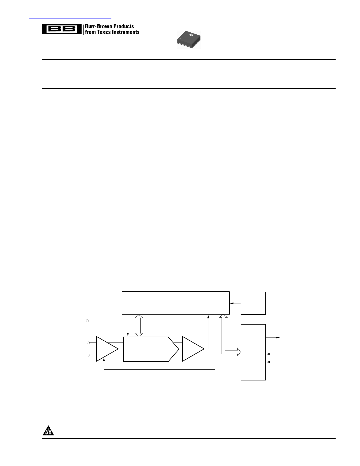
SAR
Control
D
OUT
Comparator
S/H Amp
CS/SHDN
DCLOCK
+In
V
REF
–In
CDAC
Serial
Interface
查询ADS7826IDRBR供应商
10/8/12-BIT HIGH SPEED 2.7 V microPOWER™ SAMPLING
ANALOG-TO-DIGITAL CONVERTER
FEATURES DESCRIPTION
• High Throughput at Low Supply Voltage
(2.7 V VCC)
– ADS7829: 12-bit 125 KSPS
– ADS7826: 10-bit 200 KSPS
– ADS7827: 8-bit 250 KSPS
• Very Wide Operating Supply VoltageL:
2.7 V to 5.25 V (as Low as 2.0 V With Reduced
Performance)
• Rail-to-Rail, Pseudo Differential Input
• Wide Reference Voltage: 50 mV to V
CC
• Micropower Auto Power-Down:
– Less Than 60 µW at 75 kHz, 2.7 V V
CC
• Low Power Down Current: 3 µA Max
• Ultra Small Chip Scale Package:
8-pin 3 x 3 PDSO (SON, Same Size as QFN)
• SPI™ Compatible Serial Interface
APPLICATIONS
• Battery Operated Systems
• Remote Data Acquisition
• Isolated Data Acquisition
• Simultaneous Sampling, Multichannel
Systems
The ADS7826/27/29 is a family of 10/8/12-bit sampling
analog-to-digital converters (A/D) with assured specifications at 2.7-V supply voltage. It requires very little
power even when operating at the full sample rate. At
lower conversion rates, the high speed of the device
enables it to spend most of its time in the power down
mode— the power dissipation is less than 60 µW at 7.5
kHz.
The ADS7826/27/29 also features operation from 2.0 V
to 5 V, a synchronous serial interface, and a differential
input. The reference voltage can be set to any level
within the range of 50 mV to VCC.
Ultra-low power and small package size make the
ADS7826/27/29 family ideal for battery operated systems. It is also a perfect fit for remote data acquisition
modules, simultaneous multichannel systems, and isolated data acquisition. The ADS7826/27/29 family is
available in a 3 x 3 8-pin PDSO (SON, same size as
QFN) package.
ADS7826
ADS7827
ADS7829
SLAS388–JUNE 2003
microPOWER is a trademark of Texas Instruments.
Please be aware that an important notice concerning availability, standard warranty, and use in critical applications of Texas Instruments
semiconductor products and disclaimers thereto appears at the end of this data sheet.
PRODUCTION DATA information is current as of publication date.
Products conform tospecifications per the terms ofTexas Instruments
standard warranty. Production processing does not necessarily includetestingof allparameters.
Copyright © 2003, Texas Instruments Incorporated
Page 2
www.ti.com
ADS7826
ADS7827
ADS7829
SLAS388–JUNE 2003
These devices have limited built-in ESD protection. The leads should be shorted together or the device placed in conductive foam
during storage or handling to prevent electrostatic damage to the MOS gates.
PACKAGE/ORDERING INFORMATION
MAXIMUM LINERARITY ERROR
PRODUCT INTEGRAL DIFFERENTIAL PACKAGE
ADS7829I ±2 ±2 SON-8 -40°C to 85°C F29 ADS7829IDRBR Tape and reel
ADS7829IB ±1.25 -1/1.25 SON-8 -40°C to 85° F29 ADS7829IBDRBR Tape and reel
ADS7826I ±1 ±1 SON-8 -40°C to 85°C F26 ADS7826IDRBR Tape and reel
ADS7827I ±1 ±1 SON-8 -40°C to 85°C F27 ADS7827IDRBR Tape and reel
ADS7829I ±2 ±2 SON-8 -40°C to 85°C F29 ADS7829IDRBT Tape and reel
ADS7829IB ±1.25 -1/1.25 SON-8 -40°C to 85°C F29 ADS7829IBDRBT Tape and reel
ADS7826I ±1 ±1 SON-8 -40°C to 85°C F26 ADS7826IDRBT Tape and reel
ADS7827I ±1 ±1 SON-8 -40°C to 85°C F27 ADS7827IDRBT Tape and reel
(1)
For detail drawing and dimension table, see end of this data sheet or package drawing file on web.
(2)
Performance Grade information is marked on the reel.
(LSB)
SPECIFICATION
TEMPERATURE PACKAGE ORDERING TRANSPORT
(1)
RANGE MARKING
(2)
NUMBER MEDIA
ABSOLUTE MAXIMUM RATINGS
over operating free-air temperature range (unless otherwise noted)
V
CC
Analog input -0.3 V to (VCC+ 0.3 V)
Logic input -0.3 V to 6 V
Case temperature 100°C
Junction temperature 150°C
Storage temperature 125°C
External reference voltage 5.5 V
(1)
Stresses beyond those listed under "absolute maximum ratings" may cause permanent damage to the device. These are stress ratings
only, and functional operation of the device at these or any other conditions beyond those indicated under "recommended operating
conditions" is not implied. Exposure to absolute-maximum-rated conditions for extended periods may affect device reliability.
(1)
6 V
2
Page 3
www.ti.com
www.ti.com
SPECIFICATIONS
At -40°C to 85°C, VCC= 2.7 V, V
= 2.5 V, unless otherwise specified.
ref
ADS7826
ADS7827
ADS7829
SLAS388–JUNE 2003
PARAMETER UNIT
ANALOG INPUT
Full-scale input +In - (-In) 0 V
span
Absolute input +In -0.2 VCC+0.2 -0.2 VCC+0.2 -0.2 VCC+0.2 -0.2 VCC+0.2 V
range
Capacitance 25 25 25 25 pF
Leakage current ±1 ±1 ±1 ±1 µA
SYSTEM PERFORMANCE
Resolution 12 12 10 8 Bits
No missing codes 12 11 10 8 Bits
Integral linearity error -1.25 ±0.4 1.25 -2 ±0.8 2 -1 ±0.3 1 -1 ±0.2 1 LSB
Differential linearity error -1 ±0.4 1.25 -2 ±0.8 2 -1 ±0.3 1 -1 ±0.2 1 LSB
Offset error -3 ±0.3 3 -3 ±0.6 3 -2 ±0.4 2 -1 ±0.4 1 LSB
Gain error -2 ±0.3 2 -2 ±0.6 2 -1 ±0.3 1 -1 ±0.2 1 LSB
Noise 33 33 33 33 µVrms
Power supply rejection 82 82 94 98 dB
SAMPLING DYNAMICS
Conversion time 12 12 10 8 DCLOCK
Acquisition time 1.5 1.5 1.5 1.5 DCLOCK
f
DCLOCK
Throughput 2.7 V ≤ V
(sample rate) ≤ 5.25 V
fsample
DYNAMIC CHARACTERISTICS
Total harmonic distortion -82 -80 -78 -72 dB
SINAD VIN= 2.5 Vpp at 72 70 62 50 dB
Spurious free VIN= 2.5 Vpp at 85 82 81 68 dB
dynamic range 1 kHz
(SFDR)
REFERENCE INPUT
Voltage range 2.7 V ≤VCC≤3.6 V 0.05 VCC-0.2 0.05 VCC-0.2 0.05 VCC-0.2 0.05 VCC-0.2 V
Resistance CS = GND, 5 5 5 5 GΩ
Current drain Full speed at V
DIGITAL INPUT/OUTPUT
Logic family CMOS CMOS CMOS CMOS
Logic levels
V
IH
V
IL
TEST
CONDITIONS
-IN -0.2 1.0 -0.2 1.0 -0.2 1.0 -0.2 1.0 V
CC
(2)
2.0 V ≤ V
CC
(3) (2)
< 2.7 V
1 kHz
f
= 0 Hz
SAMPLE
CS = V
CC
/2 12 60 12 60 20 100 24 120 µA
ref
f
= 7.5 kHz 0.8 0.8 0.8 0.8 µA
SAMPLE
CS = V
CC
IIH= +5 µA 2.0 5.5 2.0 5.5 2.0 5.5 2.0 5.5 V
IIL= +5 µA -0.3 0.8 -0.3 0.8 -0.3 0.8 -0.3 0.8 V
ADS7829IB ADS7829 ADS7826I ADS7827I
MIN TYP MAX MIN TYP MAX MIN TYP MAX MIN TYP MAX
0 V
ref
16 x fsample 16 x fsample 14 x fsample 12 x fsample kHz
125 125 200 250 kHz
75 75 85 100 kHz
5 5 5 5 GΩ
0.001 3 0.001 3 0.001 3 0.001 3 µA
ref
0 V
ref
0 V
ref
V
(1)
Cycles
Cycles
(1)
LSB means Least Significant Bit and is equal to V
/ 2Nwhere N is the resolution of ADC. For example, with V
ref
equal to 2.5 V, one
ref
LSB is 0.61 mV for a 12 bit ADC (ADS7829).
(2)
See the Typical Performance Curves for VCC= 5 V and V
(3)
The maximum clock rate of the ADS7826/27/29 are less than 1.2 MHz at 2 V ≤VCC<2.7 V. The recommended regerence voltage is
ref
= 5 V.
between 1.25 V to 1.024 V.
3
Page 4
www.ti.com
ADS7826
ADS7827
ADS7829
SLAS388–JUNE 2003
SPECIFICATIONS (continued)
At -40°C to 85°C, VCC= 2.7 V, V
PARAMETER UNIT
V
OH
V
OL
Data format Straight binary Straight binary Straight binary Straight binary
POWER SUPPLY REQUIREMENTS
VCC Operating range 2.7 3.6 2.7 3.6 2.7 3.6 2.7 3.6 V
Quiescent cur- Full speed
rent
Power down CS = V
TEMPERATURE RANGE
Specified performance -40 85 -40 85 -40 85 -40 85 °C
TEST
CONDITIONS
IOH= -250 µA 2.2 2.1 2.1 2.1 V
IOL= 250 µA 0.4 0.4 0.4 0.4 V
(3)
See
f
SAMPLE
f
SAMPLE
(2)
and
(2)
See
(4)
= 7.5 kHz 20 20 20 20 µA
(5)
,
= 7.5 kHz 180 180 180 180 µA
(6)
CC
= 2.5 V, unless otherwise specified.
ref
ADS7829IB ADS7829 ADS7826I ADS7827I
MIN TYP MAX MIN TYP MAX MIN TYP MAX MIN TYP MAX
2.0 2.7 2.0 2.7 2.0 2.7 2.0 2.7 V
3.6 5.25 3.6 5.25 3.6 5.25 3.6 5.25 V
220 350 220 350 250 350 260 350 µA
3 3 3 3 µA
(4)
Full speed: 125 ksps for ADS7829, 200 ksps for ADS7826, and 250 ksps for ADS7827.
(5)
f
= 1.2 MHz, CS = VCCfor 145 clock cycles out of every 160 for the ADS7829I and ADS7829IB.
DCLOCK
(6)
See the Power Dissipation section for more information regarding lower sample rates.
At -40°C to 85°C, VCC= 5 V, V
PARAMETER TEST CONDITIONS UNIT
SYSTEM PERFORMANCE
Resolution 12 12 10 8 Bits
No missing codes 12 11 10 8 Bits
Integral linearity error ±0.6 ±0.8 ±0.15 ±0.1 1 LSB
Differential linearity error ±0.5 ±0.8 ±0.15 ±0.1 1 LSB
ANALOG INPUT
Offset error ±2.6 ±2.6 ±1.2 ±0.7 LSB
Gain error ±1.2 ±1.2 ±0.2 ±0.1 LSB
REFERENCE INPUT
Voltage range 0.05 VCC0.05 VCC0.05 VCC0.05 V
(7)
LSB means Least Significant Bit . With V
= 5 V, unless otherwise specified.
ref
ADS7829IB ADS7829 ADS7826I ADS7827I
MIN TYP MAX MIN TYP MAX MIN TYP MAX MIN TYP MAX
equal to 5 V, one LSB is 1.22 mV for a 12 bit ADC.
ref
CC
(7)
V
4
Page 5
www.ti.com
www.ti.com
8
7
6
5
REF
+IN
−IN
GND
+V
DD
DCLOCK
DOUT
CS
/ SHDN
PDSO (SON−8) PACKAGE
(TOP VIEW)
1
2
3
4
ADS7826
ADS7827
ADS7829
SLAS388–JUNE 2003
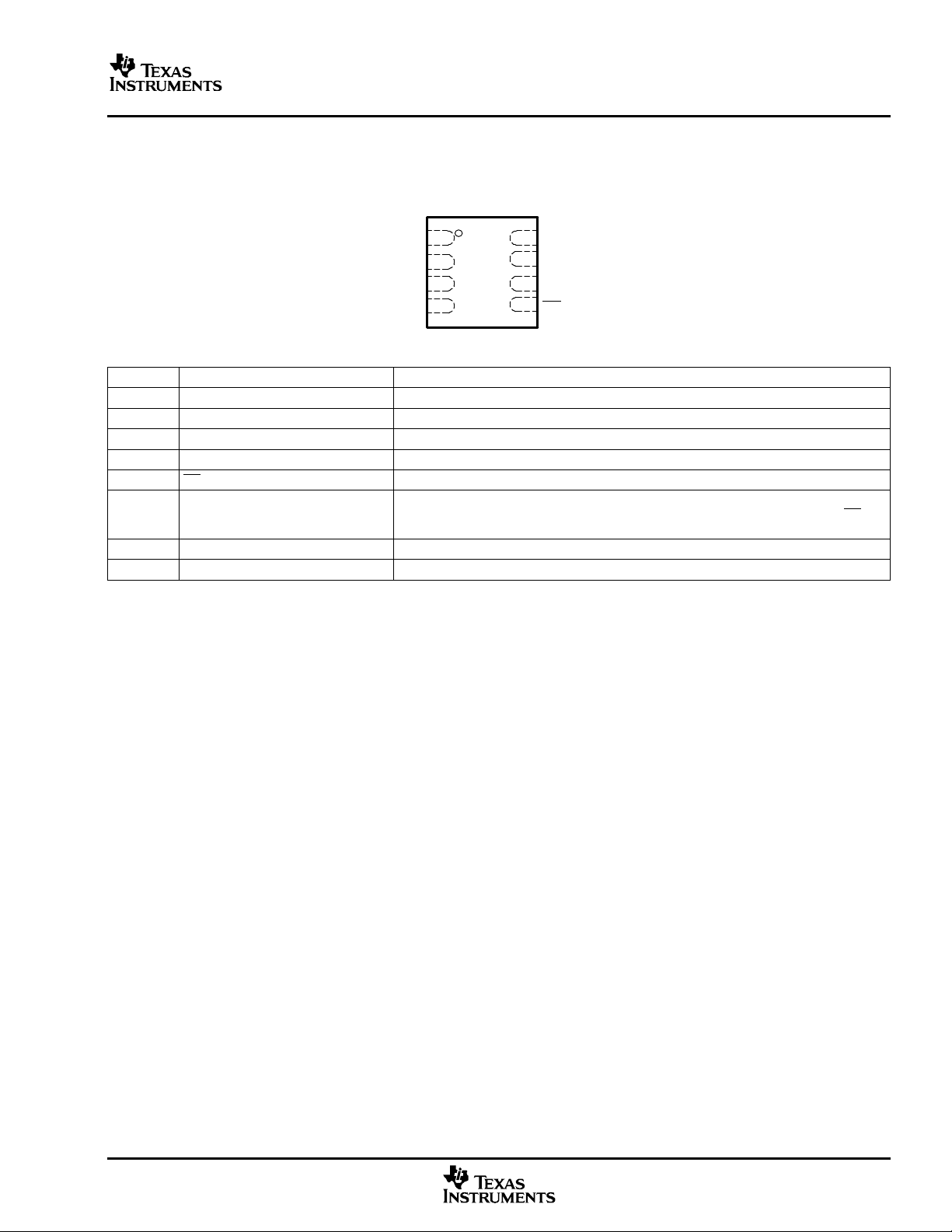
DEVICE INFORMATION
PIN DESCRIPTION
Terminal Functions
PIN NAME DESCRIPTION
1 V
2 +In Noninverting input
3 -In Inverting input. Connect to ground or to remote ground sense point.
4 GND Ground
5 CS/SHDN Chip select when LOW, shutdown mode when HIGH
6 DOUT The serial output data word is comprised of 12 bits of data. In operation the data is valid
7 DCLOCK Data Clock synchronizes the serial data transfer and determines conversion speed.
8 +V
ref
CC
Reference input
on the falling edge of DCLOCK. The second clock pulse after the falling edge of CS
enables the serial output. After one null bit, the data is valid for the next 12 edges.
Power supply
5
Page 6
www.ti.com
-1
-0.8
-0.6
-0.4
-0.2
0
0.2
0.4
0.6
0.8
1
0 512 1024 1536 2048 2560 3072 3584
Integral Linearity - LSB
Decimal Code
-1
-0.8
-0.6
-0.4
-0.2
0
0.2
0.4
0.6
0.8
1
0 128 256 384 512 640 768 896
Decimal Code
Integral Linearity - LSB
-0.5
-0.4
-0.3
-0.2
-0.1
0
0.1
0.2
0.3
0.4
0.5
0 32 64 96 128 160 192 224
Decimal Code
Integral Linearity - LSB
ADS7826
ADS7827
ADS7829
SLAS388–JUNE 2003
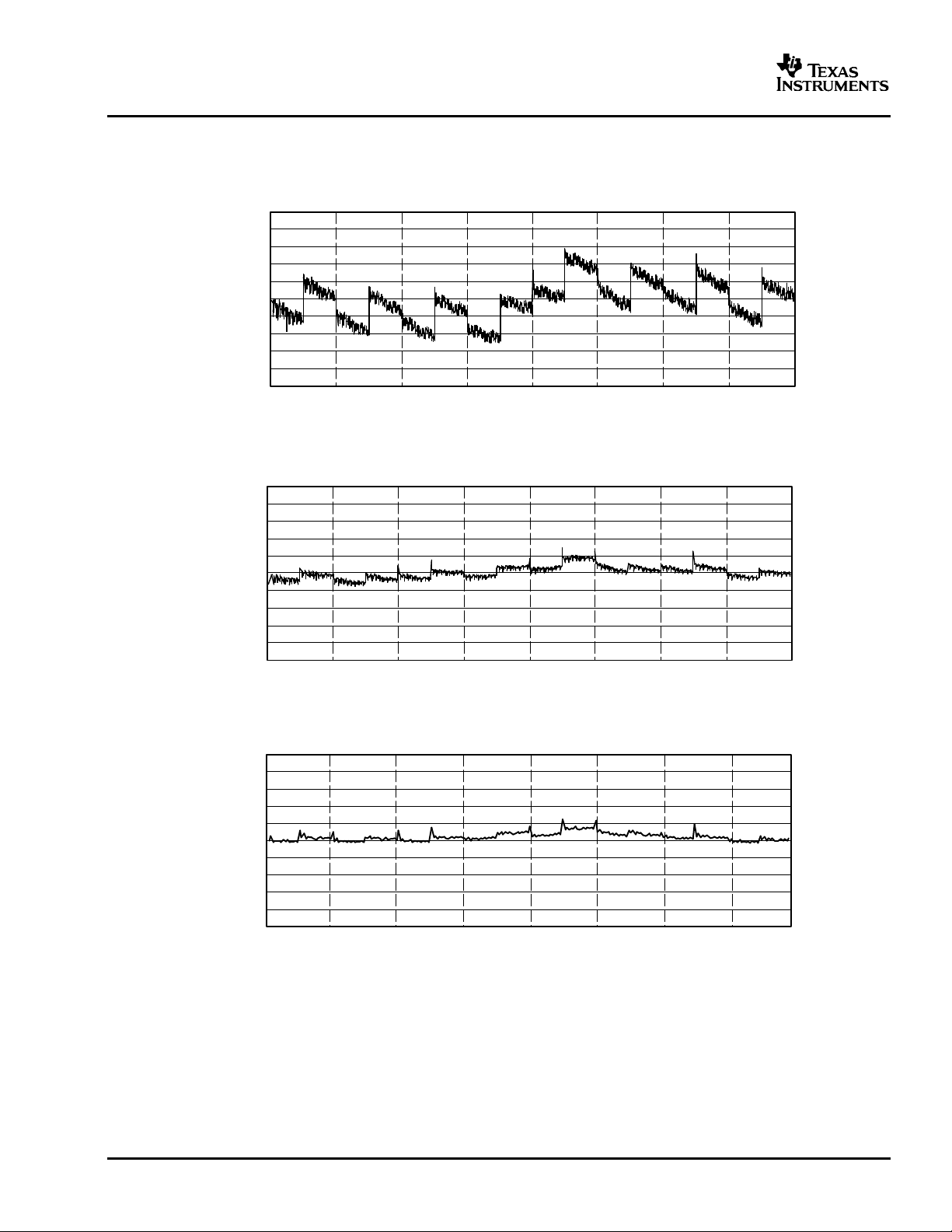
TYPICAL CHARACTERISTICS
At TA= 25°C, VCC= 2.7 V, V
ADS7829 INTEGRAL LINEARITY
ADS7826 INTEGRAL LINEARITY
= 25 V, (unless otherwise specified)
ref
Figure 1
ADS7827 INTEGRAL LINEARITY
6
Figure 2
Figure 3
Page 7

www.ti.com
www.ti.com
-1
-0.8
-0.6
-0.4
-0.2
0
0.2
0.4
0.6
0.8
1
0 512 1024 1536 2048 2560 3072 3584
Decimal Code
Differential Linearity - LSB
-1
-0.8
-0.6
-0.4
-0.2
0
0.2
0.4
0.6
0.8
1
0 128 256 384 512 640 768 896
Decimal Code
Differential Linearity - LSB
-0.5
-0.4
-0.3
-0.2
-0.1
0
0.1
0.2
0.3
0.4
0.5
0 32 64 96 128 160 192 224
Decimal Code
Differential Linearity - LSB
At TA= 25°C, VCC= 2.7 V, V
TYPICAL CHARACTERISTICS (continued)
= 25 V, (unless otherwise specified)
ref
ADS7829 DIFFERENTIAL LINEARITY
Figure 4
ADS7826 DIFFERENTIAL LINEARITY
ADS7826
ADS7827
ADS7829
SLAS388–JUNE 2003
ADS7827 DIFFERENTIAL LINEARITY
Figure 5
Figure 6
7
Page 8

www.ti.com
−0.2
−0.15
−0.1
−0.05
0
0.05
0.1
0.15
0.2
−40 −20 0 20 40 60 80
ADS7826
Delta From 25
TA − Free-Air Temperature − °C
C
°
− LSB
ADS7827
ADS7829
−0.2
−0.15
−0.1
−0.05
0
0.05
0.1
0.15
0.2
−40 −20 0 20 40 60 80
ADS7826
ADS7827
Delta From 25
TA − Free-Air Temperature − °C
C
°
− LSB
ADS7829
−0.4
−0.3
−0.2
−0.1
0
0.1
0.2
0.3
0.4
−40 −20 0 20 40 60 80
ADS7829
Delta From 25
TA − Free-Air Temperature − °C
C
°
− LSB
ADS7826
ADS7827
−0.4
−0.3
−0.2
−0.1
0
0.1
0.2
0.3
0.4
−40 −20
0
20 40 60 80
ADS7826
ADS7827
ADS7829
Delta From 25
TA − Free-Air Temperature − °C
C
°
− LSB
−0.1
0
0.1
0.2
0.3
0.4
0.5
−40 −20 0 20 40 60 80
ADS7826
ADS7827
ADS7829
Delta From 25
TA − Free-Air Temperature − °C
C
°
− LSB
−0.2
−0.1
0
0.1
0.2
0.3
0.4
−40 −20 0 20 40 60 80
ADS7827
Delta From 25
TA − Free-Air Temperature − °C
C
°
− LSB
ADS7829
ADS7826
ADS7826
ADS7827
ADS7829
SLAS388–JUNE 2003
At TA= 25°C, VCC= 2.7 V, V
TYPICAL CHARACTERISTICS (continued)
= 25 V, (unless otherwise specified)
ref
CHANGE IN MINIMUM INTEGRAL LINEARITY CHANGE IN MAXIMUM INTEGRAL LINEARITY
vs vs
FREE-AIR TEMPERATURE FREE-AIR TEMPERATURE
Figure 7.
Figure 8.
CHANGE IN MINIMUM DIFFERENTIAL LINEARITY CHANGE IN MAXIMUM DIFFERENTIAL LINEARITY
vs vs
FREE-AIR TEMPERATURE FREE-AIR TEMPERATURE
8
Figure 9.
Figure 10.
CHANGE IN OFFSET ERROR CHANGE IN GAIN ERROR
vs vs
FREE-AIR TEMPERATURE FREE-AIR TEMPERATURE
Figure 11.
Figure 12.
Page 9

www.ti.com
www.ti.com
−0.2
−0.1
0
0.1
0.2
0.3
0.4
0.5
2.7 3.2 3.7 4.2 4.7 5.2
ADS7826
ADS7827
ADS7829
V
ref
= 2.5 V
VCC − Supply Voltage − V
Delta From 2.7 V − LSB
−50
−40
−30
−20
−10
0
10
20
30
40
50
−40 −20 20 40 60 800
Quiescent Current − mA
I
O
−
TA − Free-Air Temperature − °C
−0.5
−0.4
−0.3
−0.2
−0.1
0
0.1
0.2
2.7 3.2 3.7 4.2 4.7 5.2
ADS7826
ADS7827
ADS7829
V
ref
= 2.5 V
VCC − Supply Voltage − V
Delta From 2.7 V − LSB
−0.3
−0.2
−0.1
0
0.1
0.2
0.3
2.7 3.2 3.7 4.2 4.7 5.2
ADS7826
ADS7827
ADS7829
V
ref
= 2.5 V
VCC − Supply Voltage − V
Delta From 2.7 V − LSB
−0.1
−0.08
−0.06
−0.04
−0.02
0
0.02
0.04
0.06
0.08
0.1
2.7 3.2 3.7 4.2 4.7 5.2
ADS7826
V
ref
= 2.5 V
VCC − Supply Voltage − V
Delta From 2.7 V − LSB
ADS7829
ADS7827
0
1
2
3
4
5
6
2.7 3.2 3.7 4.2 4.7 5.2
ADS7826
ADS7827
ADS7829
VCC − Supply Voltage − V
Delta From 2.7 V − LSB
V
ref
= 2.5 V
At TA= 25°C, VCC= 2.7 V, V
TYPICAL CHARACTERISTICS (continued)
= 25 V, (unless otherwise specified)
ref
ADS7826
ADS7827
ADS7829
SLAS388–JUNE 2003
CHANGE IN QUIESCENT CURRENT CHANGE IN MAXIMUM INTEGRAL LINEARITY
vs vs
FREE-AIR TEMPERATURE SUPPLY VOLTAGE
Figure 13.
Figure 14.
CHANGE IN MINIMUM INTEGRAL LINEARITY CHANGE IN MAXIMUM DIFFERENTIAL LINEARITY
vs vs
SUPPLY VOLTAGE SUPPLY VOLTAGE
Figure 15.
Figure 16.
CHANGE IN MINIMUM INTEGRAL LINEARITY CHANGE IN OFFSET ERROR
vs vs
SUPPLY VOLTAGE SUPPLY VOLTAGE
Figure 17.
Figure 18.
9
Page 10

www.ti.com
0
20
40
60
80
100
120
140
160
180
200
2.7 3.2 3.7 4.2 4.7 5.2
ADS7829
V
ref
= 2.5 V
ADS7827
VCC − Supply Voltage − V
Delta From 2.7 V − Aµ
ADS7826
0
0.2
0.4
0.6
0.8
1
1.2
2.7 3.2 3.7 4.2 4.7 5.2
ADS7826
ADS7827
ADS7829
VCC − Supply Voltage − V
Delta From 2.7 V − LSB
V
ref
= 2.5 V
Sample Rate − kHz
15
10
5
0 25 50 75 100 125 150
Reference Current −
20
30
175 200 225 250
25
0
Aµ
Reference Voltage - V
0.2
0
-0.4
1 2 3
Change in Offset - LSB
0.6
0.8
1.2
4 5
1
-0.2
-0.8
0.4
-0.6
VCC = 5 V
Reference Voltage - V
5
4
2
0.1 1
Peak-To-Peak Noise - LSB
6
8
10
10
9
3
1
7
VCC = 5 V
0
Reference Voltage - V
0.5
0
-1
0 2 3
Change in Gain - dB
1
1.5
2.5
4 5
2
-0.5
-1.5
VCC = 5 V
ADS7826
ADS7827
ADS7829
SLAS388–JUNE 2003
At TA= 25°C, VCC= 2.7 V, V
CHANGE IN GAIN CHANGE IN QUIESCENT CURRENT
SUPPLY VOLTAGE SUPPLY VOLTAGE
TYPICAL CHARACTERISTICS (continued)
= 25 V, (unless otherwise specified)
ref
vs vs
Figure 19.
Figure 20.
ADS7829
REFERENCE CURRENT CHANGE IN OFFSET ERROR
vs vs
SAMPLE RATE REFERENCE VOLTAGE
Figure 21.
Figure 22.
ADS7829 ADS7829
CHANGE IN GAIN ERROR PEAK-TO-PEAK NOISE
vs vs
REFERENCE VOLTAGE REFERENCE VOLTAGE
10
Figure 23.
Figure 24.
Page 11

www.ti.com
www.ti.com
Reference Voltage - V
11
10.75
10.25
0.1 1
Effective Number of Bits - rms
11.25
11.5
12
10
11.75
10.5
10
VCC = 5 V
Change in Integral
Linearity - LSB
Change in Differential
Linearity - LSB
VCC = 5 V
Reference Voltage - V
0.05
-0.05
1 2 3 4
Data From 2.5 V Reference - LSB
0.10
0.20
5
0.15
0
-0.10
0
10
20
30
40
50
60
70
80
90
100
1
10
100
1000
f − Frequency − kHz
Spurious Free Dynamic Range
Signal-To-Noise Ratio − dB
Spurious Free Dynamic Range
Signal-To-Noise
0
10
20
30
40
50
60
70
80
90
100
1 10 100 1000
f - frequency - kHz
Signal-To-Noise+Distortion - dB
0
10
20
30
40
50
60
70
80
90
100
1 10 100 1000
f − Frequency − kHz
Spurious Free Dynamic Range
Signal-To-Noise Ratio − dB
Spurious Free Dynamic Range
Signal-To-Noise
-100
-90
-80
-70
-60
-50
-40
-30
-20
-10
0
1 10 100 1000
f - Frequency - kHz
THD - Total Harmonic Distortion - dB
At TA= 25°C, VCC= 2.7 V, V
TYPICAL CHARACTERISTICS (continued)
= 25 V, (unless otherwise specified)
ref
ADS7826
ADS7827
ADS7829
SLAS388–JUNE 2003
CHANGE IN INTEGRAL and ADS7829
ADS7829
DIFFERENTIAL LINEARITY EFFECTIVE NUMBER OF BITS
vs vs
REFERENCE VOLTAGE REFERENCE VOLTAGE
Figure 25.
Figure 26.
ADS7829
SPURIOUS FREE DYNAMIC RANGE ADS7829
and SIGNAL-TO-NOISE RATIO SIGNAL-TO-NOISE + DISTORTION
vs vs
SAMPLE FREQUENCY FREQUENCY
Figure 27.
Figure 28.
ADS7826
ADS7829 SPURIOUS FREE DYNAMIC RANGE
TOTAL HARMONIC DISTORTION and SIGNAL-TO-NOISE RATIO
vs vs
FREQUENCY FREQUENCY
Figure 29.
Figure 30.
11
Page 12

www.ti.com
-100
-90
-80
-70
-60
-50
-40
-30
-20
-10
0
1 10 100 1000
f - Frequency - kHz
THD - Total Harmonic Distortion - dB
0
10
20
30
40
50
60
70
80
90
100
1 10 100 1000
f - frequency - kHz
Signal-To-Noise+Distortion - dB
0
20
40
60
80
100
1 10 100 1000
f − Frequency − kHz
Spurious Free Dynamic Range
Signal-To-Noise Ratio − dB
Spurious Free Dynamic Range
Signal-To-Noise
0
20
40
60
80
100
1
10 100 1000
f - frequency - kHz
Signal-To-Noise+Distortion - dB
-100
-90
-80
-70
-60
-50
-40
-30
-20
-10
0
1 10 100 1000
f - Frequency - kHz
THD - Total Harmonic Distortion - dB
ADS7826
ADS7827
ADS7829
SLAS388–JUNE 2003
At TA= 25°C, VCC= 2.7 V, V
TYPICAL CHARACTERISTICS (continued)
= 25 V, (unless otherwise specified)
ref
SIGNAL-TO-NOISE + DISTORTION TOTAL HARMONIC DISTORTION
ADS7826 ADS7826
vs vs
FREQUENCY FREQUENCY
Figure 31.
Figure 32.
ADS7827
SPURIOUS FREE DYNAMIC RANGE ADS7827
and SIGNAL-TO-NOISE RATIO SIGNAL-TO-NOISE + DISTORTION
vs vs
FREQUENCY FREQUENCY
12
Figure 33.
Figure 34.
ADS7827
TOTAL HARMONIC DISTORTION
vs
FREQUENCY
Figure 35.
Page 13

www.ti.com
www.ti.com
ADS7826
ADS7827
ADS7829
SLAS388–JUNE 2003
THEORY OF OPERATION
The ADS7826/27/29 is a family of micropower classic The input current on the analog inputs depends on a
successive approximation register (SAR) number of factors: sample rate, input voltage, source
analog-to-digital (A/D) converters. The architecture is impedance, and power down mode. Essentially, the
based on capacitive redistribution which inherently current into the ADS7826/27/29 family charges the
includes a sample/hold function. The converter is internal capacitor array during the sample period.
fabricated on a 0.6 µm CMOS process. The After this capacitance has been fully charged, there is
architecture and process allow the ADS7826/27/29 no further input current. The source of the analog
family to acquire and convert an analog signal at up input voltage must be able to charge the input
to 200K/250K/125K conversions per second capacitance (25 pF) to a 10/8/12-bit settling level
respectively while consuming very little power. within 1.5 DCLOCK cycles. When the converter goes
The ADS7826/27/29 family requires an external
reference, an external clock, and a single power
source (VCC). The external reference can be any Care must be taken regarding the absolute analog
voltage between 50 mV and VCC. The value of the input voltage. To maintain the linearity of the
reference voltage directly sets the range of the converter, the -In input should not drop below GND analog input. The reference input current depends on 200 mV or exceed GND + 1 V. The +In input should
the conversion rate of the ADS7826/27/29 family. always remain within the range of GND - 200 mV to
The minimum external clock input to DCLOCK can be
as low as 10 kHz. The maximum external clock
frequency is 2 MHz for ADS7829, 2.8 MHz for
ADS7826 and 3 MHz for ADS7827 respectively. The
duty cycle of the clock is essentially unimportant as
long as the minimum high and low times are at least
400 ns (VCC= 2.7 V or greater). The minimum
DCLOCK frequency is set by the leakage on the
capacitors internal to the ADS7826/27/29 family.
The analog input is provided to two input pins: +In
and -In. When a conversion is initiated, the differential
input on these pins is sampled on the internal
capacitor array. While a conversion is in progress,
both inputs are disconnected from any internal
function.
The digital result of the conversion is clocked out by
the DCLOCK input and is provided serially, most
significant bit first, on the D
that is provided on the D
OUT
pin. The digital data
OUT
pin is for the conversion
currently in progress—there is no pipeline delay.
ANALOG INPUT output code. When the external reference is 50 mV,
The +In and -In input pins allow for a differential input
signal. Unlike some converters of this type, the -In
input is not re-sampled later in the conversion cycle.
When the converter goes into the hold mode, the
voltage difference between +In and -In is captured on For more information regarding noise, consult the
the internal capacitor array. typical performance curves Effective Number of Bits
The range of the -In input is limited to -0.2 V to 1 V.
Because of this, the differential input can be used to
reject only small signals that are common to both
inputs. Thus, the -In input is best used to sense a
remote signal ground that may move slightly with
respect to the local ground potential.
into the hold mode or while it is in the power down
mode, the input impedance is greater than 1 GΩ.
VCC+ 200 mV. Outside of these ranges, the
converter’s linearity may not meet specifications.
REFERENCE INPUT
The external reference sets the analog input range.
The ADS7826/27/29 family operates with a reference
in the range of 50 mV to VCC. There are several
important implications of this.
As the reference voltage is reduced, the analog
voltage weight of each digital output code is reduced.
This is often referred to as the LSB (least significant
bit) size and is equal to the reference voltage divided
by 2N(where N is 12 for ADS7829, 10 for ADS7826,
and 8 for ADS7827). This means that any offset or
gain error inherent in the A/D converter appears to
increase, in terms of LSB size, as the reference
voltage is reduced.
The noise inherent in the converter also appears to
increase with lower LSB size. With a 2.5 V reference,
the internal noise of the converter typically contributes
only 0.32 LSB peak-to-peak of potential error to the
the potential error contribution from the internal noise
is 50 times larger —16 LSBs. The errors due to the
internal noise are gaussian in nature and can be
reduced by averaging consecutive conversion results.
vs Reference Voltage and Peak-to-Peak Noise vs
Reference Voltage (only curves for ADS7829 are
shown). Note that the effective number of bits
(ENOB) figure is calculated based on the converter’s
signal-to-(noise + distortion) ratio with a 1 kHz, 0 dB
input signal. SINAD is related to ENOB as follows:
13
Page 14

www.ti.com
t
CYC
Power
Down
t
SU(CS)
t
CSD
Hi-Z
Null
Bit
B11
(MSB)
B10 B9 B8 B7 B6 B5 B4 B3 B2 B1 B0
1
Null
Bit
B11 B10 B9 B8
Hi-Z
t
SMPL
t
CONV
t
DATA
CS
/SHDN
DCLOCK
D
OUT
t
CYC
Power
Down
t
SU(CS)
t
CSD
Hi-Z
Null
Bit
B9
(MSB)
B8 B4 B3 B2 B1 B0
1
Null
Bit
MSB
Hi-Z
CS
/SHDN
DCLOCK
D
OUT
Hi-Z
Null
Bit
B7
(MSB)
B6 B4 B3 B2 B1 B0
1
Null
Bit
MSB
Hi-Z
t
SMPL
t
CONV
ADS7826
D
OUT
ADS7827
ADS7826
ADS7827
ADS7829
SLAS388–JUNE 2003
SINAD = 6.02 × ENOB + 1.76
With lower reference voltages, extra care should be
taken to provide a clean layout including adequate
bypassing, a clean power supply, a low-noise
reference, and a low-noise input signal. Because the
LSB size is lower, the converter is more sensitive to
external sources of error such as nearby digital
signals and electromagnetic interference.
Serial Interface
The ADS7826/27/29 family communicates with
microprocessors and other digital systems via a
synchronous 3-wire serial interface. Timings for
ADS7829 are shown in Figure 36 and Table 1. The
DCLOCK signal synchronizes the data transfer with
each bit being transmitted on the falling edge of
DCLOCK. Most receiving systems capture the
bitstream on the rising edge of DCLOCK. However, if
DIGITAL INTERFACE the minimum hold time for D
Signal Levels
The digital inputs of the ADS7826/27/29 family can
accommodate logic levels up to 6 V regardless of the
value of VCC. Thus, the ADS7826/27/29 family can be
powered at 3 V and still accept inputs from logic
powered at 5 V.
The CMOS digital output (D
) swings 0 V to VCC. If
OUT
VCCis 3 V and this output is connected to a 5-V
CMOS logic input, then that IC may require more
supply current than normal and may have a slightly
longer propagation delay.
system can use the falling edge of DCLOCK to
capture each bit.
The timings for ADS7826 and ADS7827 serial
interface are shown in Figure 37 and Table 1. The
DCLOCK signal synchronizes the data transfer with
each bit being transmitted on the falling edge of
DCLOCK. Most receiving systems capture the
bitstream on the rising edge of DCLOCK. However, if
the minimum hold time for D
system can use the fallng edge of DCLOCK to
capture each bit.
is acceptable, the
OUT
is acceptable, athe
OUT
14
After completing the data transfer, if further clocks are applied with CS LOW, the A/D outputs LSB-First data then
followed with zeroes indefinitely.
Figure 36. ADS7829 Timing
Figure 37. ADS7826 and ADS7827 Timing
Page 15

www.ti.com
www.ti.com
ADS7826
ADS7827
ADS7829
SLAS388–JUNE 2003
Table 1. Timing Specifications (VCC= 2.7 V and Above -40°C to 85°C
SYMBOL DESCRIPTION MIN TYP MAX UNIT
t
SAMPLE
t
CONV
t
CYC
t
CSD
t
SU(CS)
t
h(DO)
t
d(DO)
t
dis
t
en
t
f
t
r
Analog input sample time 1.5 2.0 DCLOCK
Conversion time ADS7829I or ADS7829IB 12 DCLOCK
ADS7826I 11
ADS7827I 9
Cycle time ADS7829I or ADS7829IB 16 DCLOCK
ADS7826 14
ADS7827 12
CS falling to DCLOCK LOW 0 ns
CS falling to DCLOCK rising 30 ns
DCLOCK falling to current D
DCLOCK falling to next D
CS rising to D
DCLOCK falling to D
D
fall time 90 200 ns
OUT
D
rise time 110 220 ns
OUT
3-state 40 80 ns
OUT
OUT
not valid 15 ns
OUT
valid 130 200 ns
OUT
enabled 75 175 ns
Cycles
Cycles
Cycles
A falling CS signal initiates the conversion and data
transfer. The first 1.5 to 2.0 clock periods of the
conversion cycle are used to sample the input signal.
After the second falling DCLOCK edge, D
OUT
enabled and outputs a LOW value for one clock
period. For the next N (N is 12 for ADS7829, 10 for
ADS7826, and 8 for ADS7827) DCLOCK periods,
D
outputs the conversion result, most significant
OUT
bit first. After the least significant bit has been sent,
D
goes to 3-state after the rising edge of CS. A
OUT
new conversion is initiated only when CS has been
taken high and returned low again.
Table 2. Ideal Input Voltages and Output Codes (ADS7829 Shown as an Example)
DESCRIPTION ANALOG VALUE DIGITAL OUTPUT
FULL SCALE RANGE V
LEAST SIGNIFICANT BIT (LSB) V
Full scale V
Midscale V
Midscale - 1 LSB V
Zero 0 V 0000 0000 0000 000
ref
/4096 BINARY CODE HEX CODE
ref
- 1 LSB 1111 1111 1111 FFF
ref
/2 1000 0000 0000 800
ref
/2 - 1 LSB 0111 1111 1111 7FF
ref
DATA FORMAT
is
The output data from the ADS7826/27/29 family is in
straight binary format. ADS7829 out is shown in
Table 2, as an example. This table represents the
ideal output code for the given input voltage and does
not include the effects of offset, gain error, or noise.
For ADS7826 the last two LSB’s are don’t cares,
while for ADS7827 the last four LSB’s are don’t
cares.
STRAIGHT BINARY
15
Page 16

www.ti.com
D
OUT
1.4 V
Test Point
3 k
100 pF
C
LOAD
t
r
D
OUT
t
f
Test Point
3 k
CS/SHDN
D
OUT
D
OUT
90%
10%
1
B11
2
CS/SHDN
DCLOCK
D
OUT
DCLOCK
V
IL
100 pF
Voltage Waveforms for t
en
D
OUT
t
h(DO)
Voltage Waveforms for D
OUT
Delay Times, t
dDO
V
OH
V
OL
V
OH
V
OL
D
OUT
t
h(DO)
C
LOAD
V
CC
t
dis
Waveform 2, t
en
t
dis
Waveform 1
Load Circuit for t
dis
and t
en
t
dis
V
IH
Voltage Waveforms for t
dis
Waveform 1
(1)
Waveform 2
(2)
t
en
V
OL
Load Circuit for t
dDO
, tr, and t
f
Voltage W aveforms for D
OUT
Rise and Fall Times, tr, t
f
ADS7826
ADS7827
ADS7829
SLAS388–JUNE 2003
(1)
Waveform 1 is for an output with internal conditions such that the output is HIGH unless disabled by the output control.
(2)
Waveform 2 is for an output with internal conditions such that the output is LOW unless disabled by the output control.
Figure 38. Timing Diagrams and Test Circuits for the Parameters in Table 1.
POWER DISSIPATION
The architecture of the converter, the semiconductor This way, the converter spends the longest possible
fabrication process, and a careful design allows the time in the power down mode. This is very important
ADS7826/27/29 family to convert at the full sample as the converter not only uses power on each
rate while requiring very little power. But, for the DCLOCK transition (as is typical for digital CMOS
absolute lowest power dissipation, there are several components) but also uses some current for the
things to keep in mind. analog circuitry, such as the comparator. The analog
The power dissipation of the ADS7826/27/29 family
scales directly with conversion rate. Therefore, the
first step to achieving the lowest power dissipation is The current consumption of the ADS7826/27/29
to find the lowest conversion rate that satisfies the family versus sample rate. For this graph, the
section dissipates power continuously, until the
power-down mode is entered.
requirements of the system. converter is clocked at maximum DCLOCK rate
In addition, the ADS7826/27/29 family is in power
down mode under two conditions: when the
conversion is complete and whenever CS is HIGH.
Ideally, each conversion occurs as quickly as
possible, preferably, at DCLOCK rate.
16
regardless of the sample rate —CS is HIGH for the
remaining sample period. Figure 4 also shows current
consumption versus sample rate. However, in this
case, the minimum DCLOCK cylce time is used—CS
is HIGH for one DCLOCK cycle.
Page 17

www.ti.com
www.ti.com
ADS7826
ADS7827
ADS7829
SLAS388–JUNE 2003
There is an important distinction between the power The reference should be similarly bypassed with a
down mode that is entered after a conversion is 0.1-µF capacitor. Again, a series resistor and large
complete and the full power-down mode which is capacitor can be used to lowpass filter the reference
enabled when CS is HIGH. While both shutdown the voltage. If the reference voltage originates from an
analog section, the digital section is completely op-amp, be careful that the op-amp can drive the
shutdown only when CS is HIGH. Thus, if CS is left bypass capacitor without oscillation (the series
LOW at the end of a conversion and the converter is resistor can help in this case). Keep in mind that
continually clocked, the power consumption is not as while the ADS7826/27/29 family draws very little
low as when CS is HIGH. current from the reference on average, there are still
Power dissipation can also be reduced by lowering
the power supply voltage and the reference voltage.
The ADS7826/27/29 family operates over a V
CC
range of 2.0 V to 5.25 V. However, at voltages below offers no inherent rejection of noise or voltage
2.7 V, the converter does not run at the maximum variation in regards to the reference input. This is of
sample rate. See the typical performance curves for particular concern when the reference input is tied to
more information regarding power supply voltage and the power supply. Any noise and ripple from the
maximum sample rate. supply appears directly in the digital results. While
LAYOUT
For optimum performance, care should be taken with
the physical layout of the ADS7826/27/29 family
circuitry. This is particularly true if the reference
voltage is low and/or the conversion rate is high. At a
125-kHz to 250-kHz conversion rate, the
ADS7826/27/29 family makes a bit decision every
800 ns to 400 ns. That is, for each subsequent bit
decision, the digital output must be updated with the
results of the last bit decision, the capacitor array
appropriately switched and charged, and the input to
the comparator settled, for example the ADS7829, to
a 12-bit level all within one clock cycle.
The basic SAR architecture is sensitive to spikes on
the power supply, reference, and ground connections Figure 39 and Figure 40 show some typical
that occur just prior to latching the comparator output. application circuits the ADS7826/27/29 family. Figure
Thus, during any single conversion for an n-bit SAR 39 uses an ADS7826/27/29 and a multiplexer to
converter, there are n windows in which large provide for a flexible data acquisition circuit. A
external transient voltages can easily affect the resistor string provides for various voltages at the
conversion result. Such spikes might originate from multiplexer input. The selected voltage is buffered
switching power supplies, digital logic, and high and driven into V
power devices, to name a few. This particular source range of the ADS7826/27/29 family programmable to
of error can be very difficult to track down if the glitch 100 mV, 200 mV, 300 mV, or 400 mV. The 100-mV
is almost synchronous to the converter’s DCLOCK range would be useful for sensors such as
signal—as the phase difference between the two thermocouple shown.
changes with time and temperature, causing sporadic
misoperation.
With this in mind, power to the ADS7826/27/29 family the reference input is connected directly to the power
should be clean and well bypassed. A 0.1-µF ceramic supply. The 5-Ω resistor and 1-µF to 10-µF capacitor
bypass capacitor should be placed as close to the filters the microcontroller noise on the supply, as well
ADS7826/27/29 family package as possible. In as any high-frequency noise from the supply itself.
addition, a 1-µ to 10-µF capacitor and a 5-Ω or 10-Ω The exact values should be picked such that the filter
series resistor may be used to lowpass filter a noisy provides adequate rejection of the noise.
supply.
instantaneous current demands placed on the
external reference circuitry.
Also, keep in mind that the ADS7826/27/29 family
high frequency noise can be filtered out as described
in the previous paragraph, voltage variation due to
the line frequency (50 Hz or 60 Hz), can be difficult to
remove.
The GND pin on the ADS7826/27/29 family must be
placed on a clean ground point. In many cases, this
is the analog ground. Avoid connecting the GND pin
too close to the grounding point for a microprocessor,
microcontroller, or digital signal processor. If needed,
run a ground trace directly from the converter to the
power supply connection point. The ideal layout
includes an analog ground plane for the converter
and associated analog circuitry.
APPLICATION CIRCUITS
. As shown in Figure 39, the input
ref
Figure 39 shows a basic data acquisition system. The
ADS7826/27/29 family input range is 0 V to VCC, as
17
Page 18

www.ti.com
ADS7826/27/29
µP
DCLOCK
D
OUT
CS/SHDN
A
0
A
1
U
3
U
4
U
1
U
2
Thermocouple
ISO Thermal Block
MUX
OPA237
0.3 V
0.4 V
0.2 V
0.1 V
+3 V
R
2
59 kΩ
R
4
1 kΩ
R
3
500 kΩ
R
5
500 Ω
R
7
5 Ω
C
3
0.1 µ
F
C
4
10 µ F
C
5
0.1 µ
F
R
6
1 MΩ
R
1
1
TC
2
TC
1
TC
3
+3 V
C
2
0.1 µ F
C
1
10 µ
F
+3 V
R
8
26 kΩ
R
9
1 kΩ
R
10
1 kΩ
R
11
1 kΩ
R
12
1 kΩ
V
REF
ADS7826/27/29
V
CC
CS
D
OUT
DCLOCK
V
REF
+In
–In
GND
+
+
5
Microcontroller
+2.7V to +3.6V
1 F to
10 F
1 F to
10 F
0.1 F
ADS7826
ADS7827
ADS7829
SLAS388–JUNE 2003
Figure 39. Thermocouple Application Using a MUX to Scale the Input Range of the ADS7826/27/29 family
18
Figure 40. Basic Data Acquisition System
Page 19

Page 20

IMPORTANT NOTICE
Texas Instruments Incorporated and its subsidiaries (TI) reserve the right to make corrections, modifications,
enhancements, improvements, and other changes to its products and services at any time and to discontinue
any product or service without notice. Customers should obtain the latest relevant information before placing
orders and should verify that such information is current and complete. All products are sold subject to TI’s terms
and conditions of sale supplied at the time of order acknowledgment.
TI warrants performance of its hardware products to the specifications applicable at the time of sale in
accordance with TI’s standard warranty. Testing and other quality control techniques are used to the extent TI
deems necessary to support this warranty . Except where mandated by government requirements, testing of all
parameters of each product is not necessarily performed.
TI assumes no liability for applications assistance or customer product design. Customers are responsible for
their products and applications using TI components. To minimize the risks associated with customer products
and applications, customers should provide adequate design and operating safeguards.
TI does not warrant or represent that any license, either express or implied, is granted under any TI patent right,
copyright, mask work right, or other TI intellectual property right relating to any combination, machine, or process
in which TI products or services are used. Information published by TI regarding third-party products or services
does not constitute a license from TI to use such products or services or a warranty or endorsement thereof.
Use of such information may require a license from a third party under the patents or other intellectual property
of the third party, or a license from TI under the patents or other intellectual property of TI.
Reproduction of information in TI data books or data sheets is permissible only if reproduction is without
alteration and is accompanied by all associated warranties, conditions, limitations, and notices. Reproduction
of this information with alteration is an unfair and deceptive business practice. TI is not responsible or liable for
such altered documentation.
Resale of TI products or services with statements different from or beyond the parameters stated by TI for that
product or service voids all express and any implied warranties for the associated TI product or service and
is an unfair and deceptive business practice. TI is not responsible or liable for any such statements.
Following are URLs where you can obtain information on other Texas Instruments products and application
solutions:
Products Applications
Amplifiers amplifier.ti.com Audio www.ti.com/audio
Data Converters dataconverter.ti.com Automotive www.ti.com/automotive
DSP dsp.ti.com Broadband www.ti.com/broadband
Interface interface.ti.com Digital Control www.ti.com/digitalcontrol
Logic logic.ti.com Military www.ti.com/military
Power Mgmt power.ti.com Optical Networking www.ti.com/opticalnetwork
Microcontrollers microcontroller.ti.com Security www.ti.com/security
Telephony www.ti.com/telephony
Video & Imaging www.ti.com/video
Wireless www.ti.com/wireless
Mailing Address: Texas Instruments
Post Office Box 655303 Dallas, Texas 75265
Copyright 2004, Texas Instruments Incorporated
 Loading...