

Page 1
®
ADS1281
4th-Order
DS
Modulator
Programmable
DigitalFilter
Serial
Interface
Calibration
Control
AINP
CLK
AVDD
AVSS
DVDD
DGND
AINN
Over-Range
ModulatorOutput
ADS1281
DOUT
DIN
DRDY
SCLK
SYNC
RESET
PWDN
3
VREFN VREFP
SBAS378A – SEPTEMBER 2007 – REVISED NOVEMBER 2007
High-Resolution Analog-to-Digital Converter
1
FEATURES DESCRIPTION
2
• High Resolution:
– 130dB SNR (250SPS)
– 127dB SNR (500SPS)
• High Accuracy:
– THD: – 122dB (typ), – 115dB (max) for improvements in high-density applications.
– INL: 0.6ppm
• Inherently Stable Modulator with Fast
Responding Over-Range Detection
• Flexible Digital Filter:
– Sinc + FIR + IIR (Selectable)
– Linear or Minimum Phase Response
– Programmable High-Pass Filter
– Selectable FIR Data Rates:
– 250SPS to 4kSPS
• Filter Bypass Option
• Low Power Consumption:
– Operating: 12mW
– Shutdown: 10 µ W
• Calibration Engine for Offset and
Gain Correction
• Synchronization Input
• Analog Supply:
– Unipolar (+5V) or Bipolar ( ± 2.5V)
• Digital Supply: 1.8V to 3.3V
APPLICATIONS
• Energy Exploration
• Seismic Monitoring
• High-Accuracy Instrumentation
The ADS1281 is an extremely high-performance,
single-chip analog-to-digital converter (ADC)
designed for the demanding needs of energy
exploration and seismic monitoring environments.
The single-chip design promotes board area savings
The converter uses a fourth-order, inherently stable,
delta-sigma ( Δ Σ ) modulator that provides outstanding
noise and linearity performance. The modulator is
used either in conjunction with the on-chip digital
filter, or can be bypassed for use with
post-processing filters.
The digital filter consists of sinc and finite impulse
response (FIR) low-pass stages followed by an
infinite impulse response (IIR) high-pass filter (HPF)
stage. Selectable decimation provides data rates from
250 to 4000 samples per second (SPS). The FIR
low-pass stage provides both linear and minimum
phase response. The HPF features an adjustable
corner frequency. On-chip gain and offset scaling
registers support system calibration.
The synchronization input (SYNC) can be used to
synchronize the conversions of multiple ADS1281s.
The SYNC input also accepts a clock input for
continuous alignment of conversions from an external
source.
Together, the modulator and filter dissipate only
12mW. The ADS1281 is available in a compact
TSSOP-24 package and is fully specified from – 40 ° C
to +85 ° C, with a maximum operating range to
+125 ° C.
ADS1281
1
Please be aware that an important notice concerning availability, standard warranty, and use in critical applications of
Texas Instruments semiconductor products and disclaimers thereto appears at the end of this data sheet.
2 All trademarks are the property of their respective owners.
PRODUCTION DATA information is current as of publication date.
Products conform to specifications per the terms of the Texas
Instruments standard warranty. Production processing does not
necessarily include testing of all parameters.
Copyright © 2007, Texas Instruments Incorporated
Page 2
www.ti.com
ADS1281
SBAS378A – SEPTEMBER 2007 – REVISED NOVEMBER 2007
This integrated circuit can be damaged by ESD. Texas Instruments recommends that all integrated circuits be handled with
appropriate precautions. Failure to observe proper handling and installation procedures can cause damage.
ESD damage can range from subtle performance degradation to complete device failure. Precision integrated circuits may be more
susceptible to damage because very small parametric changes could cause the device not to meet its published specifications.
ORDERING INFORMATION
For the most current package and ordering information see the Package Option Addendum at the end of this
document, or see the TI web site at www.ti.com .
ABSOLUTE MAXIMUM RATINGS
(1)
Over operating free-air temperature range, unless otherwise noted.
ADS1281 UNIT
AVDD to AVSS – 0.3 to +5.5 V
AVSS to DGND – 2.8 to +0.3 V
DVDD to DGND – 0.3 to +3.9 V
Input current 100, momentary mA
Input current 10, continuous mA
Analog input voltage AVSS – 0.3 to AVDD + 0.3 V
Digital input voltage to DGND – 0.3 to DVDD + 0.3 V
Maximum junction temperature +150 ° C
Operating temperature range – 40 to +125 ° C
Storage temperature range – 60 to +150 ° C
(1) Stresses above these ratings may cause permanent damage. Exposure to absolute maximum conditions for extended periods may
degrade device reliability. These are stress ratings only, and functional operation of the device at these or any other conditions beyond
those specified is not implied.
2 Submit Documentation Feedback Copyright © 2007, Texas Instruments Incorporated
Product Folder Link(s): ADS1281
Page 3
www.ti.com
ADS1281
SBAS378A – SEPTEMBER 2007 – REVISED NOVEMBER 2007
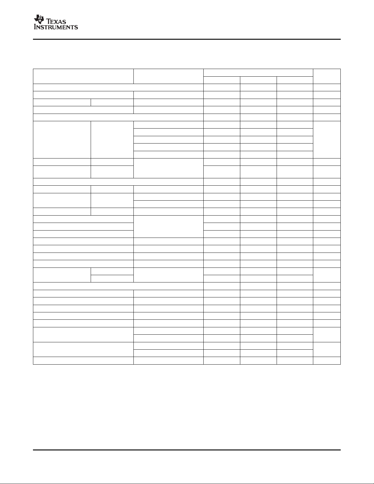
ELECTRICAL CHARACTERISTICS
Limit specifications at – 40 ° C to +85 ° C, typical specifications at +25 ° C, AVDD = +2.5V, AVSS = – 2.5V, f
VREFN = – 2.5V, DVDD = +3.3V, and f
PARAMETER CONDITIONS MIN TYP MAX UNIT
ANALOG INPUTS
Full-scale input voltage VIN= AINP – AINN ± V
Absolute input range AINP or AINN AVSS – 0.1 AVDD + 0.1 V
Differential input impedance 55 k Ω
AC PERFORMANCE
Signal-to-noise ratio
(2)
Total harmonic distortion THD – 122 – 115 dB
Spurious-free dynamic
(3)
range
DC PERFORMANCE
Resolution No missing codes 31 Bits
Data rate f
Integral nonlinearity
(4)
Offset error 10 200 µ V
Offset error after calibration
(6)
Offset drift 0.06 µ V/ ° C
Gain error 0.1 0.3 %
Gain error after calibration
(6)
Gain drift 0.4 ppm/ ° C
Common-mode rejection fCM= 60Hz 105 120 dB
Power-supply rejection fPS= 60Hz dB
AVDD, AVSS 85 95
FIR DIGITAL FILTER RESPONSE
Passband ripple ± 0.003 dB
Passband ( – 0.01dB) 0.375 × f
Stop band attenuation
(7)
Stop band 0.500 × f
Bandwidth ( – 3dB) 0.413 × f
Group delay s
Settling time (latency) s
High-pass filter corner 0.1 10 Hz
(1) f
(2) SNR = signal-to-noise ratio = 20 log (V
= system clock.
CLK
(3) Highest spurious component including harmonics.
= 1000SPS, unless otherwise noted.
DATA
f
= 250SPS 130
DATA
f
= 500SPS 127
DATA
SNR f
SFDR 123 dB
DATA
VIN= 31.25Hz, – 0.5dBFS
= 1000SPS 120 124 dB
DATA
f
= 2000SPS 121
DATA
f
= 4000SPS 118
DATA
FIR filter mode 250 4000 SPS
Sinc filter mode 8,000 128,000 SPS
INL Differential input 0.00006 0.0005 % FSR
Shorted input 1 µ V
DVDD 85 105
135 dB
FIR filter, minimum phase 5/f
FIR filter, linear phase 31/f
FIR filter, minimum phase 10/f
FIR filter, linear phase 62/f
Full-Scale/V
RMS
RMS
Noise), VIN= 20mV
.
DC
(4) Best-fit method.
(5) FSR: Full-scale range = ± V
(6) Calibration accuracy is on the level of noise reduced by 4 (calibration averages 16 readings).
(7) Input frequencies in the range of Nf
ranges intermodulation = 120dB, typ.
/2.
REF
CLK
/512 ± f
/2 (N = 1, 2, 3...) can mix with the modulator chopping clock. In these frequency
DATA
(1)
= 4.096MHz, VREFP = +2.5V,
CLK
ADS1281
/2 V
REF
0.0002 %
DATA
DATA
DATA
DATA
DATA
DATA
DATA
(5)
Hz
Hz
Hz
Copyright © 2007, Texas Instruments Incorporated Submit Documentation Feedback 3
Product Folder Link(s): ADS1281
Page 4
www.ti.com
ADS1281
SBAS378A – SEPTEMBER 2007 – REVISED NOVEMBER 2007
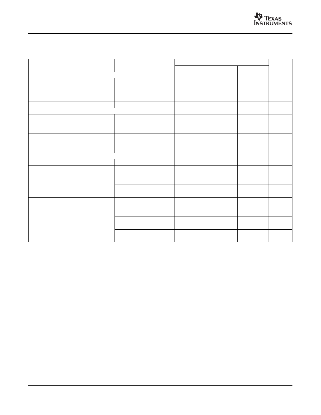
ELECTRICAL CHARACTERISTICS (continued)
Limit specifications at – 40 ° C to +85 ° C, typical specifications at +25 ° C, AVDD = +2.5V, AVSS = – 2.5V, f
VREFN = – 2.5V, DVDD = +3.3V, and f
PARAMETER CONDITIONS MIN TYP MAX UNIT
VOLTAGE REFERENCE INPUTS
Reference input voltage (AVDD – AVSS)
V
= VREFP – VREFN + 0.2
REF
Negative reference input VREFN AVSS – 0.1 VREFP – 0.5 V
Positive reference input VREFP VREFN + 0.5 AVDD + 0.1 V
Reference input impedance 85 k Ω
DIGITAL INPUT/OUTPUT
V
IH
V
IL
V
OH
V
OL
Input leakage 0 < V
Clock input f
POWER SUPPLY
AVSS – 2.6 0 V
AVDD AVSS + 4.75 AVSS + 5.25 V
DVDD 1.65 3.6 V
AVDD, AVSS current Standby mode 1 15 | µ A |
DVDD current
Power dissipation Standby mode 90 250 µ W
= 1000SPS, unless otherwise noted.
DATA
CLK
Power-Down mode 1 15 | µ A |
Power-Down mode
Power-Down mode 10 150 µ W
0.5 5 V
0.8 × DVDD DVDD V
DGND 0.2 × DVDD V
IOH= 1mA 0.8 × DVDD V
IOL= 1mA 0.2 × DVDD V
< DVDD ± 10 µ A
DIGITAL IN
1 4.096 MHz
Operating mode 2 3 | mA |
Operating mode 0.6 0.8 mA
Modulator mode 0.1 mA
Standby mode 25 50 µ A
(8)
Operating mode 12 18 mW
(8) CLK input stopped.
= 4.096MHz, VREFP = +2.5V,
CLK
ADS1281
1 15 µ A
4 Submit Documentation Feedback Copyright © 2007, Texas Instruments Incorporated
Product Folder Link(s): ADS1281
Page 5
www.ti.com
CLK
SCLK
DRDY
DOUT
MOD/DIN
DGND
PHS/MCLK
DR1/M1
DR0/M0
HPF/SYNC
MFLAG
DGND
BYPAS
DGND
DVDD
PINMODE
RESET
PWDN
VREFP
VREFN
AVSS
AVDD
AINN
AINP
1
2
3
4
5
6
7
8
9
10
11
12
24
23
22
21
20
19
18
17
16
15
14
13
ADS1281
ADS1281
SBAS378A – SEPTEMBER 2007 – REVISED NOVEMBER 2007
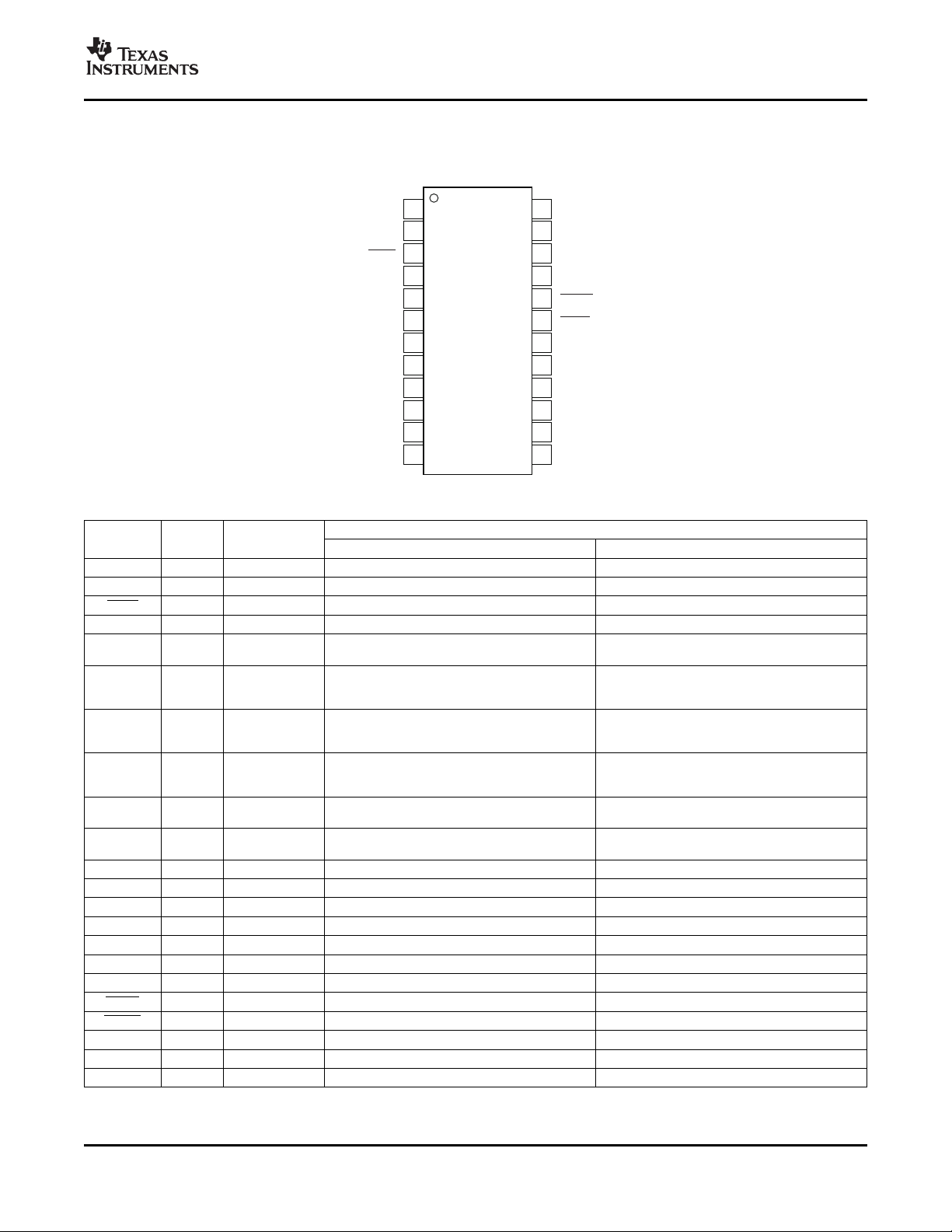
DEVICE INFORMATION
TSSOP-24
Top View
TERMINAL FUNCTIONS
DESCRIPTION
NAME NO. FUNCTION PIN MODE (PINMODE = 1) REGISTER MODE (PINMODE = 0)
CLK 1 Digital input Master clock input Master clock input
SCLK 2 Digital input SPI serial clock input SPI serial clock input
DRDY 3 Digital output Data ready output: read data on falling edge Data ready output: read data on falling edge
DOUT 4 Digital output SPI serial data output SPI serial data output
MOD/DIN 5 Digital input DIN: SPI serial data input
PHS/MCLK 7 Digital I/O 0 = Linear phase filter, 1 = Minimum phase filter MCLK: Modulator clock output
DR1/M1 8 Digital I/O M1: Modulator data output 1
DR0/M0 9 Digital I/O M0: Modulator data output 0
HPF/SYNC 10 Digital input SYNC: Synchronize input
(MOD = 0) HPF: 0 = High-pass filter off, 1 = HPF on
MFLAG 11 Digital output
DGND 6, 12, 23 Digital ground Digital ground, pin 12 is the key ground point Digital ground, pin 12 is the key ground point
AINP 13 Analog input Positive analog input Positive analog input
AINN 14 Analog input Negative analog input Negative analog input
AVDD 15 Analog supply Positive analog power supply Positive analog power supply
AVSS 16 Analog supply Negative analog power supply Negative analog power supply
VREFN 17 Analog input Negative reference input Negative reference input
VREFP 18 Analog input Positive reference input Positive reference input
PWDN 19 Digital input Power-down input, active low Power-down input, active low
RESET 20 Digital input Synchronize input Reset input
PINMODE 21 Digital input 1 = Pin mode 0 = Register mode
DVDD 22 Digital supply Digital power supply: +1.8V to +3.3V Digital power supply: +1.8V to +3.3V
BYPAS 24 Capacitor bypass Digital core bypass; 1 µ F bypass capacitor to GND Digital core bypass; 1 µ F bypass capacitor to GND
Copyright © 2007, Texas Instruments Incorporated Submit Documentation Feedback 5
MOD: 0 = Digital filter mode
1 = Filter bypass (modulator output)
(MOD = 0) PHS: If in modulator mode:
(MOD = 1) MCLK: Modulator clock output Otherwise, the pin is an unused input (must be tied).
(MOD = 0) DR1 = Data rate select input 1
(MOD = 1) M1 = Modulator data output 1
(MOD = 0) DR0 = Data rate select input 0
(MOD = 1) M0 = Modulator data output 0
Otherwise, the pin is an unused input (must be tied).
Otherwise, the pin is an unused input (must be tied).
If in modulator mode:
If in modulator mode:
(MOD = 1) SYNC = Synchronize Input
Modulator over-range flag: Modulator over-range flag:
0 = Normal, 1 = Modulator over-range 0 = Normal, 1 = Modulator over-range
Product Folder Link(s): ADS1281
Page 6
www.ti.com
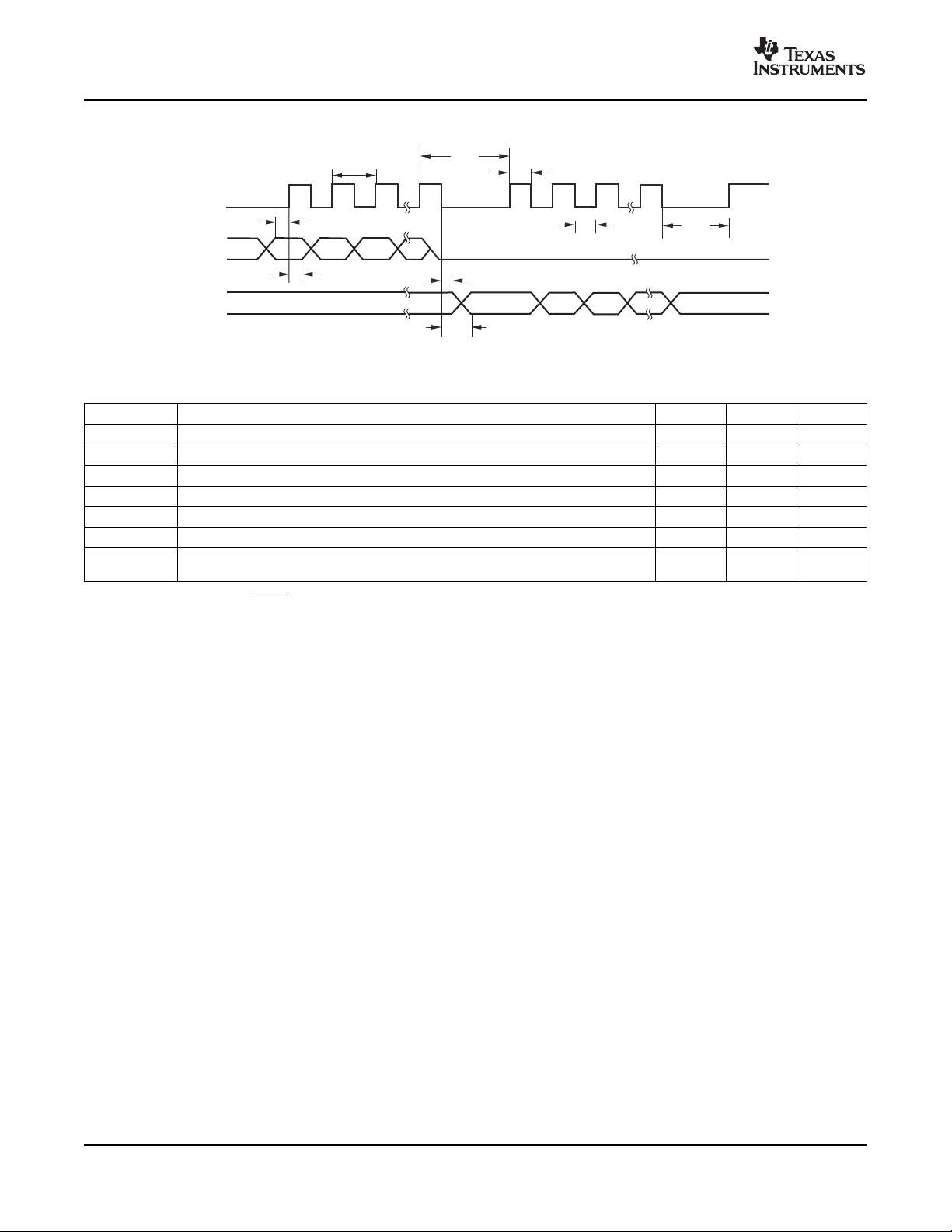
SCLK
DIN
DOUT
t
SCLK
t
SPWH
t
SCDL
t
DIST
t
DIHD
t
SPWL
t
SCDL
t
DOHD
t
DOPD
ADS1281
SBAS378A – SEPTEMBER 2007 – REVISED NOVEMBER 2007
TIMING DIAGRAM
TIMING REQUIREMENTS
At TA= – 40 ° C to +85 ° C and DVDD = 1.65V to 3.6V, unless otherwise noted.
PARAMETER DESCRIPTION MIN MAX UNITS
t
SCLK
t
SPWH, L
t
DIST
t
DIHD
t
DOPD
t
DOHD
t
SCDL
(1) Holding SCLK low for 64 DRDY falling edges resets the SPI interface.
(2) Load on DOUT = 20pF || 100k Ω .
SCLK period 2 16 1/f
SCLK pulse width, high and low
(1)
0.8 10 1/f
DIN valid to SCLK rising edge: setup time 50 ns
Valid DIN to SCLK rising edge: hold time 50 ns
SCLK falling edge to valid new DOUT: propagation delay
(2)
SCLK falling edge to DOUT invalid: hold time 0 ns
Final SCLK rising edge of command to first SCLK rising edge for register read/write
data. (Also between consecutive commands.)
24 1/f
CLK
CLK
100 ns
CLK
6 Submit Documentation Feedback Copyright © 2007, Texas Instruments Incorporated
Product Folder Link(s): ADS1281
Page 7
www.ti.com
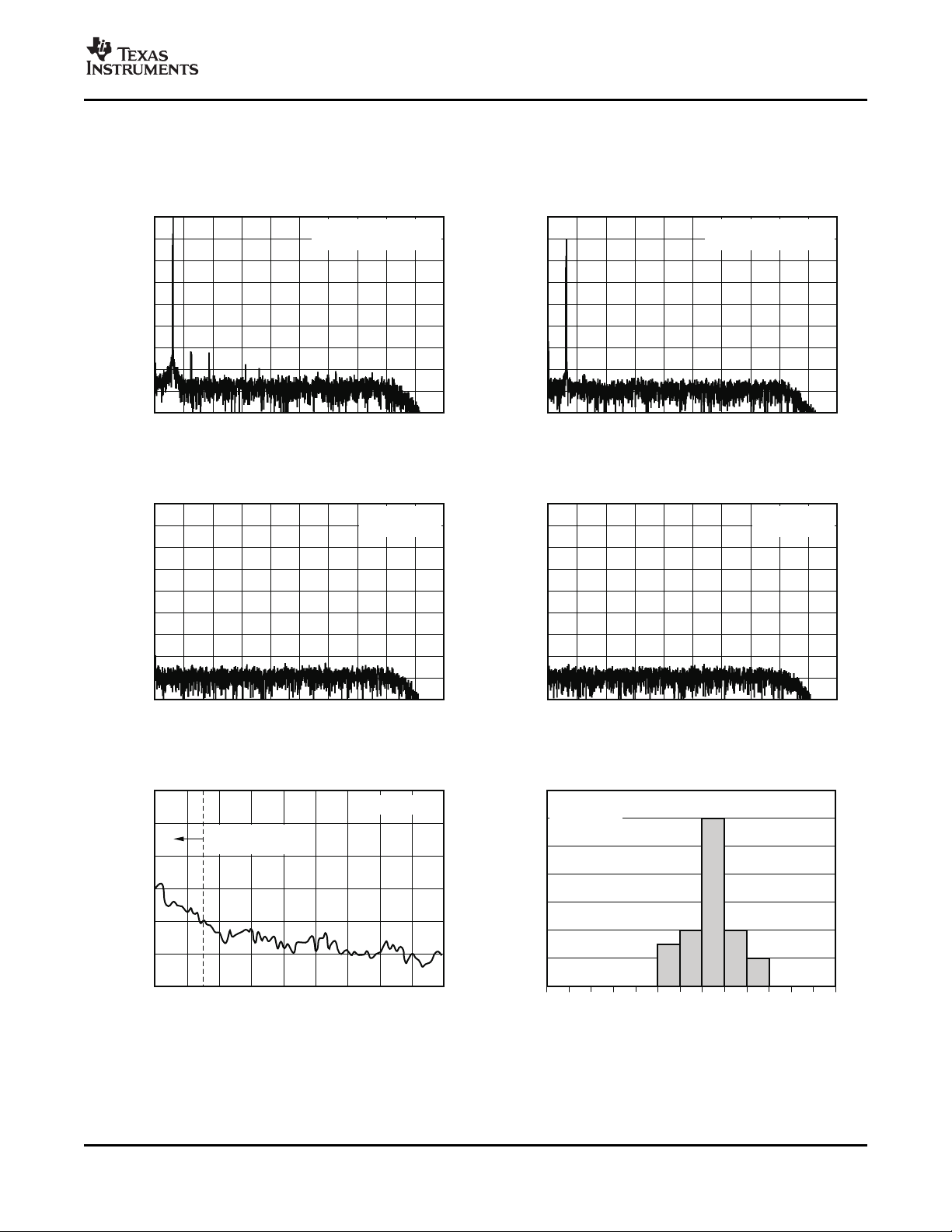
TYPICAL CHARACTERISTICS
0 50
Frequency(Hz)
0
-20
-40
-60
-80
-180
Amplitude(dB)
100 150 500250 350 450200 300 400
-100
-120
-140
-160
V = 0.5dBFS,31.25Hz
THD= 121.8dB
IN
-
-
0 50
Frequency(Hz)
0
-20
-40
-60
-80
-180
Amplitude(dB)
100 150 500250 350 450200 300 400
-100
-120
-140
-160
V = 20dBFS,31.25Hz
THD= 120.1dB
IN
-
-
0 50
Frequency(Hz)
0
-20
-40
-60
-80
-180
Amplitude(dB)
100 150 500250 350 450200 300 400
-100
-120
-140
-160
ShortedInput
SNR=124.1dB
0 50
Frequency(Hz)
0
-20
-40
-60
-80
-180
Amplitude(dB)
100 150 500250 350 450200 300 400
-100
-120
-140
-160
V =20mV
SNR=124.3dB
IN DC
10 20
InputFrequency(Hz)
-100
-105
-110
-115
-120
-130
THD(dB)
30 40 10060 8050 70 90
-125
THDLimitedby
SignalGenerator
V = 0.5dBFS-
IN
122.00
SNR(dB)
14
12
10
8
0
Occurences
6
4
122.50
123.00
123.50
124.00
124.50
125.00
122.25
122.75
123.25
123.75
124.25
124.75
2
25Units
ShortedInput
At TA= +25 ° C, AVDD = +2.5V, AVSS = – 2.5V, f
f
= 1000SPS, unless otherwise noted.
DATA
OUTPUT SPECTRUM OUTPUT SPECTRUM
Figure 1. Figure 2.
SBAS378A – SEPTEMBER 2007 – REVISED NOVEMBER 2007
= 4.096MHz, VREFP = +2.5V, VREFN = – 2.5V, DVDD = +3.3V, and
CLK
ADS1281
OUTPUT SPECTRUM OUTPUT SPECTRUM
Figure 3. Figure 4.
THD vs INPUT FREQUENCY SNR HISTOGRAM
Copyright © 2007, Texas Instruments Incorporated Submit Documentation Feedback 7
Figure 5. Figure 6.
Product Folder Link(s): ADS1281
Page 8
www.ti.com
-55 -35
Temperature( C)°
125
124
123
122
121
120
SNR(dB)
-15 5 12545 8525 65 105
SNR:ShortedInput
THD:V =31.25Hz, 0.5dBFS-
IN
-115
-117
-119
-121
-123
-125
THD(dB)
0 1
V (V)
REF
6
5
4
0
Noise( V
)
m
R
MS
2 3 654
3
-105
-110
-115
-135
THD(dB)
-120
Noise:ShortedInput
THD:V =31.25Hz, 0.5dBFS-
IN
2 -125
1 -130
1.0 1.5
f (MHz)
CLK
125
123
121
117
SNR(dB)
2.0 2.5 4.53.53.0 4.0
119
-105
-110
-115
-125
THD(dB)
-120
SNR:ShortedInput
THD:V =31.25Hz, 0.5dBFS-
IN
DataRate=f /4096
CLK
10 100
PowerSupplyandCommon-ModeFrequency(Hz)
140
120
100
0
PSRandCMR(dB)
1k 10k 1M100k
80
CMR
AVDD
60
40
40
AVSS
DVDD
-2.5 -2.0
InputLevel(V)
3
2
1
0
-1
-3
LinearityError(ppm)
-1.5 -1.0 2.50 1.0 2.0-0.5 0.5 1.5
-2
IntegralNonlinearity= 0.5ppm±
-55 -35
Temperature( C)°
4
2
1
0
INL(ppm)
-15 5 1256525 85 105
3
45
16
8
4
0
Power(mW)
12
INL
Power
ADS1281
SBAS378A – SEPTEMBER 2007 – REVISED NOVEMBER 2007
TYPICAL CHARACTERISTICS (continued)
At TA= +25 ° C, AVDD = +2.5V, AVSS = – 2.5V, f
f
= 1000SPS, unless otherwise noted.
DATA
= 4.096MHz, VREFP = +2.5V, VREFN = – 2.5V, DVDD = +3.3V, and
CLK
SNR AND THD vs TEMPERATURE NOISE AND THD vs V
Figure 7. Figure 8.
POWER-SUPPLY AND COMMON-MODE REJECTION
SNR AND THD vs f
CLK
vs FREQUENCY
REF
Figure 9. Figure 10.
LINEARITY ERROR vs INPUT LEVEL INL AND POWER vs TEMPERATURE
8 Submit Documentation Feedback Copyright © 2007, Texas Instruments Incorporated
Figure 11. Figure 12.
Product Folder Link(s): ADS1281
Page 9
www.ti.com
-55 -35
Temperature( C)°
200
100
0
-100
-200
-400
NormalizedGainError(ppm)
-15 5 12545 8525 65 105
-300
GainError
5Units
Offset
100
75
50
25
0
-50
NormalizedOffset(
V)
m
-25
0 0.5
f (MHz)
CLK
16
14
12
10
8
0
Power(mW)
1.0 1.5 4.52.5 3.52.0 3.0 4.0
6
4
2
-100
Offset( V)m
10
9
7
5
0
Occurences
3
2
-80
-60
-40
-20
0
20
40
60
80
100
-
90
-70
-50
-30
-10
10
30
50
70
90
25Units
-0.50
GainError(%)
18
16
14
12
10
8
0
Occurences
6
2
4
-0.40
-0.30
-0.20
-0.10
0
0.10
0.20
0.30
0.40
0.50
-0.45
-0.35
-0.25
-0.15
-0.05
0.05
0.15
0.25
0.35
0.45
25Units
-1.0
OffsetDrift( V/ C)m °
90
80
70
60
50
40
0
Occurences
30
10
20
-0.8
-0.6
-0.4
-0.2
0
0.2
0.4
0.6
0.8
1.0
-
0.9
-0.7
-0.5
-0.3
-
0.1
0.1
0.3
0.5
0.7
0.9
25Units
Basedon20 C
IntervalsOvertheRange
40 Cto+85 C.
°
°- °
-2.0
GainDrift(ppm/ C)°
50
45
40
35
30
25
0
Occurences
20
10
15
5
-1.6
-1.2
-0.8
-0.4
0
0.4
0.8
1.2
1.6
2.0
-
1.8
-1.4
-1.0
-0.6
-
0.2
0.2
0.6
1.0
1.4
1.8
25Units
Basedon20 CIntervals
OvertheRange
40 Cto+85 C.
°
° °-
TYPICAL CHARACTERISTICS (continued)
At TA= +25 ° C, AVDD = +2.5V, AVSS = – 2.5V, f
f
= 1000SPS, unless otherwise noted.
DATA
SBAS378A – SEPTEMBER 2007 – REVISED NOVEMBER 2007
= 4.096MHz, VREFP = +2.5V, VREFN = – 2.5V, DVDD = +3.3V, and
CLK
ADS1281
POWER vs f
CLK
GAIN AND OFFSET vs TEMPERATURE
Figure 13. Figure 14.
OFFSET HISTOGRAM GAIN ERROR HISTOGRAM
Copyright © 2007, Texas Instruments Incorporated Submit Documentation Feedback 9
Figure 15. Figure 16.
OFFSET DRIFT HISTOGRAM GAIN DRIFT HISTOGRAM
Figure 17. Figure 18.
Product Folder Link(s): ADS1281
Page 10
www.ti.com
4th-Order
DS
Modulator
Programmable
DigitalFilter
Serial
Interface
Calibration
Control
AINP
AVDD
AVSS
DVDDCLK
DGND
HPF/SYNC
AINN
VREFN
MFLAG
VREFP
ADS1281
RESET
PINMODE
PWDN
Over-Range
Detection
MOD/DIN
DOUT
DRDY
SCLK
LDO
PHS/MCLK
DR0/M0
DR1/M1
+1.8V
(DigitalCore)
BYPAS
ADS1281
SBAS378A – SEPTEMBER 2007 – REVISED NOVEMBER 2007
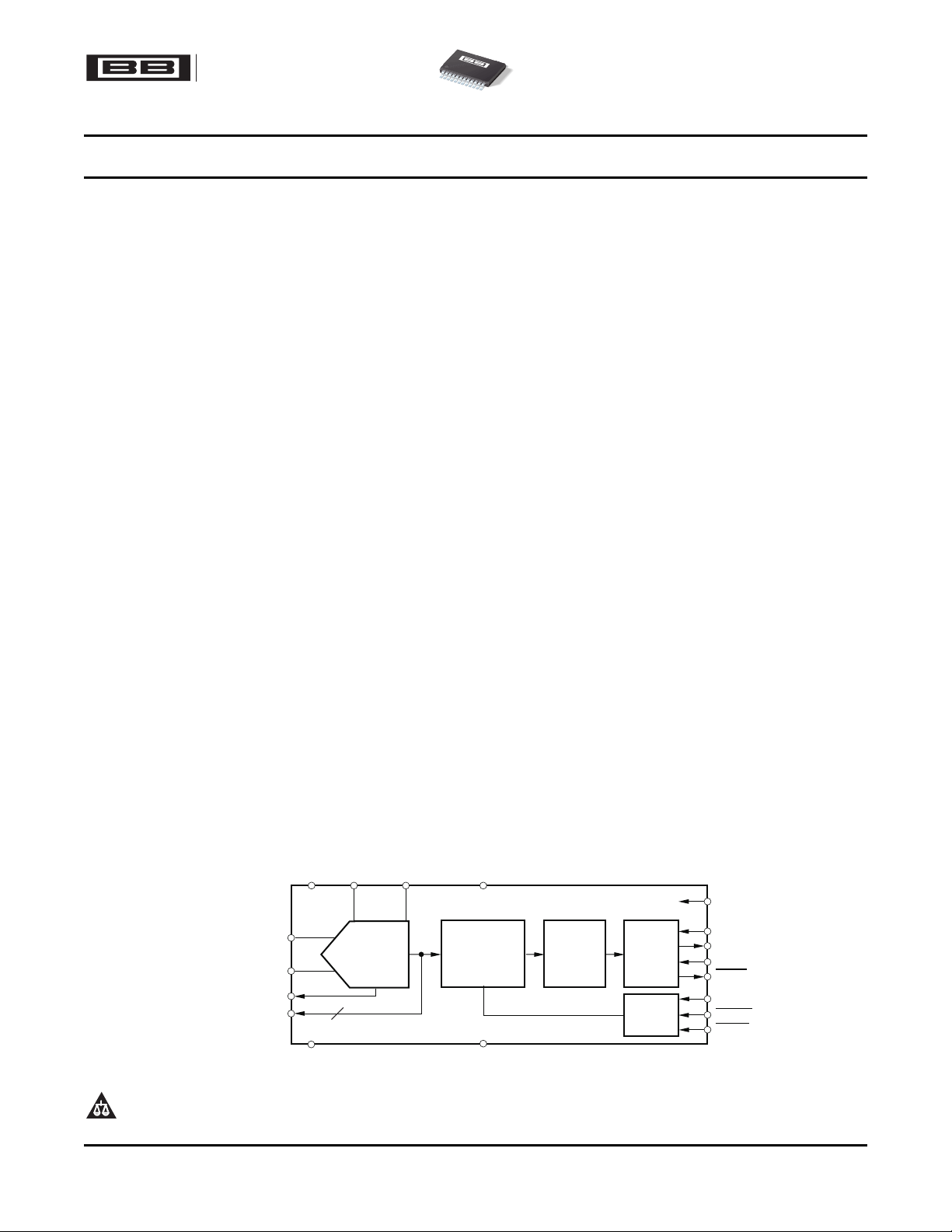
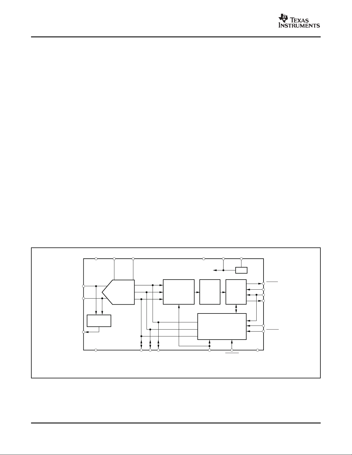
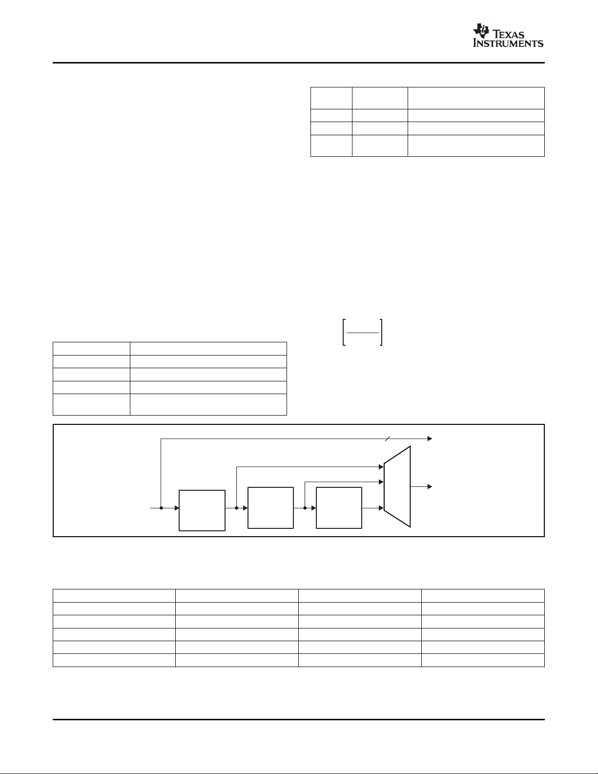
OVERVIEW
The ADS1281 is a high-performance analog-to-digital The digital filter is comprised of a variable decimation
converter (ADC) intended for energy exploration, rate, fifth-order sinc filter followed by a
seismic monitoring, chromatography, and other decimate-by-32, FIR low-pass filter with
exacting applications. The converter provides 24- or programmable phase, and then by an adjustable
32-bit output data in data rates from 4000SPS to high-pass filter for dc removal of the output reading.
250SPS. The output of the digital filter can be taken from the
Figure 19 shows the block diagram of the ADS1281.
The device features unipolar and bipolar analog Gain and offset registers scale the digital filter output
power supplies (AVDD and AVSS, respectively) for to produce the final code value. The scaling feature
input range flexibility and a digital supply accepting can be used for calibration and sensor gain matching.
1.8V to 3.3V. The analog supplies may be set to +5V The output data are provided with either a 24-bit word
to accept unipolar signals (with input offset) or set or a full 32-bit word, allowing full utilization of the
lower in the range of ± 2.5V to accept true bipolar inherently high resolution.
input signals (ground referenced).
An internal low-dropout (LDO) regulator is used to device: Pin control or Register control. In Pin control
power the digital core from DVDD. The BYPAS pin is mode, the device is controlled by simple pin settings;
the LDO output and requires a 0.1 µ F capacitor for there are no registers to program. In Register control
noise reduction (BYPAS should not be used to drive mode, the device is controlled by register settings.
external circuitry). The functionality of several device pins depends on
The inherently-stable, fourth-order, Δ Σ modulator
measures the differential input signal V
= (AINP –
IN
AINN) against the differential reference The SYNC input resets the operation of both the
V
= (VREFP – VREFN). A digital output (MFLAG) digital filter and the modulator, allowing synchronized
REF
indicates that the modulator is in over-range resulting conversions of multiple ADS1281 devices to an
from an input overdrive condition. The modulator external event. The SYNC input supports a
output is available directly on the MCLK, M0, and M1 continuously-toggled input mode that accepts an
output pins. The modulator connects to an on-chip external data frame clock locked to an integer of the
digital filter that provides the output code readings. conversion rate.
sinc, the FIR low-pass, or the IIR high-pass section.
The PINMODE input pin determines the mode of the
the control mode selected (see the Pin and Register
Modes section).
Figure 19. ADS1281 Block Diagram
10 Submit Documentation Feedback Copyright © 2007, Texas Instruments Incorporated
Product Folder Link(s): ADS1281
Page 11
www.ti.com
2nd-Order
2nd-Stage
DS
2nd-Order
1st-Stage
DS
AnalogInput(V )
IN
4th-OrderModulator
PHS/MCLK
DR0/M0
DR1/M1
f
CLK
/4
Y[n]=3M0[n 2] 6M0[n 3]+4M0[n 4]
+9(M1[n] 2M1[n 1]+M1[n 2])
- - - -
- - -
ADS1281
SBAS378A – SEPTEMBER 2007 – REVISED NOVEMBER 2007
The RESET input resets the register settings
(Register mode) and also restarts the conversion
process.
MODULATOR
The high-performance modulator is an
inherently-stable, fourth-order, Δ Σ , 2 + 2 pipelined
The PWDN input sets the device into a micro-power structure, as shown in Figure 20 . It shifts the
state. Note that register settings are not retained in quantization noise to a higher frequency (out of the
PWDN mode. Use the STANDBY command in its passband) where digital filtering can easily remove it.
place if it is desired to retain register settings (the The modulator can be filtered either by the on-chip
quiescent current in the Standby mode is slightly digital filter or by use of post-processing filters.
higher).
Noise-immune Schmitt-trigger and clock-qualified
inputs ( RESET and SYNC) provide increased
reliability in high-noise environments.
The serial interface is used to read conversion data,
in addition to reading from and writing to the
configuration registers.
NOISE PERFORMANCE
The ADS1281 offers outstanding noise performance
(SFDR). Table 1 summarizes the typical noise
performance.
Table 1. Noise Performance (Typical)
DATA RATE FILTER – 3dB BW (Hz) SNR (dB)
250 FIR 103 130
500 FIR 206 127
1000 FIR 413 124
2000 FIR 826 121
4000 FIR 1652 118
(1) VIN= 20mV
.
DC
(1)
IDLE TONES
The ADS1281 modulator incorporates an internal
dither signal that randomizes the idle tone energy.
Low-level idle tones may still be present, typically
– 137dB below full-scale. The low-level idle tones can
be shifted out of the passband with the application of
an external 20mV offset.
The modulator first stage converts the analog input
voltage into a pulse-code modulated (PCM) stream.
When the level of differential analog input (AINP –
AINN) is near one-half the level of the reference
voltage 1/2 × (VREFP – VREFN), the ‘ 1 ’ density of
the PCM data stream is at its highest. When the level
of the differential analog input is near zero, the PCM
‘ 0 ’ and ‘ 1 ’ densities are nearly equal. At the two
extremes of the analog input levels (+FS and – FS),
the ‘ 1 ’ density of the PCM streams are approximately
+90% and +10%, respectively.
The modulator second stage produces a '1' density
data stream designed to cancel the quantization
noise of the first stage. The data streams of the two
stages are then combined before input to the digital
filter stage, as shown in Equation 1 .
Figure 20. Fourth-Order Modulator
ADC
The ADC block of the ADS1281 is composed of two
blocks: a high-accuracy modulator and a
programmable digital filter.
Copyright © 2007, Texas Instruments Incorporated Submit Documentation Feedback 11
(1)
M0[n] represents the most recent first-stage output
while M0[n – 1] is the previous first-stage output.
When the modulator output is enabled, the digital
filter shuts down to save power.
Product Folder Link(s): ADS1281
Page 12
www.ti.com
Amplitude(dB)
Frequency(Hz)
0
-20
-40
-60
-80
-100
-180
1 10
100 100k
1k 10k
-120
-140
-160
1HzResolution
V =20mV
IN DC
f
MOD
/2
MFLAG
100%FS
AINN
AINP
P
Q
IABSI
å
ThresholdTolerance: 2.5%Typical±
ADS1281
SBAS378A – SEPTEMBER 2007 – REVISED NOVEMBER 2007
The modulator is optimized for input signals within a If the inputs are sufficiently overdriven to drive the
4kHz passband. As Figure 21 shows, the noise modulator to full duty cycle, all 1s or all 0s
shaping of the modulator results in a sharp increase ( ± 110%FSR), the modulator enters a stable saturated
in noise above 6kHz. The modulator has a chopped state. The digital output code may clip to +FS or – FS,
input structure that further reduces noise within the again depending on the duration. A small duration
passband. The noise is moved out of the passband overdrive may not always clip the output code. When
and appears at the chopping frequency (f
8kHz). The component at 6.5kHz is the tone requires up to 12 modulator clock cycles (f
frequency, shifted out of band by a 20mV external saturation and return to the linear region. The digital
input. The frequency of the tone is approximately filter requires an additional 62 conversion for fully
V
/3 (in kHz). settled data (linear phase FIR).
IN
/512 = the input returns to the normal range, the modulator
CLK
In the extreme case of over-range, either input is
overdriven exceeding that either analog supply
voltage plus an internal ESD diode drop. The internal
ESD diodes begin to conduct and the signal on the
input is clipped. If the differential input signal range is
not exceeded, the modulator remains in linear
operation. If the differential input signal range is
exceeded, the modulator is saturated but stable, and
outputs all 1s or 0s. When the input overdrive is
removed, the diodes recovery quickly and the
ADS1281 recovers as normal. Note that the linear
input range is ± 100mV beyond the analog supply
voltages; with input levels above this, use care to limit
the input current to 100mA peak transient and 10mA
continuous.
) to exit
MOD
Figure 21. Modulator Output Spectrum
MODULATOR OVER-RANGE DETECTION (MFLAG)
MODULATOR OVER-RANGE
The ADS1281 modulator is inherently stable and,
therefore, has predictable recovery behavior that
results from an input overdrive condition. The
modulator does not exhibit self-resetting behavior,
which often results in an unstable output data stream.
The ADS1281 modulator outputs a 1s density data
stream at 90% duty cycle with the positive full-scale
input signal applied (10% duty cycle with the negative
full-scale signal). If the input is overdriven past 90%
modulation, but below 100% modulation (10% and
0% for negative overdrive, respectively), the
modulator remains stable and continues to output the
1s density data stream. The digital filter may or may
not clip the output codes to +FS or – FS, depending
on the duration of the overdrive. When the input is
returned to the normal range from a long duration
overdrive (worst case), the modulator returns
immediately to the normal range, but the group delay
of the digital filter delays the return of the conversion
result to within the linear range (31 readings for linear
phase FIR). 31 additional readings (62 total) are
required for completely settled data.
12 Submit Documentation Feedback Copyright © 2007, Texas Instruments Incorporated
Product Folder Link(s): ADS1281
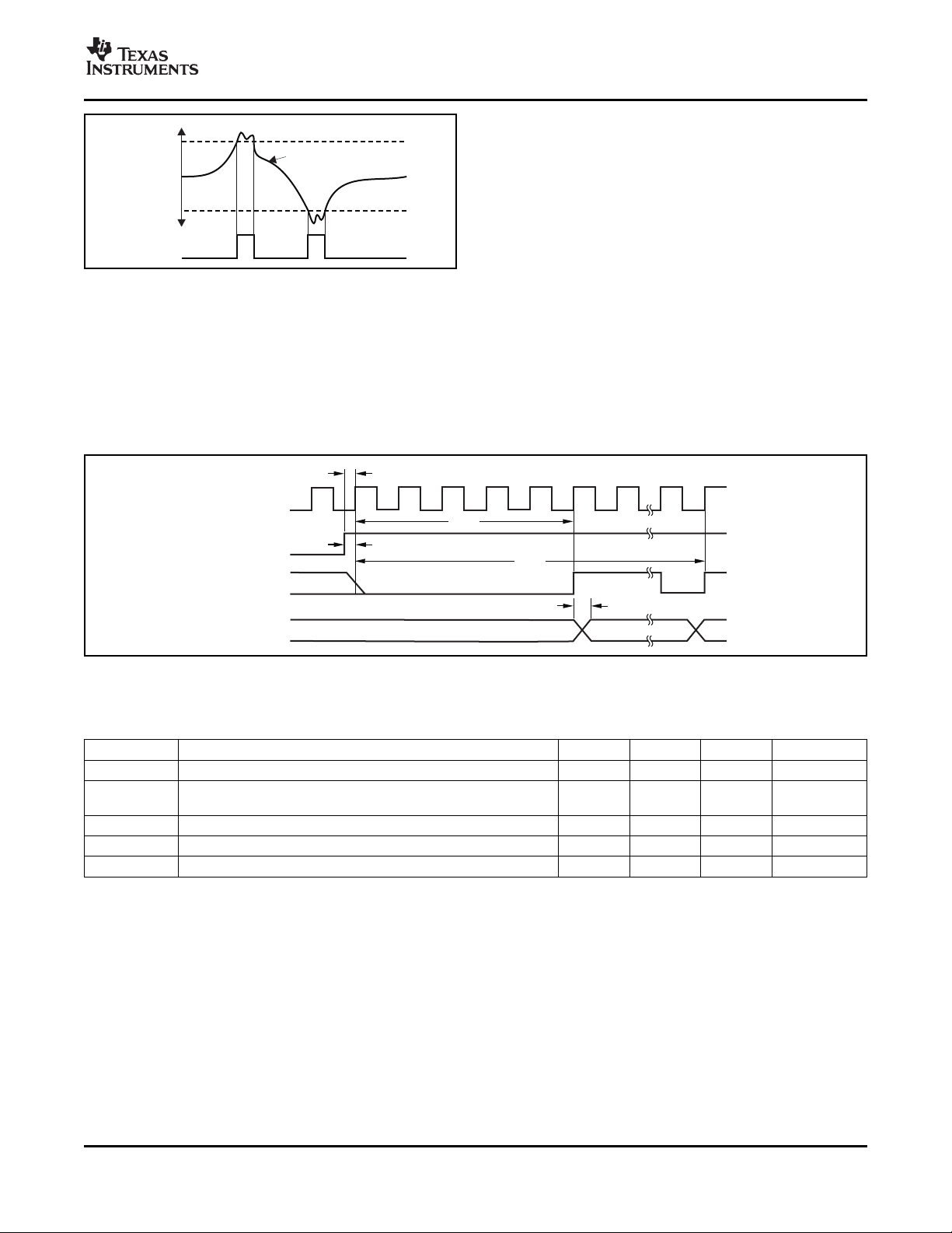
The ADS1281 has a fast-responding over-range
detection, indicating when the differential input
exceeds approximately 100% over-range. The
threshold tolerance is ± 2.5%.The MFLAG output
asserts high when in an over-range condition. As
Figure 22 and Figure 23 illustrate, the absolute value
of the input is compared to 100% of range. The
output of the comparator is sampled at the rate of
f
/2, yielding the MFLAG output. The minimum
MOD
MFLAG pulse width is f
/2.
MOD
Figure 22. Modulator Over-Range Block Diagram
Page 13
www.ti.com
MFLAG
+100%
(AINP AINN)-
-100%
0%
CLK
SYNC
PHS/MCLK
DR0/M0
DR1/M1
t
MCM0, 1
(MCLK=CLK/4)
t
SCSU
t
CSHD
t
CMD
1 2 543
t
SYMD
Figure 23. Modulator Over-Range Flag Operation (f
MODULATOR OUTPUT MODE
The modulator digital stream output is available
directly, bypassing and disabling the internal digital
filter. The modulator output mode is activated in the
Pin mode by setting MOD/DIN = 1, and in Register
mode by setting the CONFIG0 register bits
ADS1281
SBAS378A – SEPTEMBER 2007 – REVISED NOVEMBER 2007
FILTR[1:0] = 00. Pins DR0/M0 and DR1/M1 then
become the modulator data outputs and the
PHS/MCLK becomes the modulator clock output.
When not in the modulator mode, these pins are
inputs and must not float.
The modulator output is composed of three signals:
one output for the modulator clock (PHS/MCLK) and
two outputs for the modulator data (DR0/M0 and
DR1/M1). The modulator clock output rate is f
/4). The SYNC input resets the MODCLK phase,
CLK
as shown in Figure 24 . The SYNC input is latched on
the rising edge of CLK. The MODCLK resets and the
next rising edge of MODCLK occurs five CLK periods
later.
The modulator output data are two bits wide, which
must be merged together before being filtered. Use
the time domain equation of Equation 1 to merge the
data outputs.
MOD
Figure 24. Modulator Mode Timing
Modulator Output Timing for Figure 24
PARAMETER DESCRIPTION MIN TYP MAX UNIT
t
MCD0, 1
t
CMD
t
CSHD
t
SCSU
t
SYMD
(1) Load on M0 and M1 = 20pF || 100k Ω .
Copyright © 2007, Texas Instruments Incorporated Submit Documentation Feedback 13
MODCLK rising edge to M0, M1 valid propagation delay
CLK rising edge (after SYNC rising edge) to MODCLK rising edge
reset time
CLK to SYNC hold time to not latch on CLK edge 10 ns
SYNC to CLK setup time to latch on CLK edge 10 ns
SYNC to stable bit stream 16 1/f
Product Folder Link(s): ADS1281
(1)
5 1/f
100 ns
CLK
MOD
Page 14
www.ti.com
H(Z)=
1 Z-
N
1 Z-
-1
5
SincFilter
Decimateby
8to128
FIRFilter
Decimate
by32
High-Pass
Filter
(IIR)
Filter
MUX
ToCalibrationBlock
FromModulator
DirectModulator
BitStream
3
ADS1281
SBAS378A – SEPTEMBER 2007 – REVISED NOVEMBER 2007
DIGITAL FILTER
The digital filter receives the modulator output and
decimates the data stream. By adjusting the amount
of filtering, tradeoffs can be made between resolution
Table 3. Digital Filter Selection, Pin Mode
MOD/DIN HPF/SYNC
PIN PIN DIGITAL FILTERS SELECTED
1 X Bypass; modulator output mode
and data rate: filter more for higher resolution, filter 0 0 Sinc + FIR
less for higher data rate.
The digital filter is comprised of three cascaded filter
0 1
Sinc + FIR + HPF
(low-pass and high-pass)
stages: a variable-decimation, fifth-order sinc filter; a
fixed-decimation FIR, low-pass filter (LPF) with
selectable phase; and a programmable, first-order,
high-pass filter (HPF), as shown in Figure 25 .
The output can be taken from one of the three filter
blocks, as shown in Figure 25 . To implement the
digital filter completely off-chip, select the filter bypass
setting (modulator output). For partial filtering by the
ADS1281, select the sinc filter output. For complete
on-chip filtering, activate both the sinc and FIR
stages. The HPF can then be included to remove dc
and low frequencies from the data. Table 2 shows the
filter options in Register mode. Table 3 shows the
Sinc Filter Stage (sinx/x)
The sinc filter is a variable decimation rate, fifth-order,
low-pass filter. Data are supplied to this section of the
filter from the modulator at the rate of f
The sinc filter attenuates the high-frequency noise of
the modulator, then decimates the data stream into
parallel data. The decimation rate affects the overall
data rate of the converter; it is set by the DR[1:0] and
MODE selections, as shown in Table 4 .
Equation 2 shows the scaled Z-domain transfer
function of the sinc filter.
filter options in Pin mode.
Table 2. Digital Filter Selection, Register Mode
FILTR[1:0] BITS DIGITAL FILTERS SELECTED
00 Bypass; modulator output mode
01 Sinc
10 Sinc + FIR
11
Sinc + FIR + HPF
(low-pass and high-pass)
(f
MOD
/4).
CLK
(2)
Figure 25. Digital Filter
Table 4. Sinc Filter Data Rates (CLK = 4.096MHz)
DR[1:0] PINS DR[2:0] REGISTER DECIMATION RATIO (N) SINC DATA RATE (SPS)
00 000 128 8,000
01 001 64 16,000
10 010 32 32,000
11 011 16 64,000
— 100 8 128,000
14 Submit Documentation Feedback Copyright © 2007, Texas Instruments Incorporated
Product Folder Link(s): ADS1281
Page 15

www.ti.com
½H =
(f)
½
5
sin
N4 f´p
f
CLK
Nsin
4 fp
f
CLK
Gain(dB)
NormalizedFrequency(f /f )
IN DATA
0
-0.5
-1.0
-1.5
-2.0
-2.5
-3.0
0 0.05
0.10 0.20
0.15
0 1 2
NormalizedFrequency(f /f )
IN DATA
0
-20
-40
-60
-80
-100
-120
-140
Gain(dB)
3 4 5
Output
FIRStage2
Decimateby2
FIRStage1
Decimateby2
Sinc
Filter
FIRStage4
Decimateby2
FIRStage3
Decimateby4
Linear
Minimum
PHASESelect
Coefficients
The frequency domain transfer function of the sinc
filter is shown in Equation 3 .
where:
N = decimation ratio (see Table 4 )
The sinc filter has notches (or zeroes) that occur at
the output data rate and multiples thereof. At these
frequencies, the filter has zero gain. Figure 26 shows
the frequency response of the sinc filter and
Figure 27 shows the roll-off of the sinc filter.
Figure 26. Sinc Filter Frequency Response
ADS1281
SBAS378A – SEPTEMBER 2007 – REVISED NOVEMBER 2007
(3)
Figure 27. Sinc Filter Roll-Off
FIR Stage
The second stage of the ADS1281 digital filter is an
FIR low-pass filter. Data are supplied to this stage
from the sinc filter. The FIR stage is segmented into
four sub-stages, as shown in Figure 28 . The first two
sub-stages are half-band filters with decimation ratios
of 2. The third sub-stage decimates by 4 and the
fourth sub-stage decimates by 2. The overall
decimation of the FIR stage is 32. Note that two
coefficient sets are used for the third and fourth
sections, depending on the phase selection. Table 23
in the Appendix section at the end of this document
lists the FIR stage coefficients. Table 5 lists the data
rates and overall decimation ratio of the FIR stage.
Table 5. FIR Filter Data Rates
DR[1:0] PINS DR[2:0] REGISTER DECIMATION RATIO (N) FIR DATA RATE (SPS)
00 000 4096 250
01 001 2048 500
10 010 1024 1000
11 011 512 2000
— 100 256 4000
Figure 28. FIR Filter Sub-Stages
Product Folder Link(s): ADS1281
Copyright © 2007, Texas Instruments Incorporated Submit Documentation Feedback 15
Page 16

www.ti.com
0 0.08
NormalizedInputFrequency(f /f )
IN DATA
0.003
0.002
0.001
0
- 10.00
- 20.00
- 30.00
Magnitude(dB)
0.16 0.24 0.32 0.40
0 5 10
TimeIndex(1/f )
DATA
1.4
1.2
1.0
0.8
0.6
0.4
0.2
0
-0.2
StepSize
15 20 25 30 35 40 45 50 55 60 65
LinearPhaseFilter
MinimumPhaseFilter
0.35 0.40 0.45
NormalizedInputFrequency(f /f )
IN DATA
0
-20
-40
-60
-80
-100
-140
Amplitude(dB)
0.65
-120
0.50 0.55 0.60
ADS1281
SBAS378A – SEPTEMBER 2007 – REVISED NOVEMBER 2007
As shown in Figure 29 , the FIR frequency response
provides a flat passband to 0.375 of the data rate
( ± 0.003dB passband ripple). Figure 30 shows the
transition from passband to stop band.
Figure 29. FIR Passband Amplitude Response
(f
= 500Hz)
DATA
GROUP DELAY AND STEP RESPONSE
The FIR block is implemented as a multi-stage FIR
structure with selectable linear or minimum phase
response. The passband, transition band, and stop
band responses of the filters are nearly identical but
differ in the respective phase responses.
Linear Phase Response
Linear phase filters exhibit constant delay time versus
input frequency (that is, constant group delay). Linear
phase filters have the property that the time delay
from any instant of the input signal to the same
instant of the output data is constant and is
independent of the signal nature. This filter behavior
results in essentially zero phase error when analyzing
multi-tone signals. However, the group delay and
settling time of the linear phase filter are somewhat
larger than the minimum phase filter, as shown in
Figure 31 .
Figure 31. FIR Step Response
Figure 30. FIR Transition Band Response
Although not shown in Figure 30 , the passband
response repeats at multiples of the modulator
frequency (Nf
MOD
– f0and Nf
+ f0, where N = 1, 2,
MOD
etc. and f0= passband). These image frequencies, if
present in the signal and not externally filtered, fold
back (or alias) into the passband and cause errors.
Placing an anti-alias, low-pass filter in front of the
ADS1281 inputs is recommended to limit possible
out-of-band input signals. Often, a single RC filter is
sufficient.
16 Submit Documentation Feedback Copyright © 2007, Texas Instruments Incorporated
Product Folder Link(s): ADS1281
Page 17

www.ti.com
Minimum Phase Response
HPF[dec]=65,536 1 -
cos +sin 1w -
N N
w
cos w
N
1 2-
0 20 40
Frequency(Hz)
35
30
25
20
15
10
5
GroupDelay(1/f
)
DATA
60 80 100 120 140 160 180 200
LinearPhaseFilter
MinimumPhaseFilter
HPF(Z)=
1 Z-
-1
1 bZ-
-1
2 a-
2
´
GainError(dB)
FrequencyRatio(f /f )
HP DATA
0
-0.10
-0.20
-0.30
-0.40
-0.50
0.0001 0.001
0.01 0.1
b=
( )1+(1 a)-
2
2
2
The minimum phase filter provides a short delay from
the arrival of an input signal to the output, but the
relationship (phase) is not constant versus frequency,
as shown in Figure 32 . The filter phase is selected by
the PHS bit (Register mode) or the PHS/MCLK pin
(Pin mode); Table 6 shows additional information.
Table 6. FIR Phase Selection
PHS BIT or
PHS/MCLK PIN FILTER PHASE
0 Linear
1 Minimum
ADS1281
SBAS378A – SEPTEMBER 2007 – REVISED NOVEMBER 2007
Where:
HPF = High-pass filter register value (converted
to hexidecimal)
ω
= 2 π fHP/f
N
radians)
fHP= High-pass corner frequency (Hz)
f
= Data rate (Hz)
DATA
Table 7. High-Pass Filter Value Examples
fHP(Hz) DATA RATE (SPS) HPF[1:0]
0.5 250 0337h
1.0 500 0337h
1.0 1000 019Ah
(1) In Pin Control mode the HPF value is fixed at 0332h.
The HPF causes a small gain error, in which case the
magnitude depends on the ratio of fHP/f
many common values of (f
negligible. Figure 33 shows the gain error of the HPF.
The gain error factor is illustrated in Equation 13 (see
the Appendix at the end of this document).
(normalized frequency,
DATA
/f
HP
), the gain error is
DATA
DATA
(6)
(1)
. For
Figure 32. FIR Group Delay (f
HPF Stage
The last stage of the ADS1281 filter block is a
first-order HPF implemented as an IIR structure. This
filter stage blocks dc signals and rolls off
low-frequency components below the cut-off
frequency. The transfer function for the filter is shown
in Equation 4 :
where b is calculated as shown in Equation 5 :
The high-pass corner frequency is programmed by
registers HPF[1:0], in hexidecimal. Equation 6 is used
to set the high-pass corner frequency. Table 7 lists
example values for the high-pass filter.
Copyright © 2007, Texas Instruments Incorporated Submit Documentation Feedback 17
= 500Hz)
DATA
(4)
Figure 33. HPF Gain Error
(5)
Product Folder Link(s): ADS1281
Page 18

www.ti.com
0.01 0.1
NormalizedFrequency(f/f )
C
0
-7.5
-15.0
-22.5
-30.0
-45.0
Amplitude(dB)
90
75
60
45
30
15
0
Phase( )°
1 10 100
Phase
Amplitude
-37.5
t
SAMPLE MOD
=1/f
ON
OFF
S
1
S
2
OFF
ON
S
1
S
1
AVSS+2.5V
R =R ||2R
AIN EFFB EFFA
AVSS+2.5V
R =325kW
EFFA
R =61kW
EFFB
(f =1.024MHz)
MOD
R =325kW
EFFA
AINN
AINP
C =3pF
A1
C =16pF
B
C =3pF
A2
S
2
AVSS+2.5V
S
2
AVSS+2.5V
AINN
AINP
Equivalent
Circuit
AVDD
AVSS
R =
EFF
f C´
MOD
X
1
ADS1281
SBAS378A – SEPTEMBER 2007 – REVISED NOVEMBER 2007
Figure 34 shows the first-order amplitude and phase
response of the HPF. Note that in the case of
applying step inputs or synchronizing, the settling
time of the filter should be taken into account.
ANALOG INPUT CIRCUITRY (AINP, AINN)
The ADS1281 measures the differential input signal
V
= (AINP – AINN) against the differential reference
IN
V
= (VREFP – VREFN) using internal capacitors
REF
that are continuously charged and discharged.
Figure 36 shows the simplified schematic of the ADC
input circuitry; the right side of the figure illustrates
the input circuitry with the capacitors and switches
replaced by an equivalent circuit. Figure 35
demonstrates the ON/OFF timings for the switches of
Figure 36 .
In Figure 36 , S
sampling phase. With switch S
to AINP, C
A2
(AINP – AINN). For the discharge phase, S
first and then S
approximately to AVSS + 1.3V and C
0V. This two-phase sample/discharge cycle repeats
with a period of t
frequency of the modulator. See the Master Clock
Input (CLK) section.
switches close during the input
1
closed, C
1
charges to AINN, and C
closes. C
2
SAMPLE
= 1/f
and C
A1
. f
MOD
MOD
A1
charges to
B
discharge to
A2
discharges to
B
is the operating
charges
opens
1
Figure 34. HPF Amplitude and Phase Response
Figure 35. S1and S2Switch Timing for Figure 36
Figure 36. Simplified ADC Input Structure
18 Submit Documentation Feedback Copyright © 2007, Texas Instruments Incorporated
Product Folder Link(s): ADS1281
Page 19

www.ti.com
AVSS 300mV<(AINPorAINN)<AVDD+300mV-
ESD
Diodes
ESD
Diodes
11.5pF
R W=85k
(f =1.024MHz)
EFF
MOD
AVDD
AVSS
VREFP
VREFN
R =
EFF
f C´
MOD
X
1
AVSS 300mV<(VREFPorVREFN)<AVDD+300mV-
SBAS378A – SEPTEMBER 2007 – REVISED NOVEMBER 2007
The charging of the input sampling capacitors draws
a transient current from the source driving the
ADS1281 ADC inputs. The average value of this
current can be used to calculate an effective
impedance (R
impedances scale inversely with f
f
is reduced by a factor of two, the impedances
MOD
EFF
) where R
= V
EFF
IN/IAVERAGE
. For example, if
MOD
. These
double.
ESD diodes protect the analog inputs. To keep these
diodes from turning on, make sure the voltages on
the input pins do not go below AVSS by more than
300mV, and likewise do not exceed AVDD by more
than 300mV, as shown in Equation 7 .
(7)
Some applications of the device may require external Figure 37. Simplified Reference Input Circuit
clamp diodes and/or series resistors to limit the input
voltage to within this range.
The ADS1281 reference inputs are protected by ESD
diodes. In order to prevent these diodes from turning
The ADS1281 is a very high-performance ADC. For
optimum performance, it is essential that the
on, the voltage on either input must stay within the
range shown in Equation 8 :
ADS1281 inputs be driven with a buffer with noise
and distortion commensurate with the ADS1281
performance; see the Applications section. Most
applications require an external capacitor (COG/NPO
dielectric) directly across the input pins. Depending
on the input driver settling characteristics, some
experimentation may be necessary to optimize the
value to minimize THD (generally in the range of
2.2nF to 100nF). Best performance is achieved with
the common-mode signal centered at mid-supply.
Although optimized for differential signals, the
ADS1281 inputs may be driven with a single-ended
A high-quality reference voltage is necessary for
achieving the best performance from the ADS1281.
Noise and drift on the reference degrade overall
system performance, and it is critical that special care
be given to the circuitry generating the reference
voltages in order to achieve full performance. For
most applications, a 1 µ F ceramic capacitor applied
directly to the reference inputs pins is suggested.
signal by fixing one input to mid-supply. To take
advantage of the full dynamic range, the driven input
must swing 5V
for V
PP
= 5V.
REF
VOLTAGE REFERENCE INPUTS (VREFP, VREFN)
The voltage reference for the ADS1281 ADC is the
differential voltage between VREFP and VREFN:
V
= VREFP – VREFN. The reference inputs use a
REF
structure similar to that of the analog inputs with the
circuitry on the reference inputs shown in Figure 37 .
The average load presented by the switched
capacitor reference input can be modeled with an
effective differential impedance of R
(t
SAMPLE
of the reference inputs loads an external reference
with non-zero source impedance.
= 1/f
). Note that the effective impedance
MOD
= t
EFF
/C
SAMPLE
IN
MASTER CLOCK INPUT (CLK)
The ADS1281 requires a clock input for operation.
The clock is applied to the CLK pin. The data
conversion rate scales directly with the CLK
frequency. Power consumption versus CLK frequency
is relatively constant (see the Typical Characteristics).
As with any high-speed data converter, a high-quality,
low-jitter clock is essential for optimum performance.
Crystal clock oscillators are the recommended clock
source. Make sure to avoid excess ringing on the
clock input; keep the clock trace as short as possible
and use a 50 Ω series resistor close to the source.
ADS1281
(8)
Copyright © 2007, Texas Instruments Incorporated Submit Documentation Feedback 19
Product Folder Link(s): ADS1281
Page 20

www.ti.com
ADS1281
SBAS378A – SEPTEMBER 2007 – REVISED NOVEMBER 2007
PIN AND REGISTER MODES
The PINMODE input (pin 21) is used to set the
control mode of the device: Pin mode or Register
mode. In Pin mode (PINMODE = 1), control of the
device is set by pins; there are no registers to
program. In Register mode, control of the device is
set by the configuration registers. As a result of the
increased flexibility provided by the register space,
Register mode has more control options. Table 8
describes the differences between the control modes.
Table 9 summarizes the functions of the dual-purpose
pins, depending on the control mode selected.
SYNCHRONIZATION (SYNC PIN AND SYNC COMMAND)
The ADS1281 can be synchronized to an external
event, as well as synchronized to other ADS1281
devices if the sync event is applied simultaneously to
all devices.
Table 8. Functions for Pin Mode and Register Mode
FUNCTION (PINMODE = 1) (PINMODE = 0)
Synchronization options Pulse only Continuous or Pulse
Digital filter options SINC + LPF or SINC + LPF + HPF Sinc, Sinc + LPF, or Sinc + LPF + HPF
Digital high-pass filter frequency Fixed low-cut as ratio of f
Calibration registers No Yes
Interface commands No Yes
The ADS1281 has two sources for synchronization:
the SYNC input pin and the SYNC command. The
ADS1281 also has two synchronizing modes:
Pulse-sync and Continuous-sync. In Pulse-sync
mode, the ADS1281 synchronizes to a single sync
event. In Continuous-sync mode, either the device
synchronizes to a single sync event or a continuous
clock is applied to the pin with a period equal to
integer multiples of the data rate. When the periods of
the sync input and the DRDY output do not match,
the ADS1281 re-synchronizes and conversions are
restarted. Note that in Pin control mode, the RESET
input serves as the SYNC control.
PIN MODE REGISTER MODE
DATA
Programmable
Table 9. Mode-Dependent Pin Functions
PIN (PINMODE = 1) (PINMODE = 0)
MOD/DIN MOD input (select Modulator mode) SPI DIN input
HPF/SYNC HPF input (select high-pass filter) SYNC input
RESET Sync input Reset input
PHS/MCLK LPF phase input or MCLK output MCLK output
DR0/M0 DR0 input or M0 output M0 output
DR1/M1 DR1 input or M1 output M1 output
PIN MODE REGISTER MODE
20 Submit Documentation Feedback Copyright © 2007, Texas Instruments Incorporated
Product Folder Link(s): ADS1281
Page 21

www.ti.com
PULSE-SYNC MODE
SystemClock
(f )
CLK
SYNCCommand
(1)
SYNCPin
DRDY
(Pulse-Sync)
t
SPWL
t
SCSU
NewData
Ready
t
CSHD
t
SPWH
DRDY
(Continuous-Sync)
DOUT
t
DR
NewData
Ready
1/f
DATA
t
DR
SystemClock
(f )
CLK
SYNC
DRDY
t
CSHD
t
SCSU
t
SYNC
1/f
DATA
t
SPWH
t
SPWL
In Pulse-sync mode, the ADS1281 stops and restarts
the conversion process when a sync event occurs (by
pin or command). When the sync event occurs, the
device resets the internal memory; DRDY goes high,
and after the digital filter has settled, new conversion
data are available, as shown in Figure 38 and
Table 10 .
CONTINUOUS-SYNC MODE
In Continuous-sync mode, either a single sync pulse
or a continuous clock may be applied. When a single
sync pulse is applied (rising edge), the device
behaves similar to the Pulse-sync mode. However, in
this mode, DRDY continues to toggle unaffected but
the DOUT output is held low until data are ready.
When the conversion data are non-zero, new
conversion data are ready (as shown in Figure 38 ).
When a continuous clock is applied to the SYNC pin,
the period must be an integral multiple of the output
data rate or the device re-synchronizes. When the
sync input is first applied on the first rising edge of
CLK, the device re-synchronizes (under the condition
t
≠ N/f
SYNC
is held low until the new data are ready. Then, if the
period of the applied sync clock matches an integral
multiple of the output data rate, the device freely runs
without re-synchronization. The phase of the applied
clock and output data rate ( DRDY) do not have to
match. Figure 39 shows the timing for
Continuous-sync mode.
). DRDY continues to output but DOUT
DATA
ADS1281
SBAS378A – SEPTEMBER 2007 – REVISED NOVEMBER 2007
(1) Command takes effect on the next rising CLK edge after the
eighth rising SCLK edge. In order for the SYNC command to be
effective for synchronization of multiple devices, the command
must be broadcast to devices simultaneously.
Figure 38. Pulse-Sync Timing, Continuous-Sync
Timing with Single Sync
Figure 39. Continuous-Sync Timing with Sync
Clock
Table 10. Pulse-Sync Timing for Figure 38 and Figure 39
PARAMETER DESCRIPTION MIN MAX UNITS
t
SYNC
t
CSHD
t
SCSU
t
SPWH, L
t
DR
(1) Continuous-Sync mode; a free-running SYNC clock input without causing re-synchronization.
Copyright © 2007, Texas Instruments Incorporated Submit Documentation Feedback 21
Sync period
CLK to SYNC hold time to not latch on CLK edge 10 ns
SYNC to CLK setup time to latch on CLK edge 10 ns
SYNC pulse width, high or low 2 1/f
Time for data ready (SINC filter) See Appendix , Table 24
Time for data ready (FIR filter) 62.98046875/f
(1)
Product Folder Link(s): ADS1281
1 Infinite n/f
+ 466/f
DATA
DATA
CLK
CLK
Page 22

www.ti.com
PWDN Pin
DRDY
t
DR
Wakeup
Command
SystemClock
(f )
CLK
DRDY
RESETPin
RESETCommand
t
RST
Settled
Data
or
t
CRHD
t
DR
t
RCSU
CLK
DVDD
DRDY
InternalReset
1Vnom
AVDD AVSS-
3.5Vnom
2
16
t
DR
f
CLK
ADS1281
SBAS378A – SEPTEMBER 2007 – REVISED NOVEMBER 2007
RESET ( RESET Pin and Reset Command)
The ADS1281 may be reset in two ways: toggle the
RESET pin low or send a Reset command. When
using the RESET pin, take it low and hold for at least
2/f
to force a reset. The ADS1281 is held in reset
CLK
until the pin is released. By command, RESET takes
effect on the next rising edge of f
rising edge of SCLK of the command. Note: to ensure
that the Reset command can function, the SPI
interface may require a reset; see the Serial Interface
section.
In reset, registers are set to default and the
conversions are synchronized on the next rising edge
of CLK. New conversion data are available, as shown
in Figure 40 and Table 11 .
Figure 40. Reset Timing
Table 11. Reset Timing for Figure 40
PARAMETER DESCRIPTION MIN UNITS
t
CRHD
t
RGSU
t
RST
t
DR
CLK to RESET hold time 10 ns
RESET to CLK setup time 10 ns
RESET low 2 1/f
Time for data ready
after the eighth
CLK
62.98046875/
f
+ 468/f
DATA
CLK
In power-down, note that the device outputs remain
active and the device inputs must not float. When the
Standby command is sent, the SPI port and the
configuration registers are kept active. Figure 41 and
Table 12 show the timing.
Figure 41. PWDN Pin and Wake-Up Command
Timing
(Table 12 shows tDR)
POWER-ON SEQUENCE
The ADS1281 has three power supplies: AVDD,
AVSS, and DVDD. Figure 42 shows the power-on
sequence of the ADS1281. The power supplies can
be sequenced in any order. The supplies [the
difference of (AVDD – AVSS) and DVDD] generate
an internal reset whose outputs are summed to
generate a global internal reset. After the supplies
have crossed the minimum thresholds, 2
are counted before releasing the internal reset. After
the internal reset is released, new conversion data
are available, as shown in Figure 42 and Table 12 .
CLK
16
f
cycles
CLK
POWER-DOWN ( PWDN Pin and Standby Command)
There are two ways to power-down the ADS1281:
take the PWDN pin low or send a Standby command.
When the PWDN pin is pulled low, the internal
circuitry is disabled to minimize power and the
contents of the register settings are reset.
Table 12. Power-On, PWDN Pin, and Wake-Up Command Timing for New Data
PARAMETER DESCRIPTION FILTER MODE
t
DR
(1) Supply power-on and PWDN pin default is 1000SPS FIR.
(2) Subtract 2 CLK cycles for the Wake-Up command. The Wake-Up command is timed from the next rising edge of CLK to after the eighth
rising edge of SCLK during command to DRDY falling.
22 Submit Documentation Feedback Copyright © 2007, Texas Instruments Incorporated
Time for data ready 216CLK cycles after power-on;
and new data ready after PWDN pin or Wake-Up command
Product Folder Link(s): ADS1281
Figure 42. Power-On Sequence
See Appendix , Table 24 SINC
62.98046875/f
+ 468/f
DATA
(2)
CLK
(1)
FIR
Page 23

www.ti.com
DVDD
BYPAS
1.65Vto3.6V
TieDVDDtoBYPASif
DVDDpoweris<2.25V.
OtherwisefloatBYPAS.
ADS1281
1 Fm
ADS1281
SCLK
DOUT1
DIN2
ADS1281
SCLK
DOUT2
FPGAorProcessor
DOUT1
DIN1
DRDY1
IRQ
SCLK(optional)
SCLK
DOUT2
DIN2
DRDY2
DIN2
IRQ(optional)
ADS1281
SBAS378A – SEPTEMBER 2007 – REVISED NOVEMBER 2007
DVDD POWER SUPPLY
The DVDD supply operates over the range of +1.65V
to +3.6V. If DVDD is operated at less than 2.25V,
connect the DVDD pin to the BYPAS pin. If DVDD is
greater than or equal to 2.25V, do not connect DVDD
to the BYPAS pin (open connection). Figure 43
shows this connection.
Figure 43. DVDD Power
SERIAL INTERFACE
A serial interface is used to read the conversion data
and access the configuration registers. The interface
consists of three basic signals: SCLK, DIN, and
DOUT. An additional output, DRDY, transitions low in
Read Data Continuous mode when data are ready for
retrieval. Figure 44 shows the connection when
multiple converters are used.
Serial Clock (SCLK)
The serial clock (SCLK) is an input that is used to
clock data into (DIN) and out of (DOUT) the
ADS1281. This input is a Schmitt-trigger input that
has a high degree of noise immunity. However, it is
recommended to keep SCLK as clean as possible to
prevent possible glitches from inadvertently shifting
the data.
Data are shifted into DIN on the rising edge of SCLK
and data are shifted out of DOUT on the falling edge
of SCLK. If SCLK is held low for 64 DRDY cycles,
data transfer or commands in progress terminate and
the SPI interface resets. The next SCLK pulse starts
a new communication cycle. This timeout feature can
be used to recover the interface when a transmission
is interrupted or SCLK inadvertently glitches. SCLK
should remain low when not active.
Data Input (DIN)
The data input pin (DIN) is used to input register data
and commands to the ADS1281. Keep DIN low when
reading conversion data in the Continuous Read Data
mode (except when issuing a STOP Read Data
Continuous command). Data on DIN are shifted into
the converter on the rising edge of SCLK. In Pin
mode, DIN is not used.
Data Output (DOUT)
The data output pin (DOUT) is used to output data
from the ADS1281. Data are shifted out on DOUT on
the falling edge of SCLK. In Pin mode, only
conversion data are read from this pin.
Figure 44. Pin Mode Interface for Multiple Devices
Copyright © 2007, Texas Instruments Incorporated Submit Documentation Feedback 23
Product Folder Link(s): ADS1281
Page 24

www.ti.com
V
REF
2
>
SCLK
DRDY
DOUT
Bit31 Bit30
Bit29
V
REF
2
V
REF
2 (2 1)´ -
30
-V
REF
2 (2 1)´ -
30
-V
REF
2
2
30
2 1-
30
´
-V
REF
2
2
30
2 1-
30
´<
DRDY
DataUpdating
4/f
CLK
ADS1281
SBAS378A – SEPTEMBER 2007 – REVISED NOVEMBER 2007
Data Ready ( DRDY)
DRDY is an output; when it transitions low, this
transition indicates new conversion data are ready, as
shown in Figure 45 . When reading data by the
continuous mode, the data must be read within four
CLK periods before DRDY goes low again or the data
are overwritten with new conversion data. When
reading data by the command mode, the read
operation can overlap the occurrence of the next
DRDY without data corruption.
Figure 45. DRDY with Data Retrieval
DRDY resets high on the first falling edge of SCLK.
Figure 45 and Figure 46 show the function of DRDY
with and without data readback, respectively.
If data are not retrieved (no SCLK provided), DRDY
pulses high for four f
periods during the update
CLK
time, as shown in Figure 46 .
DATA FORMAT
The ADS1281 provides 32 bits of conversion data in
binary twos complement format, as shown in
Table 13 . The LSB of the data is a redundant sign bit:
'0' for positive numbers and '1' for negative numbers.
However, when the output is clipped to +FS, the
LSB = 1; when the output is clipped to – FS, the
LSB = 0. If desired, the data readback may be
stopped at 24 bits.
Table 13. Ideal Output Code versus Input Signal
INPUT SIGNAL V
(AINP – AINN) CODE
0 00000000h
IN
32-BIT IDEAL OUTPUT
(1)
7FFFFFFFh
7FFFFFFEh
00000002h
FFFFFFFFh
80000001h
Figure 46. DRDY With No Data Retrieval
80000000h
(1) Excludes effects of noise, linearity, offset, and gain errors.
24 Submit Documentation Feedback Copyright © 2007, Texas Instruments Incorporated
Product Folder Link(s): ADS1281
Page 25

www.ti.com
1 2 3 4 5 6 7 8 9 10 11 12 13 14 15 16 25 26 27 28 29 30 31 32
DRDY
SCLK
DOUT
DataByte1(MSB) DataByte2(MSB 1)- DataByte4(LSB)
DIN
t
DDPD
ADS1281
SBAS378A – SEPTEMBER 2007 – REVISED NOVEMBER 2007
READING DATA
The ADS1281 has two ways to read conversion data:
Read Data Continuous and Read Data By Command.
Read Data Continuous
In the Read Data Continuous mode, the conversion
data are shifted out directly from the device without
the need for sending a read command. This mode is
the default mode at power-on. This mode is also
enabled by the RDATAC command. When DRDY
goes low, indicating that new data are available, the
MSB of data appears on DOUT, as shown in
Figure 47 . The data are normally read on the rising
edge of SCLK and at the occurrence of the first falling
edge of SCLK, DRDY returns high. After 32 bits of
data have been shifted out, further SCLK transitions
cause DOUT to go low. If desired, the read operation
may be stopped at 24 bits. The data shift operation
must be completed within four CLK periods before
DRDY falls again or the data may be corrupted.
The Read Data Continuous mode is the default data
mode for Pin mode. When a Stop Read Data
Continuous command is issued, the DRDY output is
blocked but the ADS1281 continues conversions. In
stop continuous mode, the data can only be read by
command.
Figure 47. Read Data Continuous
Table 14. Timing Data for Figure 47
PARAMETER DESCRIPTION MIN TYP MAX UNITS
t
DDPD
(1) Load on DOUT = 20pF || 100k Ω .
DRDY to valid MSB on DOUT propagation delay
(1)
100 ns
Copyright © 2007, Texas Instruments Incorporated Submit Documentation Feedback 25
Product Folder Link(s): ADS1281
Page 26

www.ti.com
SCLK
DOUT Don'tCare DataByte1(MSB) DateByte4(LSB)
DRDY
1 2 3 4 5 6 7 8 9 10 11 12 13 14 15 16 33 34 35 36 37 38 39 40
DIN CommandByte(00010010)
t
DR
t
DDPD
Standby PerformingOne-ShotConversion Standby
STANDBY
ADS1281Status
DRDY
DIN
DOUT
WAKEUP
(1)
STANDBY
Settled
Data
ADS1281
SBAS378A – SEPTEMBER 2007 – REVISED NOVEMBER 2007
Read Data By Command
The Read Data Continuous mode is stopped by the
SDATAC command. In this mode, conversion data
are read by command. In the Read Data By
Command mode, a read data command must be sent
to the device for each data conversion (as shown in
Figure 48 ). When the read data command is received
(on the eighth SCLK rising edge), data are available
to read only when DRDY goes low (t
). When DRDY
DR
goes low, conversion data appear on DOUT. The
data may be read on the rising edge of SCLK.
ONE-SHOT OPERATION
The ADS1281 can perform very power-efficient,
one-shot conversions using the STANDBY command
while under software control. Figure 49 shows this
sequence. First, issue the STANDBY command to set
the Standby mode.
When ready to make a measurement, issue the
WAKEUP command. Monitor DRDY; when it goes
low, the fully setted conversion data are ready and
may be read directly in Read Data Continuous mode.
Afterwards, issue another STANDBY command.
When ready for the next measurement, repeat the
cycle starting with another WAKEUP command.
Figure 48. Read Data By Command, RDATA (t
timing is given in Table 14 )
DDPD
Table 15. Read Data Timing for Figure 48
PARAMETER DESCRIPTION MIN TYP MAX UNITS
t
DR
(1) See Figure 41 and Table 12 for time to new data.
Time for new data after data read command 0 1 f
Figure 49. One-Shot Conversions Using the STANDBY Command
DATA
26 Submit Documentation Feedback Copyright © 2007, Texas Instruments Incorporated
Product Folder Link(s): ADS1281
Page 27

www.ti.com
FinalOutputData=(Input OFSCAL)- ´
GANCAL
400000h
Modulator
AINP
AINN
Digital
Filter
S
OFC
Register
FinalOutput
OutputData
Clippedto32Bits
´
+
-
FSCRegister
400000h
ADS1281
SBAS378A – SEPTEMBER 2007 – REVISED NOVEMBER 2007
OFFSET AND FULL-SCALE CALIBRATION REGISTERS
The conversion data can be scaled for offset and gain
before yielding the final output code. As shown in
Figure 50 , the output of the digital filter is first
subtracted by the offset register (OFC) and then
multiplied by the full-scale register (FSC). Equation 9
shows the scaling:
The values of the offset and full-scale registers are
set by writing to them directly, or they are set
automatically by calibration commands.
OFC[2:0] Registers
The offset calibration is a 24-bit word, composed of
three 8-bit registers, as shown in Table 18 . The offset
register is left-justified to align with the 32-bits of
conversion data. The offset is in twos complement
format with a maximum positive value of 7FFFFFh
and a maximum negative value of 800000h. This
value is subtracted from the conversion data. A
register value of 00000h has no offset correction
(default value). Note that while the offset calibration
register value can correct offsets ranging from – FS to
+FS (as shown in Table 16 ), to avoid input overload,
the analog inputs cannot exceed the full-scale range.
Table 16. Offset Calibration Values
OFC REGISTER FINAL OUTPUT CODE
7FFFFFh 80000000h
000001h FFFFFF00h
000000h 00000000h
FFFFFFh 00000100h
800000h 7FFFFF00h
(1) Full 32-bit final output code with zero code input.
(9)
FSC[2:0] Registers
(1)
The full-scale calibration is a 24-bit word, composed
of three 8-bit registers, as shown in Table 19 . The
full-scale calibration value is 24-bit, straight offset
binary, normalized to 1.0 at code 400000h. Table 17
summarizes the scaling of the full-scale register. A
register value of 400000h (default value) has no gain
correction (gain = 1). Note that while the gain
calibration register value corrects gain errors above 1
(gain correction < 1), the full-scale range of the
analog inputs cannot be exceeded to avoid input
overload.
Table 17. Full-Scale Calibration Register Values
FSC REGISTER GAIN CORRECTION
800000h 2.0
400000h 1.0
200000h 0.5
000000h 0
REGISTER BYTE BIT ORDER
OFC0 LSB B7 B6 B5 B4 B3 B2 B1 B0 (LSB)
OFC1 MID B15 B14 B13 B12 B11 B10 B9 B8
OFC2 MSB B23 (MSB) B22 B21 B20 B19 B18 B17 B16
REGISTER BYTE BIT ORDER
FSC0 LSB B7 B6 B5 B4 B3 B2 B1 B0 (LSB)
FSC1 MID B15 B14 B13 B12 B11 B10 B9 B8
FSC2 MSB B23 (MSB) B22 B21 B20 B19 B18 B17 B16
Copyright © 2007, Texas Instruments Incorporated Submit Documentation Feedback 27
Figure 50. Calibration Block Diagram
Table 18. Offset Calibration Word
Table 19. Full-Scale Calibration Word
Product Folder Link(s): ADS1281
Page 28

www.ti.com
Commands
DRDY
SDATAC SYNC RDATAC
SYNC
V
IN
SDATAC
OFSCALor
GANCAL
RDATAC
64DataPeriods
16Data
Periods
Fullystablesignalinputandreferencevoltage.
Calibration
Complete
ADS1281
SBAS378A – SEPTEMBER 2007 – REVISED NOVEMBER 2007
CALIBRATION COMMANDS
Calibration commands may be sent to the ADS1281
to calibrate the conversion data. The values of the
offset and gain calibration registers are internally
written to perform calibration. The appropriate input
signals must be applied to the ADS1281 inputs
before sending the commands. Use slower data rates
to achieve more consistent calibration results; this
effect is a byproduct of the lower noise that these
data rates provide. Also, if calibrating at power-on, be
sure the reference voltage is fully settled.
Figure 51 shows the calibration command sequence.
After the analog input voltage (and reference) have
stabilized, send the Stop Data Continuous command
followed by the SYNC and Read Data Continuous
commands. 64 data periods later, DRDY goes low.
After DRDY goes low, send the Stop Data
Continuous, then the Calibrate command followed by
the Read Data Continuous command. After 16 data
periods, calibration is complete and conversion data
may be read at this time. The SYNC input must
remain high during the calibration sequence.
OFSCAL Command
The OFSCAL command performs an offset
calibration. Before sending the offset calibration
command, a zero input signal must be applied to the
ADS1281 and the inputs allowed to stabilize. When
the command is sent, the ADS1281 averages 16
readings and then writes this value to the OFC
register. The contents of the OFC register may be
subsequently read or written. During offset
calibration, the full-scale correction is bypassed.
GANCAL Command
The GANCAL command performs a gain calibration.
Before sending the GANCAL command, a dc input
signal must be applied that is in the range of, but not
exceeding, positive or negative full-scale. After the
signal has stabilized, the command can be sent. The
ADS1281 averages 16 readings, then computes the
value that compensates for the gain error. The gain
correction value is then written to the FSC register.
The contents of the GANCAL register may be
subsequently read or written. Note that while the gain
calibration command corrects for gain errors above 1
(gain correction < 1), to avoid input overload, the
analog inputs cannot exceed full-scale range. The
gain calibration should be performed after the offset
calibration.
Figure 51. Offset/Gain Calibration Timing
28 Submit Documentation Feedback Copyright © 2007, Texas Instruments Incorporated
Product Folder Link(s): ADS1281
Page 29

www.ti.com
FSC[2:0]=400000h ´
ExpectedOutputCode
ActualOutputCode
ExpectedOutputCode=2 V ´´
IN
2
31
V
REF
FSC[2:0]=400000h ´
ExpectedRMSValue
ActualRMSValue
ADS1281
SBAS378A – SEPTEMBER 2007 – REVISED NOVEMBER 2007
USER CALIBRATION
System calibration of the ADS1281 can be performed
without using the calibration commands. This
DC signal calibration is shown in Equation 10 and
Equation 11 . The expected output code is based on
31-bit output data.
procedure requires the calibration values to be
externally calculated and then written to the
calibration registers. The steps for this procedure are:
1. Set the OFSCAL[2:0] register = 0h and
GANCAL[2:0] = 400000h. These values set the
offset and gain registers to 0 and 1, respectively.
2. Apply a zero differential input to the input of the For ac signal calibration, use an RMS value of
system. Wait for the system to settle and then collected data (as shown in Equation 12 ).
average n output readings. Higher numbers of
averaged readings result in more consistent
calibration. Write the averaged value to the OFC
register.
3. Apply a differential positive or negative dc signal,
or an ac signal, less than the full-scale input to
the system. Wait for the system to settle and then
average the n output readings.
The value written to the FSC registers is calculated
by Equation 10 and Equation 11 .
(10)
(11)
(12)
Copyright © 2007, Texas Instruments Incorporated Submit Documentation Feedback 29
Product Folder Link(s): ADS1281
Page 30

www.ti.com
SCLK
DIN
Command
Byte
Command
Byte
t
(1)
SCLKDLY
ADS1281
SBAS378A – SEPTEMBER 2007 – REVISED NOVEMBER 2007
COMMANDS
The commands listed in Table 20 control the In Read Data Continuous mode, the ADS1281 places
operation of the ADS1281. Command operations are conversion data on the DOUT pin as SCLK is
only possible in Register mode. Most commands are applied. As a consequence of the potential conflict of
stand-alone (that is, 1 byte in length); the register conversion data on DOUT and data placed on DOUT
reads and writes require a second command byte in resulting from a register or Read Data By Command
addition to the actual data bytes. operation, it is necessary to send a STOP Read Data
A delay of 24 f
cycles between commands and
CLK
between bytes within a command is required, starting
from the last SCLK rising edge of one command to
the first SCLK rising edge of the following command.
This delay is shown in Figure 52 .
Continuous command before Register or Data Read
By Command. The STOP Read Data Continuous
command disables the direct output of conversion
data on the DOUT pin.
(1) t
SCLKDLY
= 24/f
(min).
CLK
Figure 52. Consecutive Commands
Table 20. Command Descriptions
COMMAND TYPE DESCRIPTION 1st COMMAND BYTE
WAKEUP Control Wake-up from Standby mode 0000 000X (00h or 01h)
STANDBY Control Enter Standby mode 0000 001X (02h or 03h)
SYNC Control Synchronize the A/D conversion 0000 010X (04h or 5h)
RESET Control Reset registers to default values 0000 011X (06h or 07h)
RDATAC Control Read data continuous 0001 0000 (10h)
SDATAC Control Stop read data continuous 0001 0001 (11h)
RDATA Data Read data by command
RREG Register Read nnnnn register(s) at address rrrrr
WREG Register Write nnnnn register(s) at address rrrrr 010r rrrr (40h + 000r rrrr) 000n nnnn (00h + n nnnn)
OFSCAL Calibration Offset calibration 0110 0000 (60h)
GANCAL Calibration Gain calibration 0110 0001 (61h)
(1) X = don't care.
(2) rrrrr = starting address for register read and write commands.
(3) nnnnn = number of registers to be read/written – 1. For example, to read/write three registers, set nnnnn = 2 (00010).
(4) Required to cancel Read Data Continuous mode before sending a command.
(4)
(4)
0001 0010 (12h)
001r rrrr (20h + 000r rrrr) 000n nnnn (00h + n nnnn)
(1) (2)
2nd COMMAND BYTE
(3)
30 Submit Documentation Feedback Copyright © 2007, Texas Instruments Incorporated
Product Folder Link(s): ADS1281
Page 31

www.ti.com
DIN
SCLK
0000001X
(STANDBY)
Operating StandbyMode Operating
0000000X
(WAKEUP)
ADS1281
SBAS378A – SEPTEMBER 2007 – REVISED NOVEMBER 2007
WAKEUP: Wake-Up From Standby Mode SDATAC: Stop Read Data Continuous
Description: This command is used to exit the Description: This command stops the Read Data
standby mode. Upon sending the command, the time Continuous mode. Exiting the Read Data Continuous
for the first data to be ready is illustrated in Figure 41 mode is required before sending Register and Data
and Table 13 . Sending this command during normal read commands. This command suppresses the
operation has no effect; for example, reading data by DRDY output, but the ADS1281 continues
the Read Data Continuous method with DIN held low. conversions.
STANDBY: Standby Mode RDATA: Read Data By Command
Description: This command places the ADS1281 Description: This command reads the conversion
into Standby mode. In Standby, the device enters a data. See the Read Data By Command section for
reduced power state where a low quiescent current more details.
remains to keep the register settings and SPI
interface active. For complete device shutdown, take
the PWDN pin low (register settings are not saved).
To exit Standby mode, issue the WAKEUP command.
The operation of Standby mode is shown in
Figure 53 .
Figure 53. STANDBY Command Sequence
SYNC: Synchronize the A/D Conversion
Description: This command synchronizes the A/D
conversion. Upon receipt of the command, the
reading in progress is cancelled and the conversion
process is re-started. In order to synchronize multiple
ADS1281s, the command must be sent
simultaneously to all devices. Note that the SYNC pin
must be high for this command.
RESET: Reset the Device
Description: The RESET command resets the
registers to default values, enables the Read Data
Continuous mode, and restarts the conversion
process; the RESET command is functionally the
same as the RESET pin. See Figure 40 for the
RESET command timing.
RDATAC: Read Data Continuous
Description: This command enables the Read Data
Continuous mode (default mode). In this mode,
conversion data can be read from the device directly
without the need to supply a data read command.
Each time DRDY falls low, new data are available to
read. See the Read Data Continuous section for
more details.
RREG: Read Register Data
Description: This command is used to read single or
multiple register data. The command consists of a
two-byte op-code argument followed by the output of
register data. The first byte of the op-code includes
the starting address, and the second byte specifies
the number of registers to read – 1.
First command byte: 001r rrrr, where rrrrr is the
starting address of the first register.
Second command byte: 000n nnnn, where nnnnn is
the number of registers – 1 to read.
Starting with the 16th falling edge of SCLK, the
register data appear on DOUT.
The RREG command is illustrated in Figure 54 . Note
that a delay of 24 f
cycles is required between
CLK
each byte transaction.
WREG: Write to Register
Description: This command writes single or multiple
register data. The command consists of a two-byte
op-code argument followed by the input of register
data. The first byte of the op-code contains the
starting address and the second byte specifies the
number of registers to write – 1.
First command byte: 001r rrrr, where rrrrr is the
starting address of the first register.
Second command byte: 000n nnnn, where nnnnn is
the number of registers – 1 to write.
Data byte(s): one or more register data bytes,
depending on the number of registers specified.
Figure 55 illustrates the WREG command.
Note that a delay of 24 f
cycles is required
CLK
between each byte transaction.
Copyright © 2007, Texas Instruments Incorporated Submit Documentation Feedback 31
Product Folder Link(s): ADS1281
Page 32

www.ti.com
SCLK
DIN CommandByte1 CommandByte2
DOUT Don'tCare RegisterData5
RegisterData6
1 2 3 4 5 6 7 8 9 10 11 12 13 14
15
16 17 18 25 2619 20 21 22 23 24
Example:Readsixregisters,startingatregister05h(OFC0)
CommandByte1=00100101
CommandByte2=00000101
t
DLY
t
DLY
t
DLY
1 2 3 4 5 6 7 8 9 10 11 12 13 14 15 16 17 18 25 2619 20 21 22 23 24
SCLK
DIN CommandByte1 CommandByte2 RegisterData5 RegisterData6
Example:Writesixregisters,startingatregister05h(OFC0)
CommandByte1=01000101
CommandByte2=00000101
t
DLY
t
DLY
t
DLY
ADS1281
SBAS378A – SEPTEMBER 2007 – REVISED NOVEMBER 2007
OFSCAL: Offset Calibration GANCAL: Gain Calibration
Description: This command performs an offset Description: This command performs a gain
calibration. The inputs to the converter (or the inputs calibration. The inputs to the converter should have a
to the external pre-amplifier) should be zeroed and stable dc input, preferably close to (but not
allowed to stabilize before sending this command. exceeding) positive full-scale. The gain calibration
The offset calibration register updates after this register updates after this operation. See the
operation. See the Calibration Commands section for Calibration Commands section for more details.
more details.
Figure 54. Read Register Data (Table 21 shows t
Figure 55. Write Register Data (Table 21 shows t
Table 21. t
PARAMETER MIN
t
DLY
Value
DRY
)
DLY
)
DLY
24f
CLK
32 Submit Documentation Feedback Copyright © 2007, Texas Instruments Incorporated
Product Folder Link(s): ADS1281
Page 33

www.ti.com
ADS1281
SBAS378A – SEPTEMBER 2007 – REVISED NOVEMBER 2007
REGISTER MAP
The Register mode (PINMODE = 0) allows read and write access to the device registers. Collectively, the
registers contain all the information needed to configure the device, such as data rate, filter selection, calibration,
etc. The registers are accessed by the RREG and WREG commands. The registers can be accessed individually
or as a block of registers by sending or receiving consecutive bytes.
Table 22. Register Map
ADDRESS REGISTER VALUE BIT 7 BIT 6 BIT 5 BIT 4 BIT 3 BIT 2 BIT 1 BIT 0
00h ID X0h ID3 ID2 ID1 ID0 0 0 0 0
01h CONFIG0 52h SYNC 1 DR2 DR1 DR0 PHS FILTR1 FILTR0
02h Reserved 08h 0 0 0 0 1 0 0 0
03h HPF0 32h HPF07 HPF06 HPF05 HPF04 HPF03 HPF02 HPF01 HPF00
04h HPF1 03h HPF15 HPF14 HPF13 HPF12 HPF11 HPF10 HPF09 HPF08
05h OFC0 00h OFC07 OFC06 OFC05 OFC04 OFC03 OFC02 OFC01 OFC00
06h OFC1 00h OFC15 OFC14 OFC13 OFC12 OFC11 OFC10 OFC09 OFC08
07h OFC2 00h OFC23 OFC22 OFC21 OFC20 OFC19 OFC18 OFC17 OFC16
08h FSC0 00h FSC07 FSC06 FSC05 FSC04 FSC03 FSC02 FSC01 FSC00
09h FSC1 00h FSC15 FSC14 FSC13 FSC12 FSC11 FSC10 FSC09 FSC08
0Ah FSC2 40h FSC23 FSC22 FSC21 FSC20 FSC19 FSC18 FSC17 FSC16
RESET
ID: ID REGISTER (ADDRESS 00h)
7 6 5 4 3 2 1 0
ID3 ID2 ID1 ID0 0 0 0 0
Reset value = X8h.
Bits[7:4] ID[3:0]
Factory-programmed identification bits (read-only)
Bits[3:0] Reserved
Always write '0'
Copyright © 2007, Texas Instruments Incorporated Submit Documentation Feedback 33
Product Folder Link(s): ADS1281
Page 34

www.ti.com
ADS1281
SBAS378A – SEPTEMBER 2007 – REVISED NOVEMBER 2007
CONFIG0: CONFIGURATION REGISTER 0 (ADDRESS 01h)
7 6 5 4 3 2 1 0
SYNC 1 DR2 DR1 DR0 PHASE FILTR1 FILTR0
Reset value = 52h.
Bit[7] SYNC
Synchronization mode
0: Pulse SYNC mode (default)
1: Continuous SYNC mode
Bit[6] Reserved
Always write '1' (default)
Bits[5:3] Data Rate Select
DR[2:0]
000: 250SPS
001: 500SPS
010: 1000SPS (default)
011: 2000SPS
100: 4000SPS
Bit[2] FIR Phase Response
PHASE
0: Linear phase (default)
1: Minimum phase
Bits[1:0] Digital Filter Select
FILTR[1:0]
Digital filter configuration
00: On-chip filter bypassed, modulator output mode
01: Sinc filter block only
10: Sinc + LPF filter blocks (default)
11: Sinc + LPF + HPF filter blocks
RESERVED: (ADDRESS 02h)
7 6 5 4 3 2 1 0
0 0 0 0 1 0 0 0
Reset value = 08h.
Bits[7:0] Reserved
Always write '08h'
34 Submit Documentation Feedback Copyright © 2007, Texas Instruments Incorporated
Product Folder Link(s): ADS1281
Page 35

www.ti.com
SBAS378A – SEPTEMBER 2007 – REVISED NOVEMBER 2007
HPF1 and HPF0
These two bytes (high-byte and low-byte, respectively) set the corner frequency of the HPF.
HPF0: High-Pass Filter Corner Frequency, Low Byte (Address 03h)
7 6 5 4 3 2 1 0
HP07 HP06 HP05 HP04 HP03 HP02 HP01 HP00
Reset value = 32h.
HPF1: High-Pass Filter Corner Frequency, High Byte (Address 04h)
7 6 5 4 3 2 1 0
HP15 HP14 HP13 HP12 HP11 HP10 HP09 HP08
Reset value = 03h.
OFC2, OFC1, OFC0
These three bytes set the OFC value.
OFC0: Offset Calibration, Low Byte (Address 05h)
7 6 5 4 3 2 1 0
OC07 OC06 OC05 OC04 OC03 OC02 OC01 OC00
Reset value = 00h.
ADS1281
OFC1: Offset Calibration, Mid Byte (Address 06h)
7 6 5 4 3 2 1 0
OC15 OC14 OC13 OC12 OC11 OC10 OC09 OC08
Reset value = 00h.
OFC2: Offset Calibration, High Byte (Address 07h)
7 6 5 4 3 2 1 0
OC23 OC22 OC21 OC20 OC19 OC18 OC17 OC16
Reset value = 00h.
FSC2, FSC1, FSC0
These three bytes set the FSC value.
FSC0: Gain Calibration, Low Byte (Address 08h)
7 6 5 4 3 2 1 0
FSC07 FSC06 FSC05 FSC04 FSC03 FSC02 FSC01 FSC00
Reset value = 00h.
FSC1: Gain Calibration, Mid Byte (Address 09h)
7 6 5 4 3 2 1 0
FSC15 FSC14 FSC13 FSC12 FSC11 FSC10 FSC09 FSC08
Reset value = 00h.
FSC2: Gain Calibration, High Byte (Address 0Ah)
7 6 5 4 3 2 1 0
FSC23 FSC22 FSC21 FSC20 FSC19 FSC18 FSC17 FSC16
Reset value = 40h.
Copyright © 2007, Texas Instruments Incorporated Submit Documentation Feedback 35
Product Folder Link(s): ADS1281
Page 36

www.ti.com
ADS1281
SBAS378A – SEPTEMBER 2007 – REVISED NOVEMBER 2007
CONFIGURATION GUIDE
The ADS1281 offers two modes of operation: Pin
Control mode and Register Control mode. In Pin
Control mode, the operation of the device is
controlled by the pins; there are no registers to 4. Set the data mode. After register configuration,
program. In Register Control mode, the registers are the device may be configured for Read Data
used to control device operation. After RESET or Continuous mode, either by the Read Data
power-on, the registers can be configured using the Continuous command or configured in Read Data
following procedure: By Register mode using STOPC command.
1. Reset the SPI interface. Before using the SPI 5. Synchronize readings. Whenever SYNC is high,
interface, it may be necessary to recover the SPI the ADS1281 freely runs the data conversions.
interface (undefined I/O power-up sequencing To stop and restart the conversions, take SYNC
may cause false SCLK detection). To reset the low and then high.
SPI interface, toggle the RESET pin or, when in
Read Data Continuous mode, hold SCLK low for
64 DRDY periods.
2. Configure the registers. The registers are Continuous mode is inactive, the data can only
configured by either writing to them individually or be read by Read Data By Command. The Read
as a group. Software may be configured in either Data command must be sent in this mode to read
mode. The STOPC command must be sent each conversion result (note that DRDY only
before register read/write operations to cancel the asserts after each read data command is sent).
Read Data Continuous mode.
3. Verify register data. The register may be read
back for verification of device communications.
6. Read data. If the Read Data Continuous mode is
active, the data are read directly after DRDY falls
by applying SCLK pulses. If the Read Data
36 Submit Documentation Feedback Copyright © 2007, Texas Instruments Incorporated
Product Folder Link(s): ADS1281
Page 37

www.ti.com
AVSS
16
AINP
AINN
13
14
49.9W
49.9W
R
2
619W
1 Fm
-2.5V
AVDD
15
10nF
COG
+
1 Fm
R
2
619W
-2.5V
ADS1281
OPA227
-8V
OPA227
+8V
10nF
COG
10kW
10 Fn
COG
10kW
100W
100W
Geophone
Input
Protection
Network
VREFP
VREFN
DGND
6,12,23
18
17
47W
100W200W
1 Fm
+
1 Fm
1 Fm
100 Fm
+8V
-8V
+5V
-2.5V
10nF
REF02
OPA227
R
1
619W
G=1+2
R
2
R
1
BAT54
AVDD
AVSS
1kW
ADS1281
SBAS378A – SEPTEMBER 2007 – REVISED NOVEMBER 2007
APPLICATION INFORMATION
The ADS1281 is a very high-resolution ADC. Optimal As with any precision circuit, use good supply
device performance requires giving special attention bypassing techniques. Place the capacitors close to
to the support circuitry and printed circuit board the device pins.
(PCB) design. Locate noisy digital components, such
as microcontrollers and oscillators, in an area of the
PCB away from the converter or front-end
components. Place the digital components close to
the power-entry point to keep the digital current path
short and separate from sensitive analog
components.
Figure 56 shows a typical geophone interface. This
application circuit shows the REF02 (+5V reference)
filtered and buffered by an OPA227 . The OPA227
inputs are protected from transient voltages by diode
clamps or gas discharge tubes. This pre-amplifier
configuration has inherently high common-mode
rejection. The 49.9 Ω resistors isolate the driver
outputs from the bypass capacitors.
If switching dc/dc supplies are used to power the
device, check for frequency components of the supply
present within the ADS1281 passband. Voltage ripple
should be kept as low as possible.
Pay special attention to the reference and analog
inputs. With the architecture of the ADS1281, it is
easy for the reference circuit to limit overall
performance if not carefully selected. The 49.9 Ω
resistors isolate the op amp from the reference pin
capacitors while providing additional noise filtering.
To achieve rated performance, the inband noise of
the reference circuit should be very low.
Figure 56. Geophone Interface, Dual Power-Supply Configuration
Copyright © 2007, Texas Instruments Incorporated Submit Documentation Feedback 37
Product Folder Link(s): ADS1281
Page 38

www.ti.com
RESET
CLKInput
RESET
DOUT
DIN
SCLK
HPF/SYNC
MFLAG
DGND
CLK
20
4
55
4,12,23
2
10
11
1
SYNC
MFLAG1
DRDY
MFLAG2
DVDD
47W
PINMOD
47W
47W
47W
47W
47W
47W
1 Fm
+3.3V
(1)
ADS1281
RESET
DOUT
DIN
SCLK
HPF/SYNC
MFLAG
DGND
CLK
20
4
55
6,12,23
2
10
11
1
DVDD
PINMOD
47W
DRDY
3
47W
47W
1 Fm
+3.3V
(1)
ADS1281
4.096MHzClock
FPGA
22
24
BYPAS
1 Fm
24
BYPAS
1 Fm
DOUT1
DIN1
SCLK1
47W
DOUT2
DIN2
SCLK2
ADS1281
SBAS378A – SEPTEMBER 2007 – REVISED NOVEMBER 2007
Figure 57 shows the digital connection to an FPGA For best performance, the FPGA and the ADS281s
(field programmable gate array) device. In this should operate from the same clock. Avoid ringing on
example, two ADS1281s are shown connected. The the digital inputs. 47 Ω resistors in series with the
DRDY output from each ADS1281 can be used; digital traces can help to reduce ringing by controlling
however, when the devices are synchronized, the impedances. Place the resistors at the source (driver)
DRDY output from only one device is sufficient. A end of the trace. Unused digital inputs should not
shared SCLK line between the devices is optional. float; tie them directly to DVDD or GND.
The modulator over-range flag (MFLAG) from each
device ties to the FPGA. For synchronization, one
SYNC control line connects all ADS1281 devices.
The RESET line also connects to all ADS1281
devices.
NOTE: Dashed lines are optional.
(1) For DVDD < 2.25V, see the DVDD Power Supply section.
38 Submit Documentation Feedback Copyright © 2007, Texas Instruments Incorporated
Figure 57. FPGA Device
Product Folder Link(s): ADS1281
Page 39

www.ti.com
SBAS378A – SEPTEMBER 2007 – REVISED NOVEMBER 2007
APPENDIX
Table 23. FIR Stage Coefficients
SECTION 1 SECTION 2 SECTION 3 SECTION 4
Scaling = 134217728 Scaling = 134217728
COEFFICIENT Scaling = 1/8388608 PHASE MINIMUM PHASE PHASE MINIMUM PHASE
b
0
b
1
b
2
b
3
b
4
b
5
b
6
b
7
b
8
b
9
b
10
b
11
b
12
b
13
b
14
b
15
b
16
b
17
b
18
b
19
b
20
b
21
b
22
b
23
b
24
b
25
b
26
b
27
b
28
b
29
b
30
b
31
b
32
b
33
b
34
b
35
b
36
b
37
b
38
b
39
b
40
b
41
b
42
– 10944 – 774 – 73 819 – 132 11767
0 0 – 874 8211 – 432 133882
103807 8994 – 4648 44880 – 75 769961
0 0 – 16147 174712 2481 2940447
– 507903 – 51663 – 41280 536821 6692 8262605
0 0 – 80934 1372637 7419 17902757
2512192 199523 – 120064 3012996 – 266 30428735
4194304 0 – 118690 5788605 – 10663 40215494
2512192 – 629120 – 18203 9852286 – 8280 39260213
0 0 224751 14957445 10620 23325925
– 507903 2570188 580196 20301435 22008 – 1757787
0 4194304 893263 24569234 348 – 21028126
103807 2570188 891396 26260385 – 34123 – 21293602
0 0 293598 24247577 – 25549 – 3886901
– 10944 – 629120 – 987253 18356231 33460 14396783
0 – 2635779 9668991 61387 16314388
199523 – 3860322 327749 – 7546 1518875
0 – 3572512 – 7171917 – 94192 – 12979500
– 51663 – 822573 – 10926627 – 50629 – 11506007
0 4669054 – 10379094 101135 2769794
8994 12153698 – 6505618 134826 12195551
0 19911100 – 1333678 – 56626 6103823
– 774 25779390 2972773 – 220104 – 6709466
LINEAR LINEAR
27966862 5006366 – 56082 – 9882714
Only half shown; 4566808 263758 – 353347
symmetric starting
with b22.
2505652 231231 8629331
126331 – 215231 5597927
– 1496514 – 430178 – 4389168
– 1933830 34715 – 7594158
– 1410695 580424 – 428064
– 502731 283878 6566217
245330 – 588382 4024593
565174 – 693209 – 3679749
492084 366118 – 5572954
231656 1084786 332589
– 9196 132893 5136333
– 125456 – 1300087 2351253
– 122207 – 878642 – 3357202
– 61813 1162189 – 3767666
– 4445 1741565 1087392
22484 – 522533 3847821
22245 – 2490395 919792
10775 – 688945 – 2918303
ADS1281
Copyright © 2007, Texas Instruments Incorporated Submit Documentation Feedback 39
Product Folder Link(s): ADS1281
Page 40

www.ti.com
ADS1281
SBAS378A – SEPTEMBER 2007 – REVISED NOVEMBER 2007
Table 23. FIR Stage Coefficients (continued)
SECTION 1 SECTION 2 SECTION 3 SECTION 4
Scaling = 134217728 Scaling = 134217728
COEFFICIENT Scaling = 1/8388608 PHASE MINIMUM PHASE PHASE MINIMUM PHASE
b
43
b
44
b
45
b
46
b
47
b
48
b
49
b
50
b
51
b
52
b
53
b
54
b
55
b
56
b
57
b
58
b
59
b
60
b
61
b
62
b
63
b
64
b
65
b
66
b
67
b
68
b
69
b
70
b
71
b
72
b
73
b
74
b
75
b
76
b
77
b
78
b
79
b
80
b
81
b
82
b
83
b
84
b
85
b
86
LINEAR LINEAR
940 2811738 – 2193542
– 2953 2425494 1493873
– 2599 – 2338095 2595051
– 1052 – 4511116 – 79991
– 43 641555 – 2260106
214 6661730 – 963855
132 2950811 1482337
33 – 8538057 1480417
– 10537298 – 586408
9818477 – 1497356
41426374 – 168417
56835776 1166800
Only half shown; 644405
symmetric starting
with b53.
– 675082
– 806095
211391
740896
141976
– 527673
– 327618
278227
363809
– 70646
– 304819
– 63159
205798
124363
– 107173
– 131357
31104
107182
15644
– 71728
– 36319
38331
38783
– 13557
– 31453
– 1230
20983
7729
– 11463
– 8791
4659
40 Submit Documentation Feedback Copyright © 2007, Texas Instruments Incorporated
Product Folder Link(s): ADS1281
Page 41

www.ti.com
HPFGainErrorFactor=
cos +sin 1w -
N N
w
cos w
N
2 -
1 2-1 -
cos +sin 1-w w
N N
cos w
N
SBAS378A – SEPTEMBER 2007 – REVISED NOVEMBER 2007
Table 23. FIR Stage Coefficients (continued)
SECTION 1 SECTION 2 SECTION 3 SECTION 4
Scaling = 134217728 Scaling = 134217728
COEFFICIENT Scaling = 1/8388608 PHASE MINIMUM PHASE PHASE MINIMUM PHASE
b
87
b
88
b
89
b
90
b
91
b
92
b
93
b
94
b
95
b
96
b
97
b
98
b
99
b
100
b
101
b
102
b
103
b
104
b
105
b
106
b
107
LINEAR LINEAR
ADS1281
7126
– 732
– 4687
– 976
2551
1339
– 1103
– 1085
314
681
16
– 349
– 96
144
78
– 46
– 42
9
16
0
– 4
See the HPF Stage section for an example of how to use this equation.
(1) For SYNC and Wake-Up commands, f
DRDY falling edge. For Wake-Up command only, subtract two f
Table 24 is referenced by Table 10 and Table 12 .
Copyright © 2007, Texas Instruments Incorporated Submit Documentation Feedback 41
f
DATA
128k 440
64k 616
32k 968
16k 1672
8k 2824
Table 24. tDRTime for Data Ready (Sinc Filter)
= number of CLK cycles from next rising CLK edge directly after eighth rising SCLK edge to
CLK
Product Folder Link(s): ADS1281
cycles.
CLK
(13)
(1)
f
CLK
Page 42

PACKAGE OPTION ADDENDUM
www.ti.com
19-Nov-2007
PACKAGING INFORMATION
Orderable Device Status
(1)
Package
Type
Package
Drawing
Pins Package
Qty
Eco Plan
ADS1281IPW ACTIVE TSSOP PW 24 60 Green (RoHS &
no Sb/Br)
ADS1281IPWG4 ACTIVE TSSOP PW 24 60 Green (RoHS &
no Sb/Br)
ADS1281IPWR ACTIVE TSSOP PW 24 2000 Green (RoHS &
no Sb/Br)
ADS1281IPWRG4 ACTIVE TSSOP PW 24 2000 Green (RoHS &
no Sb/Br)
(1)
The marketing status values are defined as follows:
ACTIVE: Product device recommended for new designs.
LIFEBUY: TI has announced that the device will be discontinued, and a lifetime-buy period is in effect.
NRND: Not recommended for new designs. Device is in production to support existing customers, but TI does not recommend using this part in
a new design.
PREVIEW: Device has been announced but is not in production. Samples may or may not be available.
OBSOLETE: TI has discontinued the production of the device.
(2)
Eco Plan - The planned eco-friendly classification: Pb-Free (RoHS), Pb-Free (RoHS Exempt), or Green (RoHS & no Sb/Br) - please check
http://www.ti.com/productcontent for the latest availability information and additional product content details.
TBD: The Pb-Free/Green conversion plan has not been defined.
Pb-Free (RoHS): TI's terms "Lead-Free" or "Pb-Free" mean semiconductor products that are compatible with the current RoHS requirements
for all 6 substances, including the requirement that lead not exceed 0.1% by weight in homogeneous materials. Where designed to be soldered
at high temperatures, TI Pb-Free products are suitable for use in specified lead-free processes.
Pb-Free (RoHS Exempt): This component has a RoHS exemption for either 1) lead-based flip-chip solder bumps used between the die and
package, or 2) lead-based die adhesive used between the die and leadframe. The component is otherwise considered Pb-Free (RoHS
compatible) as defined above.
Green (RoHS & no Sb/Br): TI defines "Green" to mean Pb-Free (RoHS compatible), and free of Bromine (Br) and Antimony (Sb) based flame
retardants (Br or Sb do not exceed 0.1% by weight in homogeneous material)
(2)
Lead/Ball Finish MSL Peak Temp
CU NIPDAU Level-1-260C-UNLIM
CU NIPDAU Level-1-260C-UNLIM
CU NIPDAU Level-1-260C-UNLIM
CU NIPDAU Level-1-260C-UNLIM
(3)
(3)
MSL, Peak Temp. -- The Moisture Sensitivity Level rating according to the JEDEC industry standard classifications, and peak solder
temperature.
Important Information and Disclaimer:The information provided on this page represents TI's knowledge and belief as of the date that it is
provided. TI bases its knowledge and belief on information provided by third parties, and makes no representation or warranty as to the
accuracy of such information. Efforts are underway to better integrate information from third parties. TI has taken and continues to take
reasonable steps to provide representative and accurate information but may not have conducted destructive testing or chemical analysis on
incoming materials and chemicals. TI and TI suppliers consider certain information to be proprietary, and thus CAS numbers and other limited
information may not be available for release.
In no event shall TI's liability arising out of such information exceed the total purchase price of the TI part(s) at issue in this document sold by TI
to Customer on an annual basis.
Addendum-Page 1
Page 43
PACKAGE MATERIALS INFORMATION
www.ti.com
TAPE AND REEL BOX INFORMATION
8-Nov-2007
Device Package Pins Site Reel
Diameter
(mm)
ADS1281IPWR PW 24 SITE 60 330 16 6.95 8.3 1.6 8 16 Q1
Reel
Width
(mm)
A0 (mm) B0 (mm) K0 (mm) P1
(mm)W(mm)
Pin1
Quadrant
Pack Materials-Page 1
Page 44

PACKAGE MATERIALS INFORMATION
www.ti.com
8-Nov-2007
Device Package Pins Site Length (mm) Width (mm) Height (mm)
ADS1281IPWR PW 24 SITE 60 346.0 346.0 33.0
Pack Materials-Page 2
Page 45

MECHANICAL DATA
MTSS001C – JANUARY 1995 – REVISED FEBRUARY 1999
PW (R-PDSO-G**) PLASTIC SMALL-OUTLINE PACKAGE
14 PINS SHOWN
0,65
1,20 MAX
14
0,30
0,19
8
4,50
4,30
PINS **
7
Seating Plane
0,15
0,05
8
1
A
DIM
14
0,10
6,60
6,20
M
0,10
0,15 NOM
2016
0°–8°
Gage Plane
24
0,25
0,75
0,50
28
A MAX
A MIN
NOTES: A. All linear dimensions are in millimeters.
B. This drawing is subject to change without notice.
C. Body dimensions do not include mold flash or protrusion not to exceed 0,15.
D. Falls within JEDEC MO-153
3,10
2,90
5,10
4,90
5,10
4,90
6,60
6,40
7,90
7,70
9,80
9,60
4040064/F 01/97
POST OFFICE BOX 655303 • DALLAS, TEXAS 75265
Page 46

IMPORTANT NOTICE
Texas Instruments Incorporated and its subsidiaries (TI) reserve the right to make corrections, modifications, enhancements,
improvements, and other changes to its products and services at any time and to discontinue any product or service without notice.
Customers should obtain the latest relevant information before placing orders and should verify that such information is current and
complete. All products are sold subject to TI’s terms and conditions of sale supplied at the time of order acknowledgment.
TI warrants performance of its hardware products to the specifications applicable at the time of sale in accordance with TI’s
standard warranty. Testing and other quality control techniques are used to the extent TI deems necessary to support this
warranty. Except where mandated by government requirements, testing of all parameters of each product is not necessarily
performed.
TI assumes no liability for applications assistance or customer product design. Customers are responsible for their products and
applications using TI components. To minimize the risks associated with customer products and applications, customers should
provide adequate design and operating safeguards.
TI does not warrant or represent that any license, either express or implied, is granted under any TI patent right, copyright, mask
work right, or other TI intellectual property right relating to any combination, machine, or process in which TI products or services
are used. Information published by TI regarding third-party products or services does not constitute a license from TI to use such
products or services or a warranty or endorsement thereof. Use of such information may require a license from a third party under
the patents or other intellectual property of the third party, or a license from TI under the patents or other intellectual property of TI.
Reproduction of TI information in TI data books or data sheets is permissible only if reproduction is without alteration and is
accompanied by all associated warranties, conditions, limitations, and notices. Reproduction of this information with alteration is an
unfair and deceptive business practice. TI is not responsible or liable for such altered documentation. Information of third parties
may be subject to additional restrictions.
Resale of TI products or services with statements different from or beyond the parameters stated by TI for that product or service
voids all express and any implied warranties for the associated TI product or service and is an unfair and deceptive business
practice. TI is not responsible or liable for any such statements.
TI products are not authorized for use in safety-critical applications (such as life support) where a failure of the TI product would
reasonably be expected to cause severe personal injury or death, unless officers of the parties have executed an agreement
specifically governing such use. Buyers represent that they have all necessary expertise in the safety and regulatory ramifications
of their applications, and acknowledge and agree that they are solely responsible for all legal, regulatory and safety-related
requirements concerning their products and any use of TI products in such safety-critical applications, notwithstanding any
applications-related information or support that may be provided by TI. Further, Buyers must fully indemnify TI and its
representatives against any damages arising out of the use of TI products in such safety-critical applications.
TI products are neither designed nor intended for use in military/aerospace applications or environments unless the TI products are
specifically designated by TI as military-grade or "enhanced plastic." Only products designated by TI as military-grade meet military
specifications. Buyers acknowledge and agree that any such use of TI products which TI has not designated as military-grade is
solely at the Buyer's risk, and that they are solely responsible for compliance with all legal and regulatory requirements in
connection with such use.
TI products are neither designed nor intended for use in automotive applications or environments unless the specific TI products
are designated by TI as compliant with ISO/TS 16949 requirements. Buyers acknowledge and agree that, if they use any
non-designated products in automotive applications, TI will not be responsible for any failure to meet such requirements.
Following are URLs where you can obtain information on other Texas Instruments products and application solutions:
Products Applications
Amplifiers amplifier.ti.com Audio www.ti.com/audio
Data Converters dataconverter.ti.com Automotive www.ti.com/automotive
DSP dsp.ti.com Broadband www.ti.com/broadband
Interface interface.ti.com Digital Control www.ti.com/digitalcontrol
Logic logic.ti.com Military www.ti.com/military
Power Mgmt power.ti.com Optical Networking www.ti.com/opticalnetwork
Microcontrollers microcontroller.ti.com Security www.ti.com/security
RFID www.ti-rfid.com Telephony www.ti.com/telephony
Low Power www.ti.com/lpw Video & Imaging www.ti.com/video
Wireless
Wireless www.ti.com/wireless
Mailing Address: Texas Instruments, Post Office Box 655303, Dallas, Texas 75265
Copyright © 2007, Texas Instruments Incorporated
 Loading...