

Page 1
Blackmer® Trimmable IC
V
A
oltage Controlled Amplifiers
THAT 2181A, 2181B, 2181C
FEATURES
• Wide Dynamic Range: >120 dB
• Wide Gain Range: >130 dB
• Exponential (dB) Gain Control
• Low Distortion:
~ 0.0025 % (typical 2181A)
~ 0.005 % (typical 2181C)
• Wide Gain-Bandwidth: 20 MHz
• Dual Gain-Control Ports (pos/neg)
• Pin-Compatible with 2150-Series
Description
THAT 2181 Series integrated-circuit voltage
controlled amplifiers (VCAs) are very highperformance current-in/current-out devices with
two opposing-polarity, voltage-sensitive control
ports. They offer wide-range exponential control
of gain and attenuation with low signal distortion.
The parts are selected after packaging based
primarily on after-trim THD and control-voltage
feedthrough performance.
APPLICATIONS
• Faders
• Panners
• Compressors
• Expanders
• Equalizers
• Filters
• Oscillators
• Automation Systems
The VCA design takes advantage of a fully
complementary dielectric isolation process which
offers closely matched NPN/PNP pairs. This delivers performance unobtainable through any
conventional process, integrated or discrete. The
parts are available in three grades, allowing the
user to optimize cost vs. performance. Both 8-pin
single-in-line (SIP) and surface mount (SO)
packages are available.
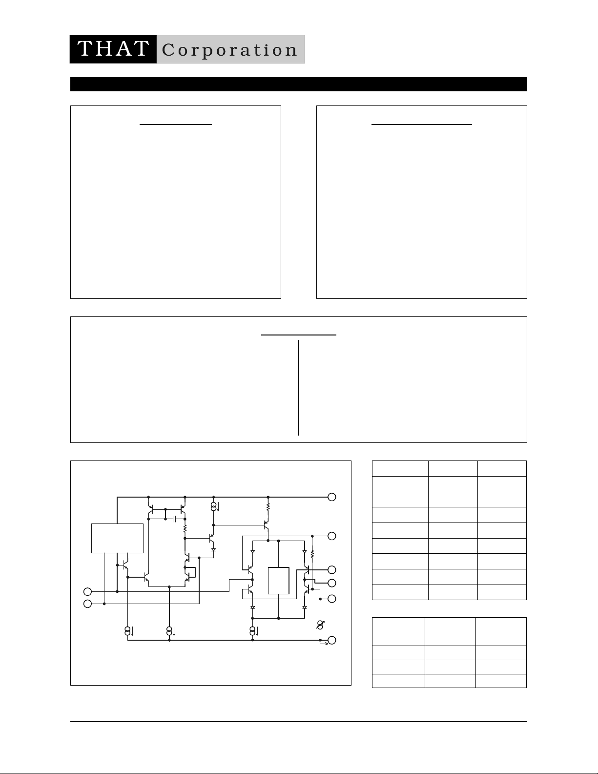
BIAS CURRENT
COMPENSATION
Input
1
6
Gnd
7
Iset
25
Output
Vcc
2
Ec+
Ec-
3
8
4
Sym
V-
5
Max Trimmed
@1V,1kHz,0dB
2k
Vbe
MULTI-
PLIER
Iadj
Figure 1. 2181 Series Equivalent Circuit Diagram
THAT Corporation; 45 Sumner Street; Milford, Massachusetts 01757-1656; US
Tel: +1 508 478 9200; Fax: +1 508 478 0990; Web: www.thatcorp.com
Copyright © 2008, THAT Corporation Document 600030 Rev 02
Table 1. Pin Assignments
THD
Table 2. Ordering information
Plastic
SIP
SO PinSIP PinPin Name
11Input
22Ec+
33Ec44Sym
55V66Gnd
77V+
88Output
Plastic
SO
2181AS08-U2181AL08-U0.01%
2181BS08-U2181BL08-U0.02%
2181CS08-U2181CL08-U0.05%
Page 2
Document 600030 Rev 02 Page 2 of 12 THAT 2181 Series
Blackmer® Trimmable IC VCAs
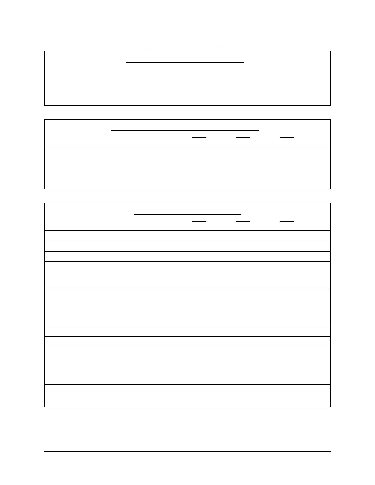
SPECIFICATIONS
Absolute Maximum Ratings
Positive Supply Voltage (VCC)+20 V
Negative Supply Voltage (V
Supply Current (I
Maximum ∆E
) 10 mA
CC
EC+ - (EC-) ± 1 V
C
) -20 V
EE
Power Dissipation (P
Operating Temperature Range (T
Storage Temperature Range (T
1
2,3
) (TA = 75 ºC) 330 mW
D
) 0 to +70 ºC
OP
) -40 to +125 ºC
ST
Recommended Operating Conditions
2181A 2181B 2181C
Parameter Symbol Conditions Min Typ Max Min Typ Max Min Typ Max Units
Positive Supply Voltage V
Negative Supply Voltage V
Bias Current I
Signal Current I
CC
EE
SET
+ I
IN
OUT
VCC - VEE = 30 V 1 2.4 3.5 1 2.4 3.5 1 2.4 3.5 mA
I
= 2.4 mA — 0.35 2.5 — 0.35 2.5 — 0.35 2.5 mA
SET
Electrical Characteristics
Parameter Symbol Conditions Min Typ Max Min Typ Max Min Typ Max Units
+4 +15 +18 +4 +15 +18 +4 +15 +18 V
-4 -15 -18 -4 -15 -18 -4 -15 -18 V
2
2181A 2181B 2181C
Supply Current I
Equiv. Input Bias Current I
Input Offset Voltage V
Output Offset Voltage V
CC
B
OFF(IN)
OFF(OUT)
No signal — 2.4 4 — 2.4 4 — 2.4 4 mA
No Signal — 2 10 — 2 12 — 2 15 nA
No Signal — ±5 — — ±5 — — ±5 — mV
R
= 20 kΩ
out
0 dB gain — 0.5 1 — 1 2 — 1.5 3 mV
+15 dB gain — 1 3 — 1.5 4 — 3 10 mV
+30 dB gain — 3 12 — 5 15 — 9 30 mV
Gain Cell Idling Current I
IDLE
Gain-Control Constant TA =25°C (T
CHIP
≅35°C)
—20 — —20 — —20 — µA
-60 dB < gain < +40 dB
/Gain (dB) Pin 2 (Fig. 15) 6.0 6.1 6.2 6.0 6.1 6.2 6.0 6.1 6.2 mV/dB
E
C+
/Gain (dB) Pin 3 -6.2 -6.1 -6.0 -6.2 -6.1 -6.0 -6.2 -6.1 -6.0 mV/dB
E
C-
Gain-Control TempCo ∆EC /∆T
CHIP
Ref T
= 27°C — +0.33 — — +0.33 — — +0.33 — %/°C
CHIP
Gain-Control Linearity -60 to +40 dB gain — 0.5 2 — 0.5 2 — 0.5 2 %
1 kHz Off Isolation EC+= -360mV,EC-=+360mV 110 115 — 110 115 — 110 115 — dB
Output Noise e
n(OUT)
20 Hz ~ 20 kHz
= 20kΩ
R
out
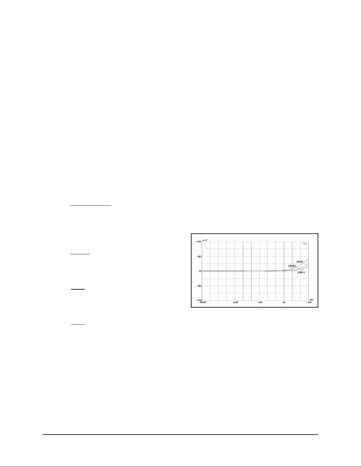
0 dB gain — -98 -97 — -98 -96 — -98 -95 dBV
+15 dB gain — -88 -86 — -88 -85 — -88 -84 dBV
Voltage at V- V
V-
No Signal -3.1 -2.85 -2.6 -3.1 -2.85 -2.6 -3.2 -2.85 -2.6 V
1. All specifications are subject to change without notice.
2. Unless otherwise noted, T
3. Stresses above those listed under “Absolute Maximum Ratings” may cause permanent damage to the device. These are stress ratings only; the functional operation of
the device at these or any other conditions above those indicated in the operational sections of this specification is not impli ed. Exposure to absolute maximum rating conditions for extended periods may affect device reliability.
=25ºC, VCC=+15V, VEE= -15V. Test circuit as shown in Figure 2. SYM ADJ is adjusted for minimum THD at 1 V, 1 kHz, Ec- = -Ec+ = 0 V.
A
THAT Corporation; 45 Sumner Street; Milford, Massachusetts 01757-1656; USA
Tel: +1 508 478 9200; Fax: +1 508 478 0990; Web: www.thatcorp.com
Copyright © 2008, THAT Corporation
Page 3
THAT 2181 Series Page 3 of 12 Document 600030 Rev 02
Blackmer® Trimmable IC VCAs
Electrical Characteristics (con’t)
2181A 2181B 2181C
Parameter Symbol Conditions Min Typ Max Min Typ Max Min Typ Max Units
Total Harmonic Distortion THD 1 kHz
V
= 0 dBV, 0 dB gain — 0.0025 0.005 — 0.004 0.008 — 0.005 0.02 %
IN
V
= +10 dBV, -15 dB gain — 0.018 0.025 — 0.025 0.035 — 0.035 0.07 %
IN
= -5 dBV, +15 dB gain — 0.018 0.025 — 0.025 0.035 — 0.035 0.07 %
V
IN
V
= +10 dBV, 0 dB gain — 0.004 0.008 — 0.006 0.010 — 0.015 — %
IN
Slew Rate RIN = R
Symmetry Control Voltage V
Gain at 0 V Control Voltage EC- = 0 mV -0.1 0.0 +0.1 -0.15 0.0 +0.15 -0.2 0.0 +0.2 dB
= 0dB, Minimum THD -0.5 — +0.5 -1.5 — +1.5 -2.5 — +2.5 mV
SYMAV
= 20 kΩ —12 — —12 — —12 —V/µs
OUT
2
Vcc
2181
Ec-
22p
Series
7
3
V+
-IN
V-
GND
5
EcEc+
6
1
SYM
2
4
OUT
8
20k
-
OP275
+
OUT
IN
10u
VCA
20k
Power Supplies
Vcc = +15 V
Vee = -15 V
5.1k
680k (2181A)
220k (2181B)
130k (2181C)
Vee
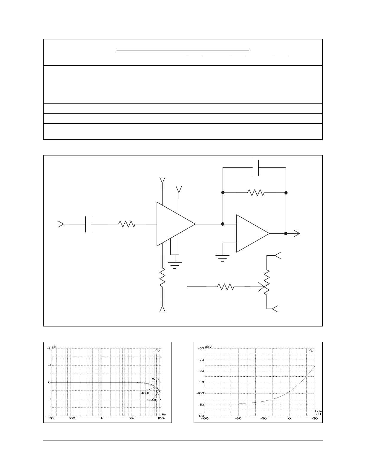
Figure 2. Typical Application Circuit
Rsym
50k
Vcc
SYM
ADJ
Vee
Figure 3. 2181 Series Frequency Response vs. Gain Figure 4. 2181 Series Noise (20kHz NBW) vs. Gain
THAT Corporation; 45 Sumner Street; Milford, Massachusetts 01757-1656; USA
Tel: +1 508 478 9200; Fax: +1 508 478 0990; Web: www.thatcorp.com
Copyright © 2008, THAT Corporation
Page 4
Document 600030 Rev 02 Page 4 of 12 THAT 2181 Series
A
A
.
Blackmer® Trimmable IC VCAs
Theory of Operation
The THAT 2181 Series VCAs are designed for
high performance in audio-frequency applications
requiring exponential gain control, low distortion,
wide dynamic range and low control-voltage
feedthrough. These parts control gain by converting
an input current signal to a bipolar logged voltage,
adding a dc control voltage, and re-converting the
summed voltage back to a current through a bipolar
antilog circuit.
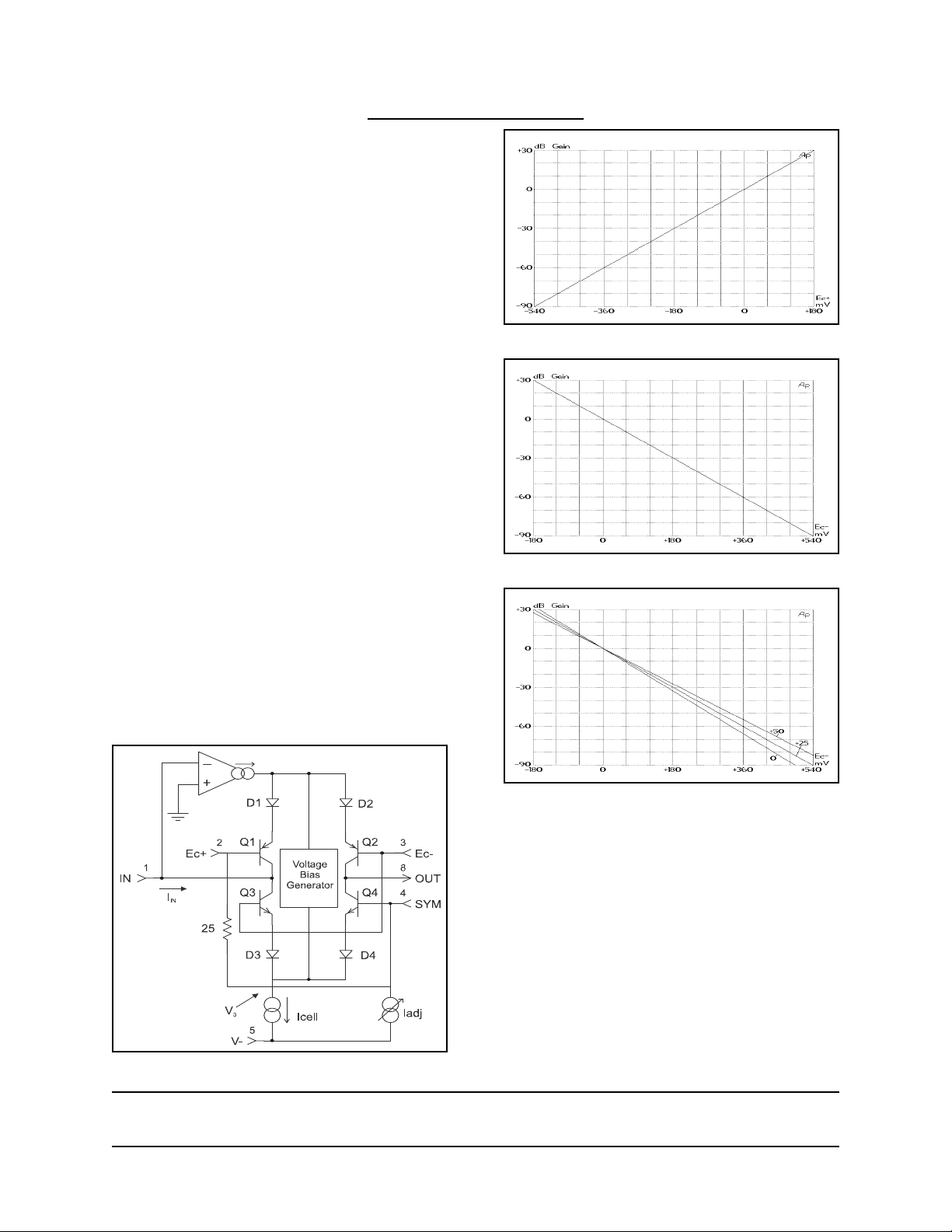
Figure 5 presents a considerably simplified internal circuit diagram of the IC. The ac input signal
current flows in pin 1, the input pin. An internal
operational transconductance amplifier (OTA) works
to maintain pin 1 at a virtual ground potential by
driving the emitters of Q1 and (through the Voltage
Bias Generator) Q3. Q3/D3 and Q1/D1 act to log the
input current, producing a voltage, V3, which represents the bipolar logarithm of the input current. (The
voltage at the junction of D1 and D2 is the same as
V3, but shifted by four forward V
Gain Control
Since pin 8, the output, is usually connected to a
virtual ground, Q2/D2 and Q4/D4 take the bipolar
antilog of V3, creating an output current which is a
precise replica of the input current. If pin 2 (E
pin 3 (E
connected to a high impedance current source), the
output current will equal the input current. For pin 2
positive or pin 3 negative, the output current will be
scaled larger than the input current. For pin 2
negative or pin 3 positive, the output current is
scaled smaller than the input.
) are held at ground (with pin 4 - SYM -
C-
drops.)
be
C+
) and
4
Figure 6. Gain vs. Control Voltage (EC+, Pin 2) at 25°C
Figure 7. Gain vs. Control Voltage (EC-, Pin 3) at 25°C
Figure 8. Gain vs. Control Voltage (E
) with Temp (°C)
C-
In normal operation, the output current is
converted to a voltage via an opamp-based I-V
converter, as shown in Figure 2, where the conversion ratio is determined by the feedback resistor
connected between the output and inverting input.
The signal path through the VCA and the output
opamp is non-inverting.
The scale factor between the output and input
currents is the gain of the VCA. Either pin 2 (Ec+) or
pin 3 (Ec-), or both, may be used to control gain.
Gain is exponentially proportional to the voltage at
pin 2, and exponentially proportional to the negative
of the voltage at pin 3. Therefore, pin 2 (Ec+) is the
Figure 5. Simplified Internal Circuit Diagram
4. For more details about the internal workings of the 2181 Series of VCAs, see An Improved Monolithic Voltage-Controlled
mplifier, by Gary K. Hebert (Chief Technology Officer, for THAT Corporation), presented at the 99th convention of the
udio Engineering Society, New York, Preprint number 4055
THAT Corporation; 45 Sumner Street; Milford, Massachusetts 01757-1656; USA
Tel: +1 508 478 9200; Fax: +1 508 478 0990; Web: www.thatcorp.com
Copyright © 2008, THAT Corporation
positive control port, while pin 3 (Ec-) is the
Page 5
THAT 2181 Series Page 5 of 12 Document 600030 Rev 02
Blackmer® Trimmable IC VCAs
negative control port. Because of the exponential
characteristic, the control voltage sets gain linearly
in decibels. Figure 6 shows the decibel current gain
of a 2181 versus the voltage at Ec+, while Figure 7
shows gain versus the Ec-.
Temperature Effects
The logging and antilogging in the VCA depends
on the logarithmic relationship between voltage and
current in a semiconductor junction (in particular,
between a transistor's V
this relationship is temperature dependent. Therefore, the gain of any log-antilog VCA depends on its
temperature.
Figure 8 shows the effect of temperature on the
negative control port. (The positive control port
behaves in the same manner.) Note that the gain at
Ec = 0 V is 0 dB, regardless of temperature. Changing temperature changes the scale factor of the gain
by 0.33%/°C, which pivots the curve about the 0 dB
point.
Mathematically, the 2181's gain characteristic is
Gain =
EC+− E
(0.0061)(1+0.0033 T)
where ∆T is the difference between room
temperature (25°C) and the actual temperature, and
Gain is the gain in decibels. At room temperature,
this reduces to
and IC). As is well known,
be
C−
, Eq. 1
Trimming
The 2181-Series VCAs are intended to be
adjusted for minimum distortion by applying a small
variable offset voltage to pin 4, the SYM pin. Note
that there is a 25 Ω resistor internal to the 2181
between pin 4 and pin 2. As shown in Figure 2,
Page 3, the usual method of applying this offset is to
use the internal 25 Ω resistor along with a larger
value resistor to form a voltage divider connected to
the wiper of a trim pot across the supply rails.
This trim should be adjusted for minimum
harmonic distortion. This is usually done by applying
a middle-level, middle-frequency signal (e.g. 1 kHz at
1 V) to the audio input, setting the VCA to 0 dB gain,
and adjusting the SYM trim while observing THD at
the output. In the 2181, this adjustment coincides
closely with the setting which produces minimum
control-voltage feedthrough, though the two settings
are not always identical.
DC Feedthrough
Normally, a small dc error term flows in pin 8
(the output). When the gain is changed, the dc term
changes. This control-voltage feedthrough is more
pronounced with gain; the –A version of the part
produces the least feedthrough, the –C version the
most. See Figure 9 for typical curves for dc offset vs.
gain
EC+− E
C−
Gain =
, Eq. 2
0.0061
If only the positive control port is used, this
becomes
E
C+
Gain =
, Eq. 3
0.0061
If only the negative control port is used, this
becomes
E
C−
Gain =
, Eq. 4
0.0061
DC Bias Currents
The 2181 current consumption is determined by
the resistor between pin 5 (V-) and the negative
supply voltage (V
resistor is 5.1 kΩ, which provides approximately
2.4 mA. This current is split into two paths: 570 μA
is used for biasing the IC, and the remainder
becomes I
CELL
er split in two parts: about 20 μA biases the core
transistors (Q1 through Q4), the rest is available for
input and output signal current.
). Typically, with 15V supplies, the
EE
as shown in Figure 5. I
CELL
is furth
Figure 9. Representative DC Offset vs. Gain
Audio Performance
The 2181-Series VCA design, fabrication and
testing ensure extremely good audio performance
when used as recommended. The 2181 maintains
low distortion over a wide range of gain, cut and
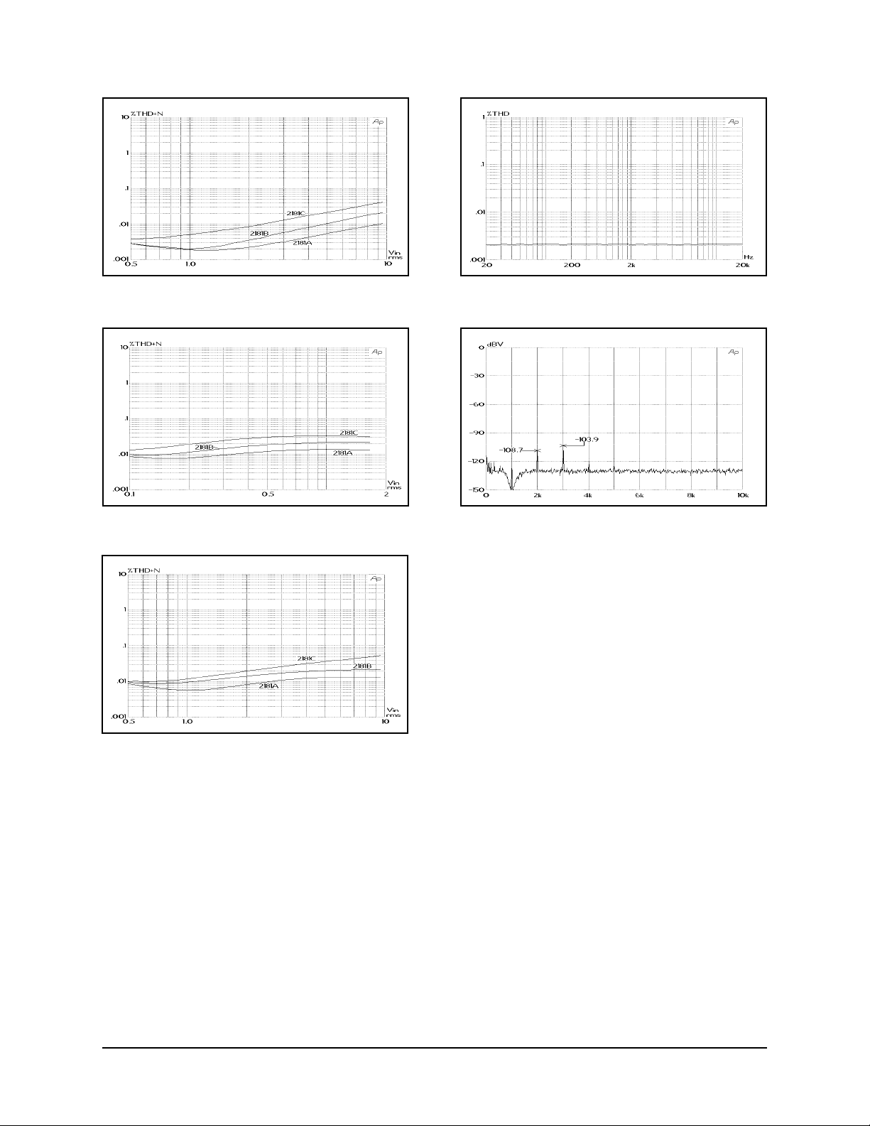
signal levels. Figures 10 through 12 show typical
distortion performance for representative samples of
each grade of the part. At or near unity gain, the
2181 behaves much like a good opamp, with low
distortion over the entire audio band. Figure 13
shows typical THD for a 2181A over frequency at 0
dB gain, with a 1 V input signal, while Figure 14
details the harmonic content of the distortion in a
typical A–grade part.
THAT Corporation; 45 Sumner Street; Milford, Massachusetts 01757-1656; USA
Tel: +1 508 478 9200; Fax: +1 508 478 0990; Web: www.thatcorp.com
Copyright © 2008, THAT Corporation
Page 6
Document 600030 Rev 02 Page 6 of 12 THAT 2181 Series
Blackmer® Trimmable IC VCAs
Figure 10. 1 kHz THD+Noise vs. Input Level, 0dB Gain
Figure 11. 1 kHz THD+Noise vs. Input Level, +15dB Gain
Figure 13. 2181A THD+N vs Frequency, 0dB gain 1kHz 1V
Figure 14. FFT of THD, Typical 2181A,
0dB Gain, 1V, 1kHz
Figure 12. 1 kHz THD+Noise vs. Input Level, -15dB Gain
THAT Corporation; 45 Sumner Street; Milford, Massachusetts 01757-1656; USA
Tel: +1 508 478 9200; Fax: +1 508 478 0990; Web: www.thatcorp.com
Copyright © 2008, THAT Corporation
Page 7

THAT 2181 Series Page 7 of 12 Document 600030 Rev 02
Blackmer® Trimmable IC VCAs
Applications
Input
As mentioned above, input and output signals are
currents, not voltages. While this often causes some
conceptual difficulty for designers first exposed to
this convention, the current input/output mode
provides great flexibility in application.
The Input pin (pin 1) is a virtual ground with
negative feedback provided internally (see Figure 5,
Page 4). The input resistor (shown as 20 kΩ in
Figure 2, Page 3) should be scaled to convert the
available ac input voltage to a current within the
linear range of the device. Generally, peak input
currents should be kept under 1 mA for best distortion performance.
Refer to Figures 10 through 12 to see how distortion varies with signal level for the three parts in the
2181 Series for 0 dB, +15 dB and -15 dB gain. The
circuit of Figure 2, Page 3 was used to generate these
curves.
For a specific application, the acceptable distortion will usually determine the maximum signal
current level which may be used. Note that, with
20 kΩ current-to-voltage converting resistors, distortion remains low even at 10 V rms input at 0 dB or
-15 dB gain, and at 1.7 V rms input at +15 dB gain
(~10 V rms output). This is especially true in the –A
and –B grades of the part.
Distortion vs. Noise
A designer may trade off noise for distortion by
decreasing the 20 kΩ current-to-voltage converting
resistors used at the input and output in Figure 2,
Page 3. For every dB these resistor values are
decreased, the voltage noise at the output of the
OP275 is reduced by one dB. For example, with
10 kΩ resistors, the output noise floor drops to
–104 dBV (typical) at 0 dB gain — a 6 dB reduction
in noise because 10 kΩ is 1/2 of (6 dB lower than)
20 kΩ.
Conversely, if THD is more important than noise
performance, increasing these resistors to 40 kΩ will
increase the noise level by 6 dB, while reducing
distortion at maximum voltage levels. Furthermore, if
maximum signal levels are higher (or lower) than the
traditional 10 V rms, these resistors should be
scaled to accommodate the actual voltages prevalent
in the circuit. Since the 2181 handles signals as
currents, these ICs can even operate with signal
levels far exceeding the 2181's supply rails, provided
appropriately large resistors are used.
High-Frequency Distortion
The choice of input resistor has an additional,
subtle effect on distortion. Since the feedback impedances around the internal opamp (essentially Q1/D1
and Q3/D3) are fixed, low values for the input resistor will require more closed-loop gain from the
opamp. Since the open-loop gain naturally falls off at
high frequencies, asking for too much gain will lead
to increased high-frequency distortion. For best
results, this resistor should be kept to 10 kΩ or
above.
Stability
An additional consideration is stability: the internal op amp is intended for operation with source
impedances of less than 60 kΩ at high frequencies.
For most audio applications, this will present no
problem.
DC Coupling
The quiescent dc voltage level at the input (the
input offset voltage) is approximately 0 V, but, as in
many general-purpose opamps, this is not well
controlled. Any dc input currents will cause dc in the
output which will be modulated by gain; this may
cause audible thumps. If the input is dc coupled, dc
input currents may be generated due to the input
offset voltage of the 2181 itself, or due to offsets in
stages preceeding the 2181. Therefore, capacitive
coupling is almost mandatory for quality audio applications. Choose a capacitor which will give acceptable low frequency performance for the application.
Summing Multiple Input Signals
Multiple signals may be summed via multiple
resistors, just as with an inverting opamp configuration. In such a case, a single coupling capacitor may
be located next to pin 1 rather than multiple capacitors at the driven ends of the summing resistors.
However, take care that the capacitor does not pick
up stray signals.
Output
The Output pin (pin 8) is intended to be
connected to a virtual ground node, so that current
flowing in it may be converted to a voltage (see
Figures 2 & 15). Choose the external opamp for good
audio performance. The feedback resistor should be
chosen based on the desired current-to-voltage
conversion constant. Since the input resistor determines the voltage-to-current conversion at the input,
THAT Corporation; 45 Sumner Street; Milford, Massachusetts 01757-1656; USA
Tel: +1 508 478 9200; Fax: +1 508 478 0990; Web: www.thatcorp.com
Copyright © 2008, THAT Corporation
Page 8

Document 600030 Rev 02 Page 8 of 12 THAT 2181 Series
Blackmer® Trimmable IC VCAs
the familiar ratio of Rf /Ri for an inverting opamp will
determine the overall voltage gain when the 2181 is
set for 0 dB current gain. Since the VCA performs
best at settings near unity gain, use the input and
feedback resistors to provide design-center gain or
loss, if necessary.
A small feedback capacitor around the output
opamp is needed to cancel the output capacitance of
the VCA. Without it, this capacitance will destabilize
most opamps. The capacitance at pin 8 is typically
15 pF.
Power Supplies
Positive
The positive supply is connected directly to V+
(pin 7). No special bypassing is necessary, but it is
good practice to include a small (~1 μf) electrolytic
or (~0.1 μf) ceramic capacitor close to the VCA IC on
the PCB. Performance is not particularly dependent
on supply voltage. The lowest permissible supply
voltage is determined by the sum of the input and
output currents plus I
through the output of the internal transconductance
amplifier and down through the core and voltage bias
generator. Reducing signal currents may help accommodate low supply voltages. THAT Corporation
intends to publish an application note covering
operation on low supply voltages. Please inquire for
its availability.
The highest permissible supply voltage is fixed by
the process characteristics and internal power
consumption. +18 V is the nominal limit.
Negative
The negative supply terminal is V- (pin 5). Unlike
normal negative supply pins, this point is intended to
be connected to a current source I
a resistor to V
able for the device. As mentioned before, this source
must supply the sum of the input and output signal
currents, plus the bias to run the rest) of the IC. The
minimum value for this current is 570 μA over the
sum of the required signal currents. Usually, I
should equal 2.4 mA for most pro audio applications
with ±15 V supplies. Higher bias levels are of limited
value, largely because the core transistors become
ineffective at logging and antilogging at currents over
1 mA.
), which determines the current avail-
EE
, which must be supplied
SET
(usually simply
SET
SET
Mathematically, this can be expressed as
≥ Peak (IIN) + Peak (I
I
CELL
I
= I
- 350 μA. Therefore,
SET
≥ Peak (IIN) + Peak (I
I
CELL
SET
) + 220 μA; and
OUT
) + 570 μA.
OUT
The voltage at V- (pin 5) is four diode drops
below ground, which, for the 2181, is approximately
-2.85 V. Since this pin connects to a (high
impedance) current supply, not a voltage supply,
bypassing at pin 5 is not normally necessary.
Ground
The GND pin (pin 6) is used as a ground reference for the VCA. The non-inverting input of the
internal opamp is connected here, as are various
portions of the internal bias network. It may not be
used as an additional input pin.
Voltage Control
Negative Sense
EC- (pin 3) is the negative voltage control port.
This point controls gain inversely with applied
voltage: positive voltage causes loss, negative voltage
causes gain. As described on Page 5, the current gain
of the VCA is unity when pin 3 is at 0 V with respect
to pin 2, and varies with voltage at approximately
-6.1 mV/dB, at room temperature.
Positive Sense
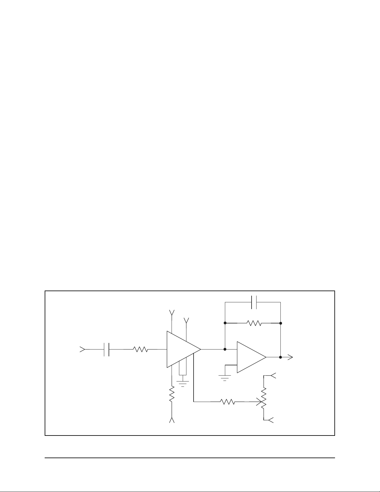
As mentioned earlier, EC+ (pin 2) is the positivesense voltage control port. A typical circuit using this
approach is shown in Figure 15. E
grounded, and E
(pin 2) driven from a
C+
low-impedance voltage source. Using the opposite
sense of control can sometimes save an inverter in
the control path.
Positive and Negative
It is also possible (and sometimes advantageous)
to drive both control ports, either with differential
drive (in which case, the control sensitivities of each
port are summed), or through two different control
signals. There is no reason why both control ports
cannot be used simultaneously.
(Pin 3) should be
C-
THAT Corporation; 45 Sumner Street; Milford, Massachusetts 01757-1656; USA
Tel: +1 508 478 9200; Fax: +1 508 478 0990; Web: www.thatcorp.com
Copyright © 2008, THAT Corporation
Page 9
g
THAT 2181 Series Page 9 of 12 Document 600030 Rev 02
Blackmer® Trimmable IC VCAs
Symmetry
The SYM pin (pin 4) is actually a sort of
additional positive-sense control port. It is provided
to allow V
adjusted after packaging and installation in the
circuit board. It should only be used for this
purpose. Connect pin 4 only to a high-impedance
source as shown in Figures 2 and 15.
mismatches in the core transistors to be
be
Control Port Drive Impedance
The control ports (pins 2 through 4) are
connected directly to the bases of the logging and/or
antilogging transistors. The accuracy of the logging
and antilogging is dependent on the E
voltages being exactly as desired to control gain. The
base current in the core transistors will follow the
collector currents, of course. Since the collector
currents are signal-related, the base currents are
therefore also signal-related. Should the source
impedance of the control voltage(s) be large, the
signal-related base currents will cause signal-related
voltages to appear at the control ports, which will
interfere with precise logging and antilogging, in turn
causing distortion.
The 2181 Series VCAs are designed to be
operated with zero source impedance at pins 2 and
3, and a high (≥50 kΩ) source impedance at pin 4.
To realize all the performance designed into a 2181,
keep the source impedance of the control voltage
driver well under 50 Ω.
This often suggests driving the control port
directly with an opamp. However, the closed-loop
and E
C+
output impedance of an opamp typically rises at hi
frequencies because open loop gain falls off as
frequency increases. A typical opamp's output impedance is therefore inductive at high frequencies.
Excessive inductance in the control port source
impedance can cause the VCA to oscillate internally.
In such cases, a 100 Ω resistor in series with a
1.5 nF capacitor from the control port to ground will
usually suffice to prevent the instability.
h
Noise Considerations
It is second nature among good audio designers
to consider the effects of noisy devices on the signal
path. As is well known, this includes not only active
C-
devices such as opamps and transistors, but extends
to the choice of impedance levels as well. High value
resistors have higher inherent thermal noise, and the
noise performance of an otherwise quiet circuit can
be easily spoiled by the wrong choice of impedance
levels.
Less well known, however, is the effect of noisy
circuitry and high impedance levels in the control
path of voltage-control circuitry. The 2181 Series
VCAs act like multipliers: when no signal is present
at the signal input, noise at the control input is
rejected. So, when measuring noise (in the absence
of signal – as most everyone does), even very noisy
control circuitry often goes unnoticed. However,
noise at the control port of these parts will cause
noise modulation of the signal. This can become
significant if care is not taken to drive the control
ports with quiet signals.
IN
Power Supplies
Vcc = +15 V
Vee = -15 V
THAT Corporation; 45 Sumner Street; Milford, Massachusetts 01757-1656; USA
Vcc
2181
Ec-
22p
Series
5.1k
1
7
V+
-IN
GND
V-
Vee
3
EcEc+
6
5
SYM
2
OUT
8
4
20k
-
OP275
+
Rsym
680k (2181A)
220k (2181B)
130k (2181C)
VCA
10u
Tel: +1 508 478 9200; Fax: +1 508 478 0990; Web: www.thatcorp.com
20k
Figure 15. Positive Control Port using Pin 4
Copyright © 2008, THAT Corporation
50k
OUT
Vcc
SYM
ADJ
Vee
Page 10

f
Document 600030 Rev 02 Page 10 of 12 THAT 2181 Series
Blackmer® Trimmable IC VCAs
The 2181 Series VCAs have a small amount o
inherent noise modulation because of its class AB
biasing scheme, where the shot noise in the core
transistors reaches a minimum with no signal, and
increases with the square root of the instantaneous
signal current. However, in an optimum circuit, the
noise floor rises only to -94 dBV with a 50 μA rms
signal at unity gain — 4 dB of noise modulation. By
contrast, if a unity-gain connected, non-inverting
5534 opamp is used to directly drive the control
port, the noise floor will rise to 92 dBV — 6 dB of
noise modulation.
To avoid excessive noise, one must take care to
use quiet electronics throughout the control-voltage
circuitry. One useful technique is to process control
voltages at a multiple of the eventual control constant
(e.g., 61 mV/dB — ten times higher than the VCA
requires), and then attenuate the control signal just
before the final drive amplifier. With careful attention
to impedance levels, relatively noisy opamps may be
used for all but the final stage.
Stray Signal Pickup
It is also common practice among audio designers to design circuit boards to minimize the pickup
of stray signals within the signal path. As with noise
in the control path, signal pickup in the control path
can adversely effect the performance of an otherwise
good VCA. Because it is a multiplier, the 2181
produces second harmonic distortion if the audio
signal itself is present at the control port. Only a
small voltage at the control port is required: as little
as 10 μV of signal can increase distortion to over
0.01%. This can frequently be seen at high frequencies, where capacitive coupling between the signal
and control paths can cause stray signal pickup.
Because the signal levels involved are very small,
this problem can be difficult to diagnose. One clue to
the presence of this problem is that the symmetry
null for minimum THD varies with frequency. It is
often possible to counteract a small amount of pure
fundamental picked up in the control path by
"misadjusting" the symmetry setting. Since the
amount of pickup usually varies with frequency, the
optimum trim setting will vary with frequency and
level. A useful technique to confirm this problem is
to temporarily bypass the control port to ground via
a modest-sized capacitor (e.g., 10 μF). If the distor-
tion diminishes, signal pickup in the control path is
the likely cause.
Temperature Sensitivity
As shown by Equation 1 (Page 5), the gain of a
2181 VCA is sensitive to temperature in proportion
to the amount of gain or loss commanded. The
constant of proportionality is 0.33% of the decibel
gain commanded, per degree Celsius, referenced to
27°>C (300°K). This means that at 0 dB gain, there
is no change in gain with temperature. However, at
-122 mV, the gain will be +20 dB at room temperature, but will be 20.66 dB at a temperature 10°C
lower.
For most audio applications, this change with
temperature is of little consequence. However, if
necessary, it may be compensated by a resistor
embedded in the control voltage path whose value
varies with temperature at the same rate of 0.33%/°C.
Such parts are available from RCD Components, Inc,
www.rcd-comp.com, and KOA/Speer Electronics,
www.koaspeer.com.
Closing Thoughts
THAT Corporation welcomes comments,
questions and suggestions regarding these devices,
their design and application. Our engineering staff
includes designers who have decades of experience in
applying our parts. Please feel free to contact us to
discuss your applications in detail.
THAT Corporation; 45 Sumner Street; Milford, Massachusetts 01757-1656; USA
Tel: +1 508 478 9200; Fax: +1 508 478 0990; Web: www.thatcorp.com
Copyright © 2008, THAT Corporation
Page 11
THAT 2181 Series Page 11 of 12 Document 600030 Rev 02
A
Blackmer® Trimmable IC VCAs
Package Information
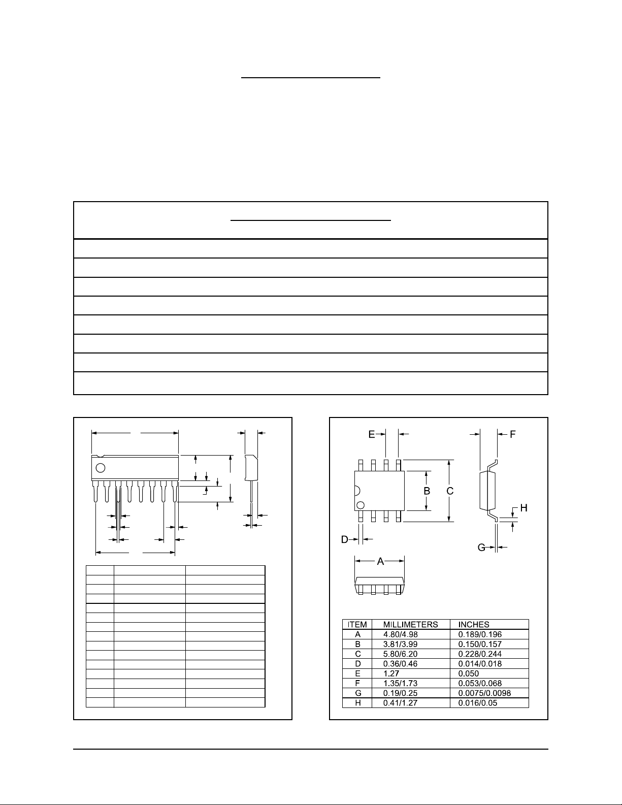
The THAT 2181-series is available in 8-pin SO and
8-pin SIP packages. Package dimensions are shown
in Figure 16 and 17 below; Pinouts are given in
Table 1 on page 1. Ordering information is provided
in Table 2 also on page 1.
The 2181-series packages are entirely lead-free.
The lead-frames are copper, plated with successive
layers of nickel, palladium, and gold. This approach
makes it possible to solder these devices using leadfree and lead-bearing solders.
Neither the lead-frame nor the plastic mold
compound used in the 2181-series contains any
hazardous substances as specified in the European
Union's Directive on the Restriction of the Use of
Certain Hazardous Substances in Electrical and
Electronic Equipment 2002/95/EG of January 27,
2003
Package Characteristics
Parameter Symbol Conditions Min Typ Max Units
Through-hole package See Figure 16 for dimensions 8 Pin SIP
Thermal Resistance θJA SIP package soldered to board 100 ºC/W
Environmental Regulation Compliance Complies with January 27, 2003 RoHS requirements
Surface-mount package See Figure 17 for dimensions 8 Pin SO
Thermal Resistance θJA SO package soldered to board 150 ºC/W
Soldering Reflow Profile JEDEC JESD22-A113-D (250ºC)
Moisture Sensitivity Level MSL Above-referenced JEDEC soldering profile 1
Environmental Regulation Compliance Complies with January 27, 2003 RoHS requirements
I
H
1
B
D
C
N
MILLIMETERS
ITEM
19.5 +0.2/-0
A
1.25
B
0.65
C
0.85
D
2.54 ±0.2
E
0.9
F
1.2
G
5.8 +0.2/-0
H
2.8 +0.1/-0
I
10.5 ±0.5
J
1.3
K
0.3
L
3.5 ±0.5
M
N 17.78 ±0.3 0.700 ±0.012
G
F
E TYP.
INCHES
0.77 +0.008/-0
0.049
0.026
0.033
0.100 ±0.008
0.04
0.05
0.23 +0.008/-0
0.11 +0.004/-0
0.413 ±0.02
0.05
0.012
0.14 ±0.02
J
M
K
L
Figure 16. -L (SIP) Version Package Outline Drawing Figure 17. -S (SO) Version Package Outline Drawing
THAT Corporation; 45 Sumner Street; Milford, Massachusetts 01757-1656; USA
Tel: +1 508 478 9200; Fax: +1 508 478 0990; Web: www.thatcorp.com
Copyright © 2008, THAT Corporation
Page 12

Document 600030 Rev 02 Page 12 of 12 THAT 2181 Series
Blackmer® Trimmable IC VCAs
Notes
THAT Corporation; 45 Sumner Street; Milford, Massachusetts 01757-1656; USA
Tel: +1 508 478 9200; Fax: +1 508 478 0990; Web: www.thatcorp.com
Copyright © 2008, THAT Corporation
 Loading...