

THAT Corporation
IC Voltage-Controlled
Amplifiers
THAT 2151, 2150A, 2155
FEATURES
• Wide Dynamic Range: >116 dB
• Wide Gain Range: >130 dB
• Expo nential (dB) Gai n Control
• Low Distortion: (0.008% @ 0 dB
gain, 0.035% @15dB gain)
• Wide Gain-Bandwidth: 6 MHz
• Low Cost: $2.20 in ’000s (2155)
• Single In-L ine Packa ge
• Dual Gain-Control Ports (pos/neg)
Description
The THAT 2150 Series integra te d -c ircuit volt age controlled amplifiers (VCAs) are high-performance
current-in/current-out devices with two opposingpolarity, voltage-sensitive control ports. Based on
dbx technology, they offer wide-range exponential
control of gain and attenuation with low signal distortion . The pa rts are h oused in a sp ace-efficient,
plastic 8-pin single-in-line (SIP) package, and re-
APPLICATIONS
• Faders
• Panners
• Compressors
• Expanders
• Equalizers
• Filters
• Oscillators
• Automation Systems
quire minimal support circuitry. Fabricated in a
super low-nois e process utilizing high hFE, complementary NPN/PNP pairs, the 2150 Series VCAs
combine high gain-bandwidth product with low
noise, low distortio n, and l ow offse t to offer d i s cr e te
performance at IC prices. They are available in
three grades, selected for distortion, allowing the
user to optimize cost vs. performance.
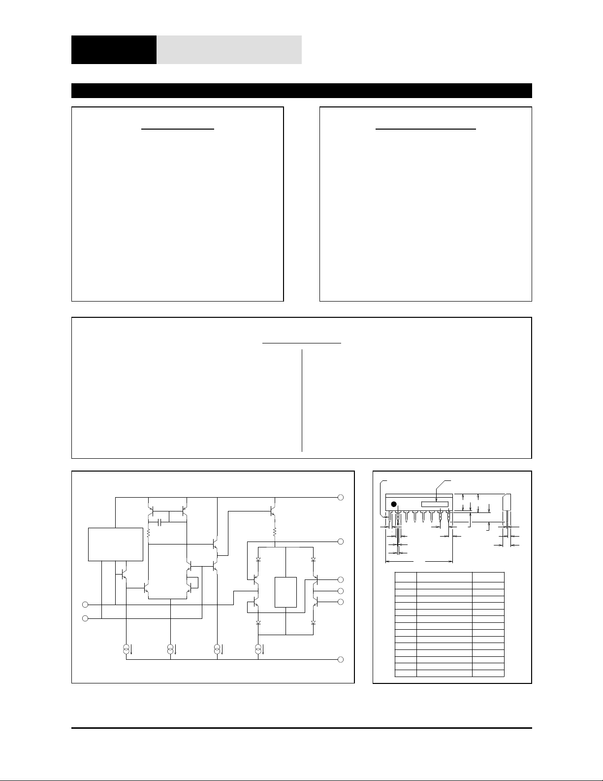
BIAS CURRENT
COMPENSATION
1
6
Vbe
MULTI-
PLIER
Figure 1. 215 0 S e rie s Equi v a le n t Circuit Diagr am
dbx is a registered trademark of Ca r illon Electronics Co r p ora tion
THAT Corporation; 734 Fo rest Street; Marlborou g h , Mas sach usetts 01752; USA
Tel: (508) 229-2500; Fax: (508) 229-2590; Web: http://www.thatcorp.com
PIN 1
7
2
THAT
N
TYP.
B
D
C
MODEL NO.
H
J
GE
M
F
L
K
I
A
3
8
4
5
ITEM MILLIMETERS INCHES
A 20.32 MAX.
B
1.1 MIN.
+_
.1
C
0.5
0.25
D
2.54
E
F
1.27 MAX.
G
0.51 MIN.
H
5.08 MAX.
+
_
.2
2.8
I
5.75 MAX.
J
1.5 MAX.
K
L
MN3.2
0.25
1.1 MIN.
_
+.10
.04
+
_
.5
0.8 MAX.
0.043 MIN.
_
+
0.02
0.01
0.1
0.05 MAX.
0.02 MIN.
0.2 MAX.
+
_
.008
0.11
0.227 MAX.
0.058 MAX.
.004 .002+
0.01
0.126
0.043 MIN.
.004
+
_
_
.02
Figure 2. 2150 Series Physical Outline
Page 2 2150 Series IC VCAs
SPECI FICATIONS
1
Absolute-Maximum Ratings (TA = 25˚C)
Positive Supply Voltage (VCC) +18 V
Negative Supply Voltage (VEE) -18 V
Supply Current (ICC)10 mA
Power Dissipation (PD) (TA = 75˚C) 330 mW
Operating Temperature Range (TOP) -20 to +75˚C
Storage Tempe rat ur e R an g e ( TST) -40 to +125˚C
Recommended Operating Conditions
2151 2150A 2155
Parameter Symbol Conditions Min Typ Max Min Typ Max Min Typ Max Units
Positive Supply Voltage V
Negative Supply Voltage V
Bias Current I
Signal Current I
IN+IOUT
SET
CC
EE
VCC-VEE= 24 V — 2.4 4 — 2.4 4 — 2.4 4 mA
I
= 2.4 mA — 175 750 — 175 750 — 125 550 µArms
SET
Electrical Characteristics
+5 +12 +15 +5 +12 +15 +5 +12 +15 V
-5 -12 -15 -5 -12 -15 -5 -12 -15 V
2
2151 2150A 2155
Parameter Symbol Conditions Min Typ Max Min Typ Max Min Typ Max Units
Supply Current I
Equiv. Input Bias Current I
Input Offset Voltage V
Output Offset Voltage V
Gain Cell Idling Current I
Gain-Control Constant T
Gain-co nt rol Temp Co ∆ EC / ∆ T
Gain-Control Linearity -60 to +40 dB gain — 0.5 2 — 0.5 2 — 0.5 2 %
Off Isolation (Fig. 14) EC+=-360mV, EC-=+360mV 110 115 — 110 115 110 115 — dB
Output Noise e
CC
B
OFF(IN)
OFF(OUT)
IDLE
/Gain (dB) Pins 2 & 4 (Fig. 14) 6.0 6.1 6.2 6.0 6.1 6.2 6.0 6.1 6.2 mV/dB
E
C+
EC-/Gain (dB) Pin 3 -6.0 -6.1 -6.2 -6.0 -6.1 -6.2 -6.0 -6.1 -6.2 mV/dB
CHIP
n(OUT)
No Signal — 2.4 4 — 2.4 4 — 2.4 4 mA
No Signal — 5 8 — 5 8 — 5 8 nA
No Signal — +10 — — +10 — — +10 — mV
R
=20 kΩ
out
0 dB gain — 1 3 — 1 3 — 1 3 mV
+15 dB gain — 2 3 — 2 3 — 2 3 mV
+40 dB gain — 5 15 — 7 15 — 10 15 mV
—20— —20— —20— µA
=25˚C (T
A
-60 dB < gain < +40 dB
Ref T
20 Hz-20 kHz
R
+15 dB gain — -88 -86 — -88 -86 — -88 -86 dBV
≅35˚C)
CHIP
= 27˚C — +0.33 — — +0.33 — — +0.33 — %/˚C
CHIP
= 20kΩ
out
0 dB gain — -98 -97 — -98 -96 — -98 -96 dBV
1. All specifications subject to change without notice.
2. Unless otherwise noted, TA=25˚C, VCC = +15V, VEE= -15V. Test circuit is as shown in Figure 3. SYM
justed for minimum THD @ Vin=1 V, 1 kHz, 0 dB gain.
THAT Corporation; 734 Fo rest Street; Marlborou g h , Mas sach usetts 01752; USA
Tel: (508) 229-2500; Fax: (508) 229-2590; Web: http://www.thatcorp.com
ADJ
is ad-
Rev. 10/25/96 Page 3
Electrical Characteristics (Cont’d.)
2151 2150A 2155
Parameter Symbol Conditions Min Typ Max Min Typ Max Min Typ Max Units
Total Harmonic Distortion THD IIN+ I
= 180 µA, 1 kHz
OUT
0 dB gain — 0.004 0.02 — 0.005 0.03 — — — %
±15 dB gain — 0.025 0.045 — 0.05 0.07 — — — %
+ I
= 150 µA, 1 kHz
I
IN
OUT
0 dB gain — — — — — — — 0.006 0.03 %
±15 dB gain — — — — — — — 0.05 0.07 %
Symmetry Control Voltage V
Gain at 0 V Control Voltage E
AV= 0 dB, THD < 0.07% -1.6 0 +1.6 -2 0 +2 -2.5 0 +2.5 mV
SYM
INPUT
10u
= 0 mV -0.1 0.0 +0.1 -0.15 0.0 +0.15 -0.2 0.0 +0.2 dB
C–
+15V
-
LF351
+
47p
20k
OUTPUT
20k
Ec-
2150
GND
Series
VCA
3
Ec-
OUT
Ec+
Ec+
6
8
4
2
7
V+
1
-IN
V-
5
+15V
5.1k
51
Rsym
150k
300k (2155)
390k (2150A)
470k (2151)
50k
SYM
ADJ
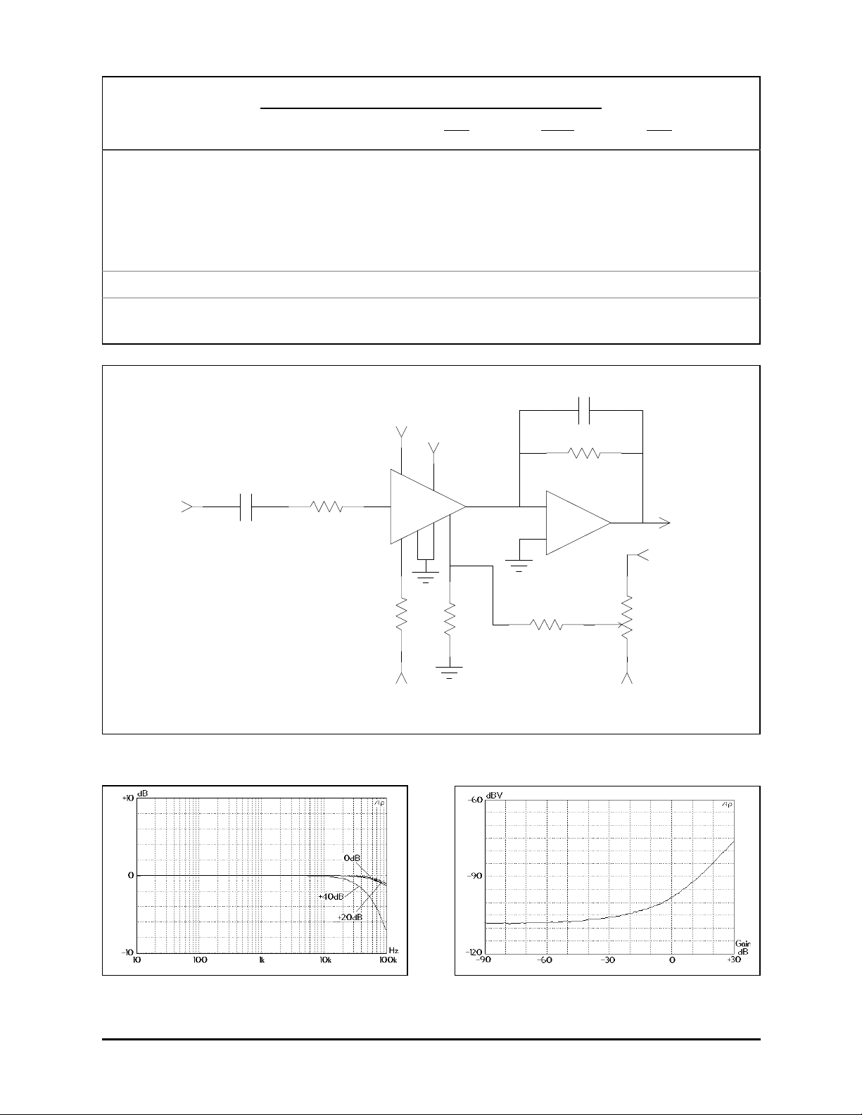
Figure 3. Typical Application Circuit
Figure 4. Frequency Response Vs. Gain (2150A)
THAT Corporation; 734 Fo rest Street; Marlborou g h , Mas sach usetts 01752; USA
Tel: (508) 229-2500; Fax: (508) 229-2590; Web: http://www.thatcorp.com
-15V-15V
Figure 5. Noise (20kHz NBW) Vs. Gain (2150A)

Page 4 2150 Series IC VCAs
Theory of Operation
The THAT 2150 Series VCAs are designed for high
performance in audio-frequency applications requiring
exponential gain control, low distortion, wide dynamic
range an d low dc bias modulat ion. These parts contr ol
gain by converting an input current signal to a bipolar
logged voltage, adding a dc control voltage, and re-co nverting the su mmed vol tage back to a current through
a bipolar antilog circuit.
Figure 6 presents a cons iderably simplif ied internal
circuit diagram of the IC. The ac input signal current
flows in pin 1, the input pin. The internal op amp
works to maintain pin 1 at a virtual ground potential
by driving the emitters of Q1 and (through the Voltage
Bias Generator) Q3. For positive input currents (Iin de-
fined as flowing into pin 1), the op amp drives the emitter of Q1 negative, turning off its collector current,
while simultaneously driving the emitter of Q3 nega-
-
+
D1
Q1
2
Ec+
1
IN
Ii
n
V
V-
Voltage
Bias
Generator
D3
3
5
D2
Q2
Q4Q3
D4
3
Ec-
8
OUT
4
Ec+
(SYM)
Figure 6. Simpl ified I nternal Cir c uit Diag ram
tive, turni ng it on. T he input s ignal c urrent, the refore,
is forced to flow through Q3 and D3.
Logging & Antilogging
Because the voltage across a base-emitter junction
is logarithmic with collector current, the voltage from
the base of Q3 to the cathode of D3 is proportional to
the log of the positive input current. The voltage at the
cathodes of D3 and D4 is therefore proportional to the
log of the positive input currents plus the voltage at
pin 3, the negative control port. Mathematically,
I
V3 = EC− − 2VT ln
where V3 is the voltage at the junct ion of D3 and D4;
C3
,
I
S
VT is the therma l volt age,
kT
; IC3 is the collect or cur-
q
ren t of Q 3; and IS is the r everse- saturation curr ent of
Q3. It is assumed that D3 matches Q3 (and will be assumed that they match Q4 and D4, as well).
In typical applications (see Figure 3, Page 3), pin 4
is connected to a voltage source at ground or nearly
ground potential. Pin 8 is connected to a virtual
ground (usually the inverting input of an op amp with
negative fe edback around it). With p in 4 near ground,
and pin 8 at virtual ground, the v olta g e a t t h e ca th o de s
of D3 and D4 will cause an exponentially-related current to flow in D4 and Q4, and out via pin 8. A similar
equation governs this behavior:
I
V3 = EC+ − 2VT ln
C4
.
I
S
Exponential G ain Contr ol
The similarity between the two preceeding equations
begs further exploration. Accordingly:
I
V3 = EC+ − 2VT ln
EC+ − EC− = 2VT ln
= 2VT ln
C4
= EC− − 2VT ln
I
S
I
C4
− 2VT ln
I
S
I
C4
.
I
C3
Rearranging terms,
EC+−E
C−
IC4 = IC3 e
2V
.
T
If pin 3 and pin 4 are at ground potential, the current in Q4/D4 will precisely mirror that in Q3/D3.
When pin 3 is positive with respect to pin 4, the voltage
across t he base-emitter junction of Q3 is higher than
that across the base-emitter junction of Q4, so the
Q4/D4 current remains proportional to, but less than,
the c urrent in Q3/D3. In th e same manner, a n eg ative
voltage at pin 3 with respect to pin 4 causes the
Q4/D 4 curren t to be pr oportio nal to, b ut great er than
that in Q3/D3.
The ratio of currents is exponential with the difference in the v ol tag es EC+ and EC–, providing convenient
“deci-linear” control. Mathematically, this is:
EC+−E
AV =
I
C4
= e
I
C3
C−
2V
, where AV is the current gain.
T
For pi n 4 a t or ver y near gr ound, at r oom temper ature (25˚C), allowing for a 10˚C internal temperature
rise, and converting to a base of 10 for the exponen t i al,
this redu c es to:
I
C3
I
S
I
C3
I
S
THAT Corporation; 734 Fo rest Street; Marlborou g h , Mas sach usetts 01752; USA
Tel: (508) 229-2500; Fax: (508) 229-2590; Web: http://www.thatcorp.com

Rev. 10/25/96 Page 5
−E
C−
0.122
AV = 10
.
When pin 3 is at O V, the current ratio is unity.
When pin 3 is at +122 mV, the output current (Q4) is
10 times (20 dB) less than the input current. At
–122 mV, the output current is 10 times (20 dB)
greater than the input current. Another way of expressing this relationship is:
−E
Gain =
C−
, where Gain is the gain in decibels.
0.0061
Negative I npu t Cu rrents
For negative input currents, Q1/D1 operate with
Q2/D2 to mirror the lower -half-core behavior. Pin 2 is
normally at or v ery near ground (see the section below
on Symmetr y Adju stment fo r more detail), so the same
gain s cal in g ap pli ed to t he base o f Q3 is a ppl ied to th e
base of Q2. The polarity (positive/negative, in dB) of
the gain is the same for the top pair versus the bottom
Transistor M a tching
The bias current flows downwards in the core (from
Q1 to Q3, and from Q2 to Q4) so long as there is good
matching betwee n all four compound transistors (transistors plus diodes). Mismatches will caus e a dc output
current to flow in pin 8, which will ultimately manifest
itself as a dc offset voltage. Static offsets are of little
consequence in most audio applications, but any mismatch-caused dc output current will be modulated by
gain commands, and may become audibl e as “thump s”
if lar ge, f as t gai n ch ang es a re comm anded in the pre sence of significant mismatches.
Transistor matching also affects distortion. If the
top half of the gain cell is perfectly matched, while the
bottom half is slightly off, then the gain commanded by
the voltage at pin 3 will affect the two halves of the core
differently. Since positive and negative halves of ac
input signals are handled by separate parts of the core,
this gives rise to even-order distortion products.
pair of the four “core” transistors because their sexes
(NPN/PNP) are inverted in the top versus the bottom,
while the ba ses are cross -conne cted between the input
(left) half and the output (right) half of each pair.
The resulting control over gain is extremely consistent from unit to unit, since it derives from the physics
of semicond uctors. Figure 7 shows actual dat a from a
typical 2150 Series VCA, taken at 25˚C.
Symmetry Adjustment
The monolithic construction of the devices assures
relatively good matching between the paired transistors, but even small VBE mismat ches can c ause unacceptable asymmetries in the output. For this reason,
the bases of Q1 and Q4 are brought out separately to
pin 2 and pin 4, respectively. This allows a small s tatic
voltage differential to be applied to the two bases. The
applie d voltage m ust be set to equal the sum of the V
mismatches ar ound the core (which varies from sample
to sample ). Figure 3 (Page 3) includes a typical circuit
to appl y thi s sy mmetry voltage. R
controls primarily
SYM
even-order harmonic distortion, and is usually adjusted for minimum THD at the output . Figure 8 plots
THD vs. the voltage between pins 2 and 4 (the two E
ports) for various gain settings of a typical part.
BE
C+
Figure 7. Gain Versus Control Voltage (Pin 3) at 25˚C
Core Bias Currents
A quiescent bias current in the core transistors is
established by the Voltage Bias Generator shown in
Figure 6. This current acts like crossover bias in the
output stag e of a complementary cl ass AB power amplifier, smoothing the transition between turning on
the top (PNP) pair and th e bott om (NPN) pair o f trans istors in the core. This lowers distortion greatly at some
cost to noise performance, as the current noise of the
core transistors (wh ich run at approximately 20 µA) is
the dominant noise source in the 2150 Series VCAs.
THAT Corporation; 734 Fo rest Street; Marlborou g h , Mas sach usetts 01752; USA
Tel: (508) 229-2500; Fax: (508) 229-2590; Web: http://www.thatcorp.com
Opposite Pol a rity Control
As may be se en fro m th e m ath ema ti cs , the bases o f
Q1 and Q4 can al so be used as an addit ional control
Figure 8. Typical THD Versus Symmetry Voltage

Page 6 2150 Series IC VCAs
port, with an opposite sense of control from that at
pin 3. To use this port, both pins must be driven with
the control voltage, while a small differential voltage is
accommodated between the two pins. (Figure 14,
Page 9, shows the typical connection.) Either pin 3, or
pins 2 and 4, or both ports together may be used for
gain control. Mathematically, this relationship is as follows:
EC+−E
C−
AV = 10
Gain =
0.122
Ec+ − E
0.0061
, where AV is the gain in volts/volt, or
c−
, where Gain is the gain in decibels.
Control Port Source Impedance
The control ports (pins 2 through 4) are connected
directly to the bases of the logging and/or antilogging
transistors. As was implied in the earlier discussion on
Loggin g and Antilogging (Page 4) the accuracy of the
logging and an tiloggin g is dependent on the EC+ and
EC- voltages being exactly as desired to control gain.
The base current in the transistors will follow the collector currents, of course. Since the collector currents
are signal-related, the base currents will also be signalrelated. Should the source impedance of the control
voltage(s) be large, the signal-related base currents will
cause signal-related voltages to appear at the control
ports, which will interfere with precise logging and
antilogging, in turn causing distortion.
The 2150 Series VCAs are designed to be operated
with zero source impedance at pins 2 and 3, and a 50Ω
source impedance at pin 4. (Pin 4 is intende d for connection to the symmetry control, hence the higher design-center source impedance.) One can estimate the
distortion caused by a spe cifi c, non -zero so urc e imp e dance by determ ining the base voltage modulation due
to signal current based on a core-transistor β of approximately 300 (NPN) or 100 (PN P), a nd converting the
resulting decibel gain modulation to a percentage.
Even 100Ω can spoil the good performance of these
parts at high signal levels.
DC Input Signals
Any dc currents in the feedback loop of the internal
op amp will s how up as dc ter ms in the output signal,
and will be modulated by gain commands. Input bias
currents will cause a dc current to flow in the feedback
loop provided by the input side of the core. For this
reason, input bias currents in the internal op amp
must be kept very low. The bias current compensation
at the input stage provides excellent cancellation of the
bias current required by the input differential amplifier. Of course, this good performance can be negated
by a dc current supplied from outsid e the VCA. To pre -
vent such dc ter ms, ac i nput coupling is strongly recommended. A plot of typical output offset voltage versus gain for the circuit of Figure 3 is shown in
Figure 9. (T he LF351’s offset was adjusted to 0 V for
this plot.)
Figure 9. DC Offs e t V s. Ga in , Af te r S ym me t ry
Adjustment
Current Programming
The size of the current source at the bottom of the
core (Figure 6, Page 4) is programm ed exter nally via
I
, which is normally determined by a resistor from
SET
pin 5 to V–. The voltage at pin 5 is typically –2.7 V. I
SET
divides into t wo po rti ons: a pproximately 4 00 µA is used
for internal biasing, and the rest is available for the
current source at the bottom of the core. I
SET
should
the refor e be 40 0 µA larger than the total of the peak
input and output signal currents.
Note that the output impedance of the internal opamp is approximately 2 kΩ, and un der pea k demands,
the sum of the input and output currents plus I
SET
must be supplied through this impedance, lowering the
voltage available to drive the core. For more information, see th e Power Supplies section on Page 8.
Headroom
Maximum signal currents are also limited by the
logarithmic characteristics of the core transistors. In
the 2150 Series, these devices are specially constructed to conform to an ideal log-linear curve over a
wide range of currents, but they reach their limit at approximately 1 mA. The symptom of failing log conformance is increasing distortion with increasing current
levels. The onset of distortion is gradual at low current
levels, and then more rapid as current becomes high.
Figures 10 through 12 show distortion versus signal
leve l f or th e t hre e pa rts in th e 21 50 Seri es fo r -15 dB,
0 dB, and +15 dB gain. The acceptable distortion will
determine the maximum signal level for a particular
design.
THAT Corporation; 734 Fo rest Street; Marlborou g h , Mas sach usetts 01752; USA
Tel: (508) 229-2500; Fax: (508) 229-2590; Web: http://www.thatcorp.com

Rev. 10/25/96 Page 7
Figure 10. 1kHz THD+Noise Vs. Input, -15 dB Gain
Figure 12 . 1k Hz TH D+ N oi s e Vs. Input, +15 dB Ga in
Applications
Input
As mentioned above, input and output signals are
currents, not voltages. While this often causes some
conceptual difficulty for designers first exposed to this
convention, the current input/output mode provides
great flexibility in application.
The input pin (pin 1) is a virtual ground with negative feedback provided internally (see Figure 6, Page 4).
The input resistor (shown as 20 kΩ in Figure 3, Page 3)
should be scaled to convert the available ac input voltage to a current within the linear range of the device.
(Peak input currents should be kept under 1 mA for
best distortion performance.) An additional consideration is stability: the internal op amp is intended for
operation with source impedances of less than 30 kΩ
at high frequencies. For most audio applications, this
will present no problem.
Figure 11. 1kHz THD+Noise Vs. Level, 0 dB Gain
the open-loop gain naturally falls off at high frequencies, asking for too much gain will lead to increased
high-frequency distortion. For best results, this resistor should be kept to 10 kΩ or above. Distortion vs. frequency for a 1 V signal at 0 dB gain with a 20 kΩ input
resistor is plotted in Figure 13.
The quiescent dc voltage level at the input is approximately +10 mV. As mentioned above, any dc input
currents will cause dc signals in the output which will
be modulated by gain, causing audible thump. There-
The ch oice of inp ut resist or has an add itional, subtle effect on distortio n. Since the feedback impedances
around the internal opamp (essentially Q1/D1 and
Q3/D3) are fixed, low values for the input resistor will
require more closed-loop gain from the opamp. Since
THAT Corporation; 734 Fo rest Street; Marlborou g h , Mas sach usetts 01752; USA
Tel: (508) 229-2500; Fax: (508) 229-2590; Web: http://www.thatcorp.com
Figure 13. THD Vs. Frequency, 0 dB Gain

Page 8 2150 Series IC VCAs
fore, capacitive coupling is almost mandatory for quality audio applic ations. Choose a capacitor which will
give ac ceptable l ow frequency p erformanc e for the application.
Multiple signals may be summed by multiple resistors, just as with an inverting op amp configuration. In
such a case, a single coupling capacitor may be lo cat ed
next to pin 1 rather than multiple capacitors at the
driven ends of the summing resistors. However, take
care that the capacitor does not act as an antenna for
stray signals.
Output
The output pin (pin 8) is int ended to be conne c te d to
a virtual ground node, so that current flowing in it ma y
be converted to a voltage (see Figures 3, 14, & 15).
Choose the external op amp for good audio performanc e. Th e fee dbac k resist or shou ld be ch osen base d
on th e desire d current-t o-voltag e convers ion consta nt.
Since the input resistor determines the voltage-to-current conversion at the input, the familiar ratio of Rf/R
for an inverting op amp will determine the overall voltage gain when t he VCA IC is set for 0 dB current gain.
Since the VCA performs best at settings near unity
gain, use the input and feedback resistors to provide
design-center gain or loss, if necessary.
A small feedback capacitor around the output op
amp is necessary to cancel the output capacitance of
the VCA. Without it, this capacitance will destabilize
most op amps. The capacitance at pin 8 is typically
30 pf.
Power Supplies
The positiv e supply is connected directly to pin 7.
No special bypa ssing is neces sary, b ut it is good practice to include a small (~1 µf) electrolytic close to the
VCA IC on the PCB. Performance is not particularly dependent on supply voltage. The lowest permissible supply voltage is determined by the sum of the input and
output currents plus I
through the resistor at the top of the core transistors
(see Figure 1 ) while s t ill allowing enough voltage swing
to bias the internal op amp and the core transistors
themselves. This resistor is approximately 2 kΩ. Reducing signal currents may help accommodate low
supply voltages.
The highest permissible supply voltage is fixed by
the process characteristics and internal power consumption. +15 V is the nominal limit.
The negative supply ter minal is intended to be connected to a resistive current source, which determines
the current available for the core. As mentioned before,
, which must be supplied
SET
this source must supply the sum of the input and output signal currents, plus the bias to run the rest of the
IC. The min imu m val ue f or th is curr ent i s 430 µA over
the sum of the required signal currents. 2.4 mA is recommended for most pro audio applications where
+15 V sup plies are common and headr oom is important.
Higher bias levels are of limited value, partly because the resistor mentioned in the positive su pply discussion must supply all the current devoted to the
core, and partly because the core transistors become
ineffective at logging and antiloggi ng at currents over
1 mA.
Since pin 5 is intended as a current supply, not a
voltage supply, bypassing at pin 5 is not necessary.
Pin 6 is used as a ground reference for the VCA. The
non-inverting input of the internal op amp is connected here, as are various portions of the internal bias
network. It may not be used as an additional input pin.
i
Voltage Control
The primary v oltage-control pin is pin 3. This point
controls gain inversely with applied voltage: positive
voltage caus es loss, negative v oltage causes gain. As
described on Page 6, the current gain of the VCA is
unity when pin 3 is at 0 V with respect to pins 2 and 4,
and va ries wi th voltag e at approxima tely -6.1 mV/dB,
at room temperature.
As implied by the equation for AV (at the foot of
Page 4), the gain is sensitive to temperature, in proportion to the amount of gain or loss commanded. The
constant of proportionality is 0.33% of the decibel gain
commanded, per degree Celsius, referenced to 27°C
(300°K). This means that at 0 dB gain, there is no
change i n ga i n wit h temperat ure. Ho we ver, at -122 mV,
the gain will be +20 dB at room temperature, but will
be 20.66 dB at a temperature 10˚C lower. The formula
is:
EC+−E
Gain =
(0. 0061 ) (1+ 0. 00 33 ) ∆T
where EC is in volts, and ∆T is the difference between
the actual temperature and room temperature (25˚C).
For most audio ap plications, thi s change with temperature is of little consequence. However, if necessary,
it may be compensated by a resistor which varies its
value by .33%/˚C. Such parts are available from RCD
Components, Inc, 3301 Bedford St., Manchester, NH,
USA [(603) 669-0054], and KOA/Speer Electronics, PO
Box 547, Bradford, PA, 16701 USA [(814)362-5536].
When pin 3 is used for voltage control, pin 2 is connected to ground and pin 4 is used to apply a small
C−
,
THAT Corporation; 734 Fo rest Street; Marlborou g h , Mas sach usetts 01752; USA
Tel: (508) 229-2500; Fax: (508) 229-2590; Web: http://www.thatcorp.com

Rev. 10/25/96 Page 9
symmetry voltage (<±2.5 mV) to co rrect for VBE mismatches within the VCA IC. For this purpose, the 2150
series devices were designed for optimum performance
with an impedance of approximately 50Ω at pin 4. A
trim pot is used to adjust the voltage between pin 4
and pin 2 a s shown in Figure 3, Page 3. For supply
voltages other than shown, scale R
to provide the
SYM
required adjustment range.
It is also possible to use pin 2 and pin 4 together as
an opposite-sense voltage control port. A typical circuit
using this approach is shown in Figure 14. Pin 3 may
be grounded, and pin 2 driven against the symmetryadjustment voltage. The change in voltage at pin 4
does ha ve a small ef fect on the s ymmet ry v oltage, but
this is of little practical consequence in most applications. Using the opposite sense of control can sometimes save an inve rt er in the control path.
It is also possible (and advantageous) to combine
both control ports with differential drive (see Figure 15). While the driving circuitry is more complex,
this configuration offers better performance at high
attentuation levels (<-90 dB) where the single-controlport circuits begin to saturate Q1 (for EC– drive) or Q3
(for EC+ drive) . When eit her of thes e transistors saturates, the inte rnal opamp will accomodate the change
in current demand by responding with a small change
in its in put offset voltage. Thi s leads to an accumulation of charge on the input capacitor, which in turn
can cause thump when the high attenuation is suddenly removed (e.g. , when a muted channel is opened).
Differential control drive avoids the large dc levels oth-
erwise required to command high attenuation
(+610 mV fo r -100 dB g ai n at pin 3 alone, vs. ±305 mV
when using both pin 3 and pins 2 and 4).
Control Port Drive Impedance
It has already been noted that the control port
should be driven by a low source impedance for minimum distortion. This o fte n sug ges ts d rivin g th e control
port directly with an opamp (see below under Noise
Considerations). However, the closed-loop output impedance of an opamp typically rises at high frequencies
due to falling loop gain. The output impedance is
therefore inductive at high frequencies. Excessive inductance in the control port source impedance can
cause the VCA to oscillate internally. In suc h cases, a
51 Ω resistor in series with a 1.5 nf capacitor from the
control port to ground will usually suffice to prevent
the instability.
Noise Considerations
It is second nature among good audio designers to
consider the effects of noisy dev ice s on the signal path.
As is well known, thi s inc ludes no t only a ctive devices
such as op amps and transistors, but extends to the
choice of impedance levels as well. High value resistors
have inherent thermal noise associated with them, a nd
the noise performance of an otherw ise qui e t c ircuit can
be easily spoiled by the wrong choice of impedance levels.
Less well known, ho wever, is the effect of noisy circuitry and high impedance levels in the control path of
INPUT
+15V
Rsym
240k
47p
20k
-
LF351
+
+15V
50k
SYM
ADJ
-15V
2150
10u
20k
2150
Series
Series
VCA
VCA
5.1k
7
V+
3
Ec-
1
-IN
GND
V-
6
5
OUT
Ec+
8
Ec+
4
2
51
300k (2155)
390k (2150A)
-15V
Ec+
470k (2151)
Figure 14. Positive Control Port Using Pins 2 and 4
THAT Corporation; 734 Fo rest Street; Marlborou g h , Mas sach usetts 01752; USA
Tel: (508) 229-2500; Fax: (508) 229-2590; Web: http://www.thatcorp.com
OUTPUT

Page 10 2150 Series IC VCAs
voltage-control circuitry. The 2150 Series VCAs act like
double-balanced multipliers: when no signal is present
at the signal input, noise at the control input is rejected. So, when measuring noise (in the absence of
signal — as most everyo ne does), even very noisy control circuitry often goes unnoticed. However, noise at
the control port of th ese pa rts will ca us e noise m od ul a tion of the signal. This can become significant if care
is not taken to drive the control ports with quiet signals.
The 2150 Se ries VCAs have a small amount of inherent noise modu lation because of it s class AB biasing scheme, where the shot noise in the core
transistors reaches a minimum with no signal, and increases with the square root of the instantaneous signal current. However, in an optimum circuit, the noise
floor rises o nly to -94 dBV with a 50 µA signa l at unity
gain — 4 dB of noise modulation. By contrast, if a
unity-gain co nnected, inverting 5 534 opamp is used to
directly drive the control port, the noise floor will rise
to 92 dBV — 6 dB of noise modul a tion.
To avo id exces sive noise, one must take care to use
quiet electronics throughout the control-voltage circuitry. One useful technique is to process control voltages at a multiple of the eventual control constant
(e.g., 61 mV/dB — ten times high er than the VCA requires), and then attenuate the control signal just before the final drive amplifier. With careful attention to
impedance levels, relatively noisy op amps may be
used for all but the final stage.
Closing Thoughts
The design and application of Voltage-Controlled
Amplifiers ha s traditionally been partly black art, involvin g as much magic as science. We hope that the
foregoing discussion will help to de-mystify the subject.
THAT Corporation welcomes comments, questions
and suggestions regarding these devices, their design
and applicati on. Please feel fr ee to contact us with your
thoughts.
INPUT
+15V
10u
+
-
1k 1k
20k
5.1k
-15V
2150
2150
Series
7
V+
1
-IN
GND
V-
5
Series
VCA
VCA
3
Ec-
OUT
Ec+
Ec+
6
8
4
2
51
300k (2155)
390k (2150A)
Ec+
470k (2151)
-
+
Rsym
150k
240k
47p
20k
LF351
-15V
Figure 15. Using Both Control Ports (Differential Drive)
THAT Corporation; 734 Fo rest Street; Marlborou g h , Mas sach usetts 01752; USA
Tel: (508) 229-2500; Fax: (508) 229-2590; Web: http://www.thatcorp.com
OUTPUT
+15V
50k
SYM
ADJ
 Loading...