

Page 1
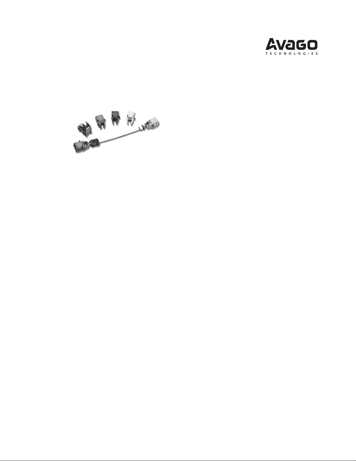
HFBR-0500Z Series
Versatile Link
The V ersa tile Fiber Optic Connection
Data Sheet
Description
The Versatile Link series is a
complete family of fiber optic link
components for applications
requiring a low cost solution. The
HFBR-0500Z series includes
transmitters, receivers, connectors and cable specified for easy
design. This series of components
is ideal for solving problems with
voltage isolation/insulation, EMI/
RFI immunity or data security.
The optical link design is simplified by the logic compatible
receivers and complete specifications for each component. The
key optical and electrical
parameters of links configured
with the HFBR-0500Z family are
fully guaranteed from 0° to 70°C.
A wide variety of package configurations and connectors provide
the designer with numerous
mechanical solutions to meet
application requirements. The
transmitter and receiver compo-
nents have been designed for use
in high volume/low cost assembly
processes such as auto insertion
and wave soldering.
Transmitters incorporate a 660
nm LED. Receivers include a
monolithic dc coupled, digital IC
receiver with open collector
Schottky output transistor. An
internal pullup resistor is available for use in the HFBR-25X1Z/
2Z/4Z receivers. A shield has been
integrated into the receiver IC to
provide additional, localized noise
immunity.
Internal optics have been optimized for use with 1 mm diameter
plastic optical fiber. Versatile Link
specifications incorporate all
connector interface losses.
Therefore, optical calculations for
common link applications are
simplified.
Features
• RoHS-compliant
• Low cost fiber optic components
• Enhanced digital links: dc-5 MBd
• Extended distance links up to
120 m at 40 kBd
• Low current link: 6 mA peak
supply current
• Horizontal and vertical mounting
• Interlocking feature
• High noise immunity
• Easy connectoring: simplex,
duplex, and latching connectors
• Flame retardant
• Transmitters incorporate a 660 nm
red LED for easy visibility
• Compatible with standard TTL
circuitry
Applications
• Reduction of lightning/voltage
transient susceptibility
• Motor controller triggering
• Data communications and local
area networks
• Electromagnetic Compatibility
(EMC) for regulated systems: FCC,
VDE, CSA, etc.
• Tempest-secure data processing
equipment
• Isolation in test and measurement
instruments
• Error free signalling for industrial
and manufacturing equipment
• Automotive communications and
control networks
• Noise immune communication in
audio and video equipment
Page 2
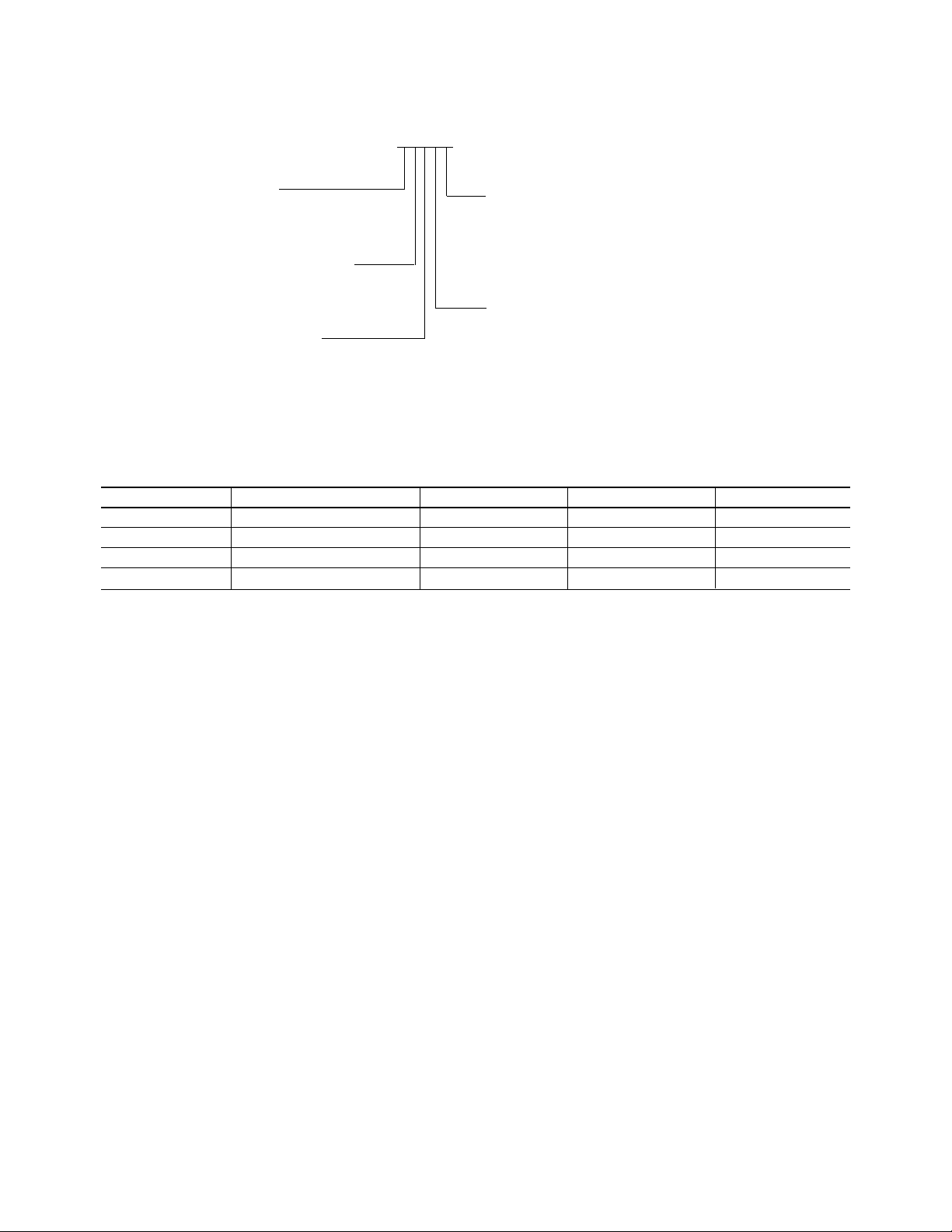
HFBR-0500Z Series Part Number Guide
HFBR X5XXZ
1 = Transmitter
2 = Receiver Z = RoHS-compliant
5 = 600 nm Transmitter and
Receiver Products 1 = 5 MBd High Performance Link
2 = 1 MBd High Performance Link
3 = 40 kBd Low Current/Extended Distance Link
2 = Horizontal Package 4 = 1 MBd Standard Link
3 = Vertical Package 6 = 155 MBd Receiver
7 = 155 MBd Transmitter
8 = 10 MBd High Performance Link
Link Selection Guide
(Links specified from 0 to 70°C, for plastic optical fiber unless specified.)
Signal Rate Distance (m) 25°C Distance (m) Transmitter Receiver
40 kBd 120 110 HFBR-1523Z HFBR-2523Z
1 MBd 20 10 HFBR-1524Z HFBR-2524Z
1 MBd 55 45 HFBR-1522Z HFBR-2522Z
5 Mbd 30 20 HFBR-1521Z HFBR-2521Z
Evaluation Kit
HFBR-0500Z 1 MBd Versatile Link:
This kit contains: HFBR-1524Z Tx, HFBR-2524Z Rx, polishing kit, 3 styles of plastic connectors, Bulkhead
feedthrough, 5 meters of 1 mm diameter plastic cable, lapping film and grit paper, and HFBR-0500Z data
sheet.
Application Literature
Application Note 1035 (Versatile Link)
Package and Handling Information
The compact Versatile Link package is made of a flame retardant
VALOX® UL 94 V-0 material
(UL file # E121562) and uses the
same pad layout as a standard,
eight pin dual-in-line package.
Vertical and horizontal mountable
parts are available. These low
profile Versatile Link packages
are stackable and are enclosed to
provide a dust resistant seal. Snap
action simplex, simplex latching,
duplex, and duplex latching
connectors are offered with
simplex or duplex cables.
Package Orientation
Performance and pinouts for the
vertical and horizontal packages
are identical. To provide additional attachment support for the
vertical Versatile Link housing,
the designer has the option of
using a self-tapping screw through
a printed circuit board into a
mounting hole at the bottom of
the package. For most
applications this is not necessary.
Package Housing Color
Versatile Link components and
simplex connectors are color
coded to eliminate confusion
VALOX® is a registered trademark of the General Electric Corporation.
2
Page 3
when making connections.
Receivers are blue and transmitters are gray, except for the
HFBR-15X3Z transmitter, which
is black.
Handling
Versatile Link components are
auto-insertable. When wave
soldering is performed with
Versatile Link components, the
optical port plug should be left in
to prevent contamination of the
port. Do not use reflow solder
processes (i.e., infrared reflow or
vapor-phase reflow).
Nonhalogenated water soluble
fluxes (i.e., 0% chloride), not rosin
based fluxes, are recommended
for use with Versatile Link
components.
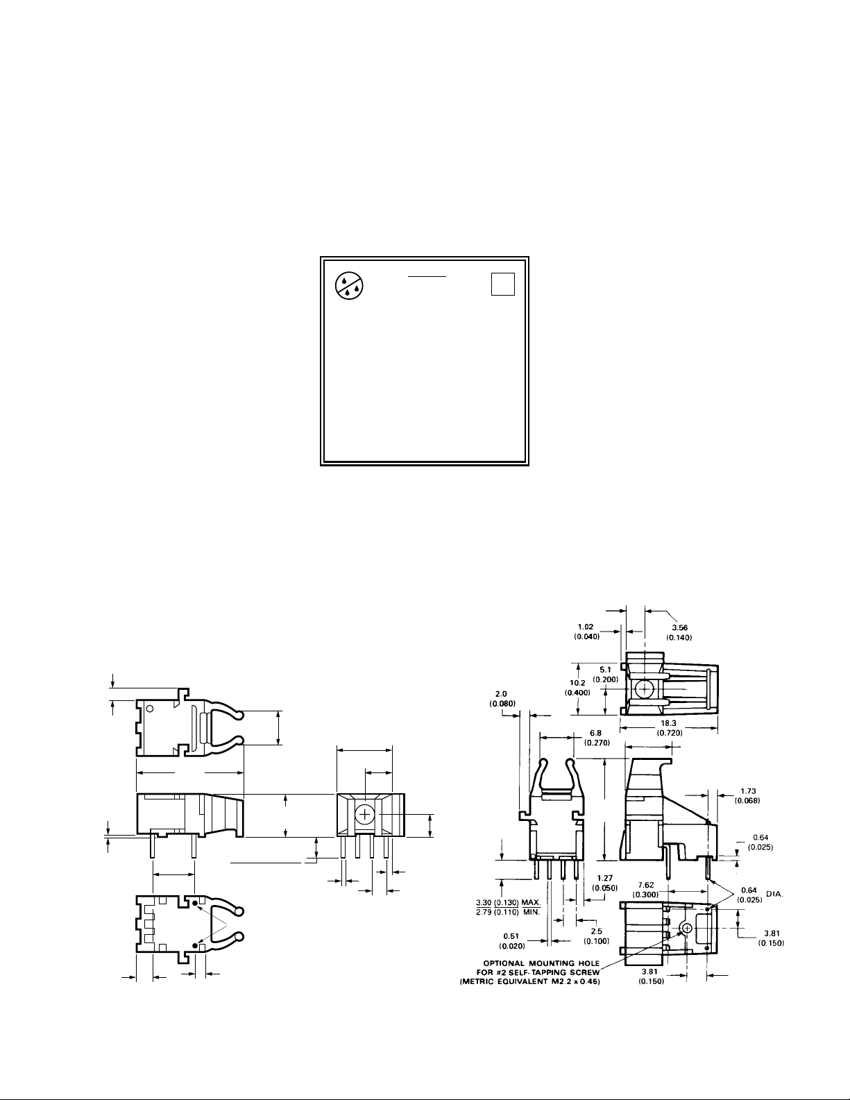
Versatile Link components are
moisture sensitive devices and are
shipped in a moisture sealed bag.
If the components are exposed to
air for an extended period of time,
they may require a baking step
before the soldering process.
Refer to the special labeling on
the shipping tube for details.
CAUTION
This bag contains
MOISTURE-SENSITIVE
DEVICES
1. Shelf life in sealed bag: 12 months at < 40°C and < 90% Relative
Humidity (RH).
2. After this bag is opened, devices that will be subjected to wave
soldering, or equivalent processing (solder temperature < 260°C for
10 sec) must be:
a) Mounted within 72 hours at factory conditions of ≤ 30°C/60% RH.
b) Stored at ≤ 20% RH.
3. Devices require baking, before mounting, if:
a) Desiccant changes to PINK.
b) If 2a or 2b are not met.
4. If baking is required, devices may be baked outside of tube for 20
hours at 75°C.
Bag Seal Date: ______________________________________________________
Note: LEVEL defined by EIA JEDEC Standard J-STD-020
(If blank, see barcode label)
Level
4
Recommended Chemicals for
Cleaning/Degreasing
Alcohols: methyl, isopropyl,
isobutyl. Aliphatics: hexane,
heptane. Other: soap solution,
naphtha.
Do not use partially halogenated
hydrocarbons such as 1,1.1
trichloroethane, ketones such as
MEK, acetone, chloroform, ethyl
acetate, methylene dichloride,
phenol, methylene chloride, or
N-methylpyrolldone. Also, Avago
does not recommend the use of
cleaners that use halogenated
hydrocarbons because of their
potential environmental harm.
Mechanical Dimensions
Horizontal Modules Vertical Modules
2.0
(0.080)
0.64
(0.025)
7.62
(0.300)
18.8
(0.740)
6.8
(0.270)
7.71
7.6
(0.305)
(0.30)
3.81 (0.150) MAX.
3.56 (0.140) MIN.
0.64 (0.025) DIA.
0.51
(0.020)
10.2
(0.400)
5.1
(0.200)
1.27
(0.050)
2.5
(0.100)
4.2
(0.165)
18.8
0.740
7.6
(0.30)
2.8
(0.109)
3
1.85
(0.073)
Page 4
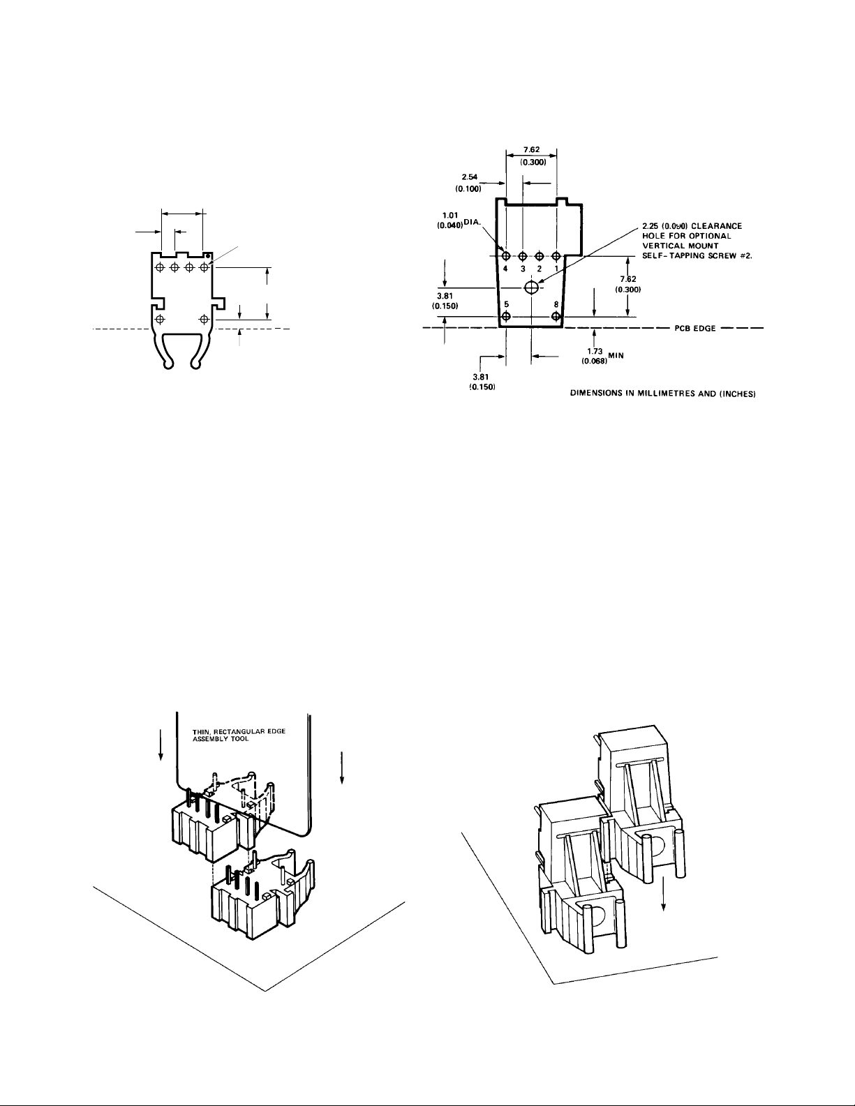
Versatile Link Printed Board Layout Dimensions
Horizontal Module Vertical Module
7.62
2.54
(0.100)
(0.300)
1.01 (0.040) DIA.
TOP VIEW
DIMENSIONS IN MILLIMETERS (INCHES).
4 13 2
5 6
1.85
(0.073)
7.62
(0.300)
MIN.
Interlocked (Stacked) Assemblies
(refer to Figure 1)
Horizontal packages may be
stacked by placing units with pins
facing upward. Initially engage
the interlocking mechanism by
sliding the L bracket body from
above into the L slot body of the
lower package. Use a straight
edge, such as a ruler, to bring all
PCB EDGE
stacked units into uniform
alignment. This technique
prevents potential harm that
could occur to fingers and hands
of assemblers from the package
pins. Stacked horizontal packages
can be disengaged if necessary.
Repeated stacking and unstacking
causes no damage to individual
units.
Stacking Horizontal Modules
Figure 1. Interlocked (stacked) horizontal or vertical packages.
4
Stacking Vertical Modules
Page 5
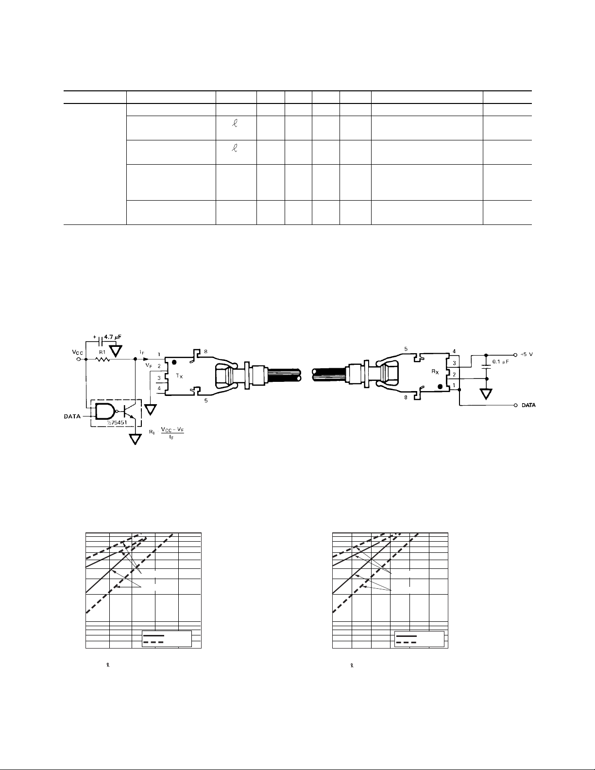
5 MBd Link (HFBR-15X1Z/25X1Z)
System Performance 0 to 70°C unless otherwise specified.
Parameter Symbol Min. Typ. Max. Units Conditions Ref.
High Data Rate dc 5 MBd BER ≤10-9, PRBS:27-1
Performance
5 MBd
Link Distance 19 m I
(Standard Cable) 27 48 m I
Link Distance 22 m I
(Improved Cable) 27 53 m I
Propagation t
Delay t
PLH
PHL
80 140 ns RL = 560 Ω, CL = 30 pF Fig. 5, 8
50 140 ns fiber length = 0.5 m Notes 1, 2
= 60 mA Fig. 3
Fdc
= 60 mA, 25°C Note 3
Fdc
= 60 mA Fig. 4
Fdc
= 60 mA, 25°C Note 3
Fdc
-21.6 ≤PR ≤-9.5 dBm
Pulse Width t
Distortion t
PLH-tPHL
D
Notes:
1. The propagation delay for one metre of cable is typically 5 ns.
2. Typical propagation delay is measured at P
= -15 dBm.
R
3. Estimated typical link life expectancy at 40°C exceeds 10 years at 60 mA.
30 ns PR = -15 dBm Fig. 5, 7
RL = 560 Ω, CL = 30 pF
Figure 2. Typical 5 MBd interface circuit.
100
50
40
30
20
10
F
I – FORWARD CURRENT (mA)
5
01020304050
– CABLE LENGTH – METRES
OVERDRIVE
UNDERDRIVE
0°C–70°C
25°C
Figure 3. Guaranteed system performance with standard cable
(HFBR-15X1Z/25X1Z).
5
100
50
40
30
20
10
F
I – FORWARD CURRENT (mA)
5
01020304050
– CABLE LENGTH – METRES
OVERDRIVE
UNDERDRIVE
0°C–70°C
25°C
60
Figure 4. Guaranteed system performance with improved cable
(HFBR-15X1Z/25X1Z).
Page 6
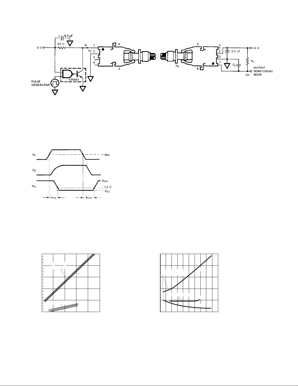
Figure 5. 5 MBd propagation delay test circuit.
Figure 6. Propagation delay test waveforms.
500
HFBR-15X2Z/25X2Z
400
HFBR-15X4Z/25X4Z
300
200
100
– PULSE WIDTH DISTORTION – ns
D
t
HFBR-15X1Z/25X1Z
0
-25
-20 -15 -5
PR – INPUT OPTICAL POWER – dBm
6
70°C
25°C
0°C
70°C
25°C
0°C
-10 0
500
400
HFBR-15X2Z/25X2Z
HFBR-15X4Z/25X4Z
300
200
HFBR-15X1Z/25X1Z
100
– PROPAGATION DELAY – ns
p
t
0
-25
-20 -15 -5
PR – INPUT OPTICAL POWER – dBm
Figure 8. Typical link propagation delay vs. optical power.Figure 7. Typical link pulse width distortion vs. optical power.
t
pLH
t
pLH
t
pHL
-10 0
Page 7
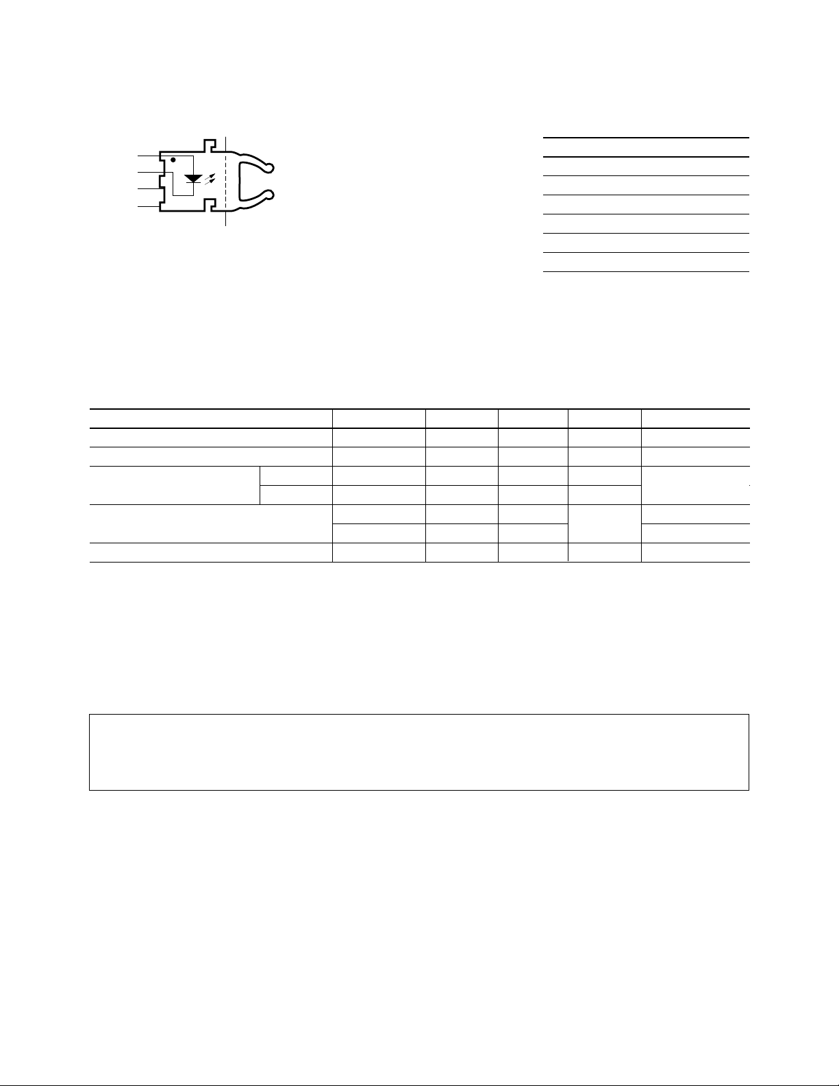
HFBR-15X1Z Transmitter
ANODE
CATHODE
N.C.
N.C.
1
8 DO NOT CONNECT
2
3
4
5 DO NOT CONNECT
Pin # Function
1 Anode
2 Cathode
3 Open
4 Open
5 Do not connect
8 Do not connect
Note: Pins 5 and 8 are for mounting and
retaining purposes only. Do not electrically
connect these pins.
Absolute Maximum Ratings
Parameter Symbol Min. Max. Units Reference
Storage Temperature T
Operating Temperature T
S
A
–40 +85 °C
–40 +85 °C
Lead Soldering Cycle Temp. 260 °C Note 1
Time 10 sec
Forward Input Current I
Reverse Input Voltage V
FPK
I
Fdc
BR
1000 mA Note 2, 3
80
5V
Notes:
1. 1.6 mm below seating plane.
2. Recommended operating range between 10 and 750 mA.
3. 1 µs pulse, 20 µs period.
All HFBR-15XXZ LED transmitters are classified as IEC 825-1 Accessible Emission Limit (AEL) Class 1
based upon the current proposed draft scheduled to go into effect on January 1, 1997. AEL Class 1 LED
devices are considered eye safe. Contact your local Avago sales representative for more information.
7
Page 8
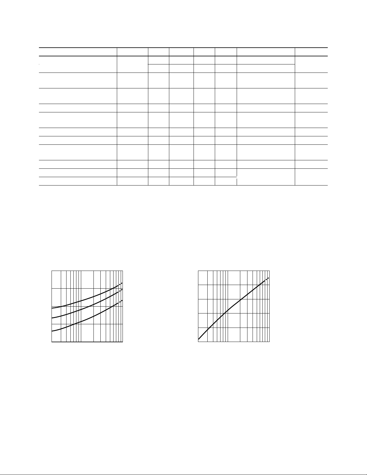
Transmitter Electrical/Optical Characteristics 0°C to 70°C unless otherwise specified.
Parameter Symbol Min. Typ.
Transmitter Output P
Optical Power
T
-16.5 -7.6 dBm I
-14.3 -8.0 dBm I
[5]
Max. Units Conditions Ref.
= 60 mA Notes 1, 2
Fdc
= 60 mA, 25°C
Fdc
Output Optical Power ∆PT/∆T-0.85 %/°C
Temperature Coefficient
Peak Emission λ
PK
660 nm
Wavelength
Forward Voltage V
F
1.45 1.67 2.02 V I
= 60 mA
Fdc
Forward Voltage ∆VF/∆T -1.37 mV/°C Fig. 9
Temperature Coefficient
Effective Diameter D 1 mm
Numerical Aperture NA 0.5
Reverse Input Breakdown V
BR
5.0 11.0 V I
= 10 µA,
Fdc
Voltage TA = 25°C
Diode Capacitance C
Rise Time t
Fall Time t
O
r
f
Notes:
1. Measured at the end of 0.5 m standard fiber optic cable with large area detector.
2. Optical power, P (dBm) = 10 Log [P(µW)/1000 µW].
3. Rise and fall times are measured with a voltage pulse driving the transmitter and a series connected 50 Ω load. A wide bandwidth optical to
electrical waveform analyzer, terminated to a 50 Ω input of a wide bandwidth oscilloscope, is used for this response time measurement.
86 pF VF = 0, f = MHz
80 ns 10% to 90%, Note 3
40 ns
IF = 60 mA
1.8
1.7
1.6
1.5
– FORWARD VOLTAGE – V
F
V
1.4
2
I
– TRANSMITTER DRIVE CURRENT (mA)
Fdc
10
0°C
25°C
70°C
100
5
0
-5
-10
-15
– NORMALIZED OUTPUT POWER – dB
T
P
-20
2
I
– TRANSMITTER DRIVE CURRENT (mA)
Fdc
10
100
Figure 9. Typical forward voltage vs. drive current. Figure 10. Normalized typical output power vs. drive current.
8
Page 9
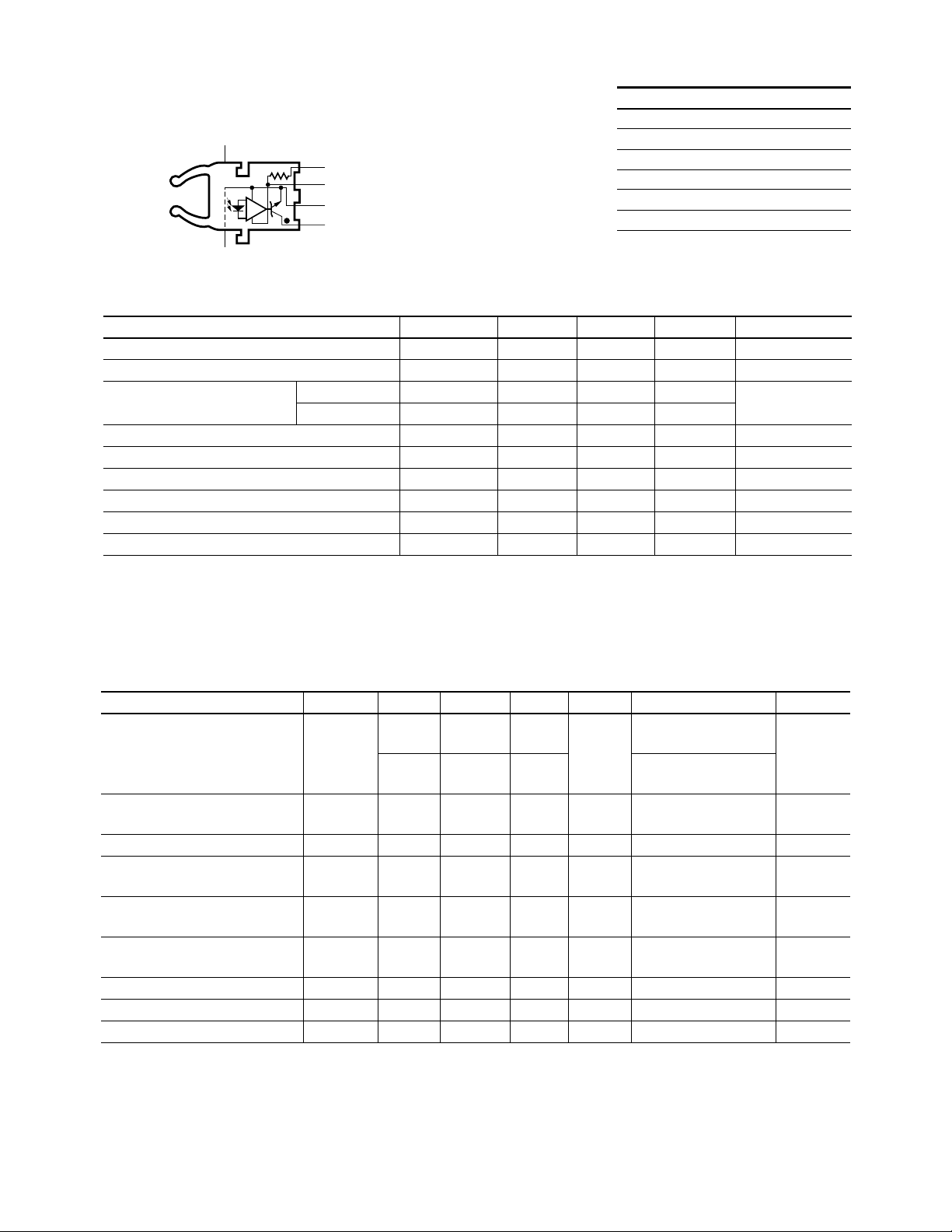
HFBR-25X1Z Receiver
DO NOT CONNECT 5
DO NOT CONNECT 8
1000 Ω
4
3
2
1
R
L
V
CC
GROUND
V
O
Pin # Function
1V
O
2 Ground
3V
4R
CC
L
5 Do not connect
8 Do not connect
Note: Pins 5 and 8 are for mounting and
retaining purposes only. Do not electrically
connect these pins.
Absolute Maximum Ratings
Parameter Symbol Min. Max. Units Reference
Storage Temperature T
Operating Temperature T
S
A
–40 +85 °C
–40 +85 °C
Lead Soldering Cycle Temp. 260 °C Note 1
Time 10 sec
Supply Voltage V
Output Collector Current I
Output Collector Power Dissipation P
Output Voltage V
Pull-up Voltage V
CC
OAV
OD
O
P
–0.5 7 V Note 2
25 mA
40 mW
–0.5 18 V
–5 V
CC
V
Fan Out (TTL) N 5
Notes:
1. 1.6 mm below seating plane.
2. It is essential that a bypass capacitor 0.01 µF be connected from pin 2 to pin 3 of the receiver. Total lead length between both ends of the capacitor
and the pins should not exceed 20 mm.
Receiver Electrical/Optical Characteristics
0°C to 70°C, 4.75 V ≤VCC ≤5.25 V unless otherwise specified
Parameter Symbol Min. Typ. Max. Units Conditions Ref.
Input Optical Power P
R(L)
–21.6 –9.5 dBm VOL = 0.5 V Notes 1,
Level for Logic “0” IOL = 8 mA 2, 4
–21.6 –8.7 VOL = 0.5 V
IOL = 8 mA, 25°C
Input Optical Power P
R(H)
–43 dBm VOL = 5.25 V Note 1
Level for Logic “1” IOH ≤250 µA
High Level Output Current I
Low Level Output Current V
High Level Supply I
OH
OL
CCH
5 250 µAVO = 18 V, PR = 0 Note 3
0.4 0.5 V IOL = 8 mA, Note 3
PR = P
R(L)MIN
3.5 6.3 mA VCC = 5.25 V, Note 3
Current PR = 0
Low Level Supply Current I
CCL
6.2 10 mA VCC = 5.25 V Note 3
PR = -12.5 dBm
Effective Diameter D 1 mm
Numerical Aperture NA 0.5
Internal Pull-up Resistor R
Notes:
1. Optical flux, P (dBm) = 10 Log [P (µW)/1000 µW].
2. Measured at the end of the fiber optic cable with large area detector.
3. RL is open.
4. Pulsed LED operation at IF > 80 mA will cause increased link t
width distortion of the receiver output signal.
L
680 1000 1700 Ω
propagation delay time. This extended t
PLH
time contributes to increased pulse
PLH
9
Page 10
1 MBd Link
(High Performance HFBR-15X2Z/25X2Z, Standard HFBR-15X4Z/25X4Z)
System Performance Under recommended operating conditions unless otherwise specified.
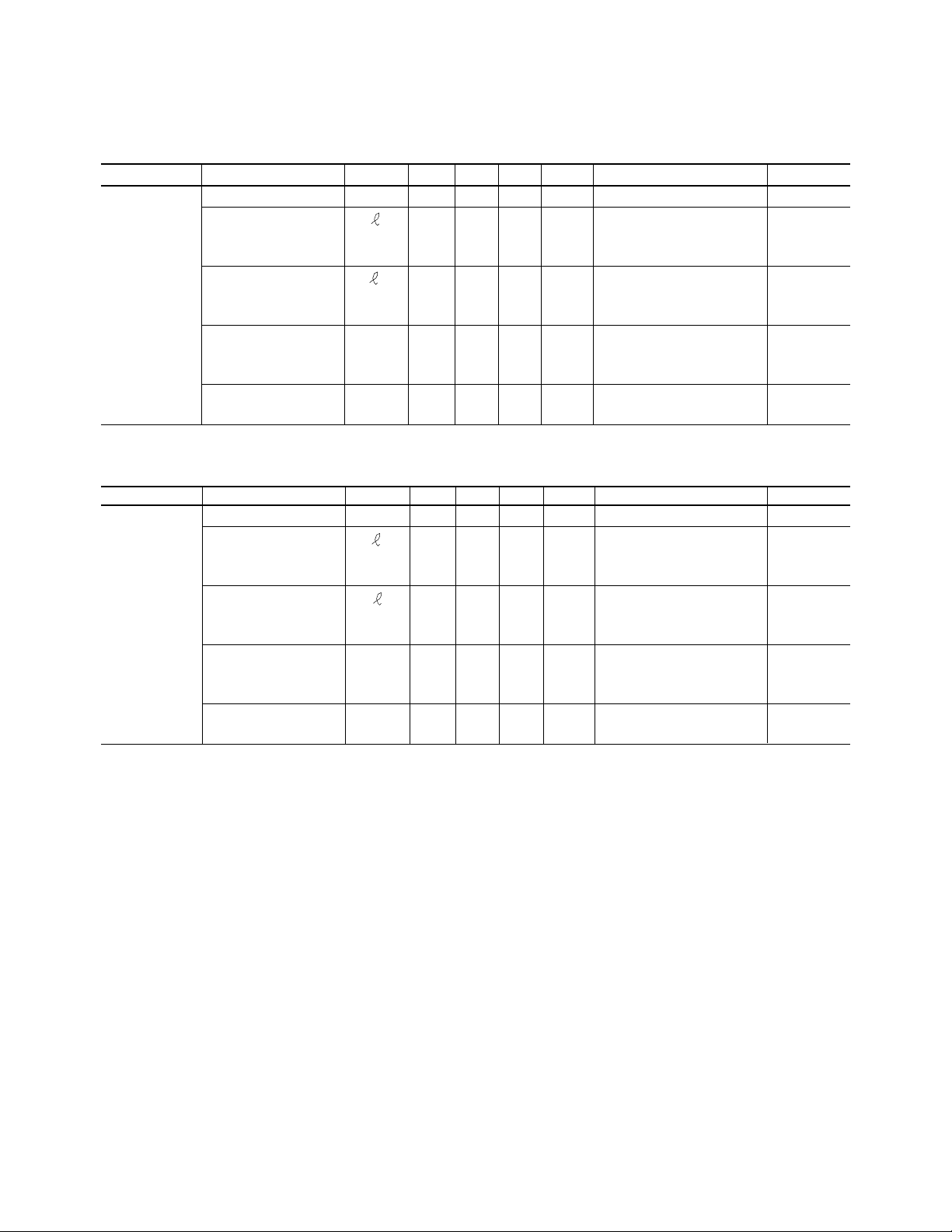
Parameter Symbol Min. Typ. Max. Units Conditions Ref.
High Data Rate dc 1 MBd BER ≤10-9, PRBS:27-1
Performance
1 MBd
Link Distance 39 m I
(Standard Cable) 47 70 m I
Link Distance 45 m I
(Improved Cable) 56 78 m I
Propagation t
Delay t
PLH
PHL
180 250 ns RL = 560 Ω, CL = 30 pF Fig. 16, 18
100 140 ns I = 0.5 metre Notes 2, 4
= 60 mA Fig. 14
Fdc
= 60 mA, 25°C Notes 1,
Fdc
= 60 mA Fig. 15
Fdc
= 60 mA, 25°C Notes 1,
Fdc
PR = -24 dBm
Pulse Width t
Distortion t
PLH-tPHL
D
80 ns PR = -24 dBm Fig. 16, 17
RL = 560 Ω, CL = 30 pF Note 4
Parameter Symbol Min. Typ. Max. Units Conditions Ref.
Standard Data Rate dc 1 MBd BER ≤10-9, PRBS:27-1
1 MBd
Link Distance 8 m I
(Standard Cable) 17 43 m I
Link Distance 10 m I
(Improved Cable) 19 48 m I
Propagation t
Delay t
PLH
PHL
180 250 ns RL = 560 Ω, CL = 30 pF Fig. 16, 18
100 140 ns I = 0.5 metre Notes 2, 4
= 60 mA Fig. 12
Fdc
= 60 mA, 25°C Notes 1,
Fdc
= 60 mA Fig. 13
Fdc
= 60 mA, 25°C Notes 1,
Fdc
PR = -20 dBm
Pulse Width t
Distortion t
Notes:
1. For I
2. The propagation delay for one meter of cable is typically 5 ns.
3. Estimated typical link life expectancy at 40°C exceeds 10 years at 60 mA.
4. Pulsed LED operation at I
> 80 mA, the duty factor must be such as to keep I
FPK
I
≤160 mA: Pulse width ≤1 ms
FPK
I
> 160 mA: Pulse width ≤1 µS, period ≥20 µS.
FPK
width distortion of the receiver output signal.
PLH-tPHL
> 80 mA will cause increased link t
FPK
D
≤80 mA. In addition, for I
Fdc
80 ns PR = -20 dBm Fig. 16, 17
RL = 560 Ω, CL = 30 pF Note 4
> 80 mA, the following rules for pulse width apply:
FPK
propagation delay time. This extended t
PLH
time contributes to increased pulse
PLH
3, 4
3, 4
3, 4
3, 4
10
Page 11
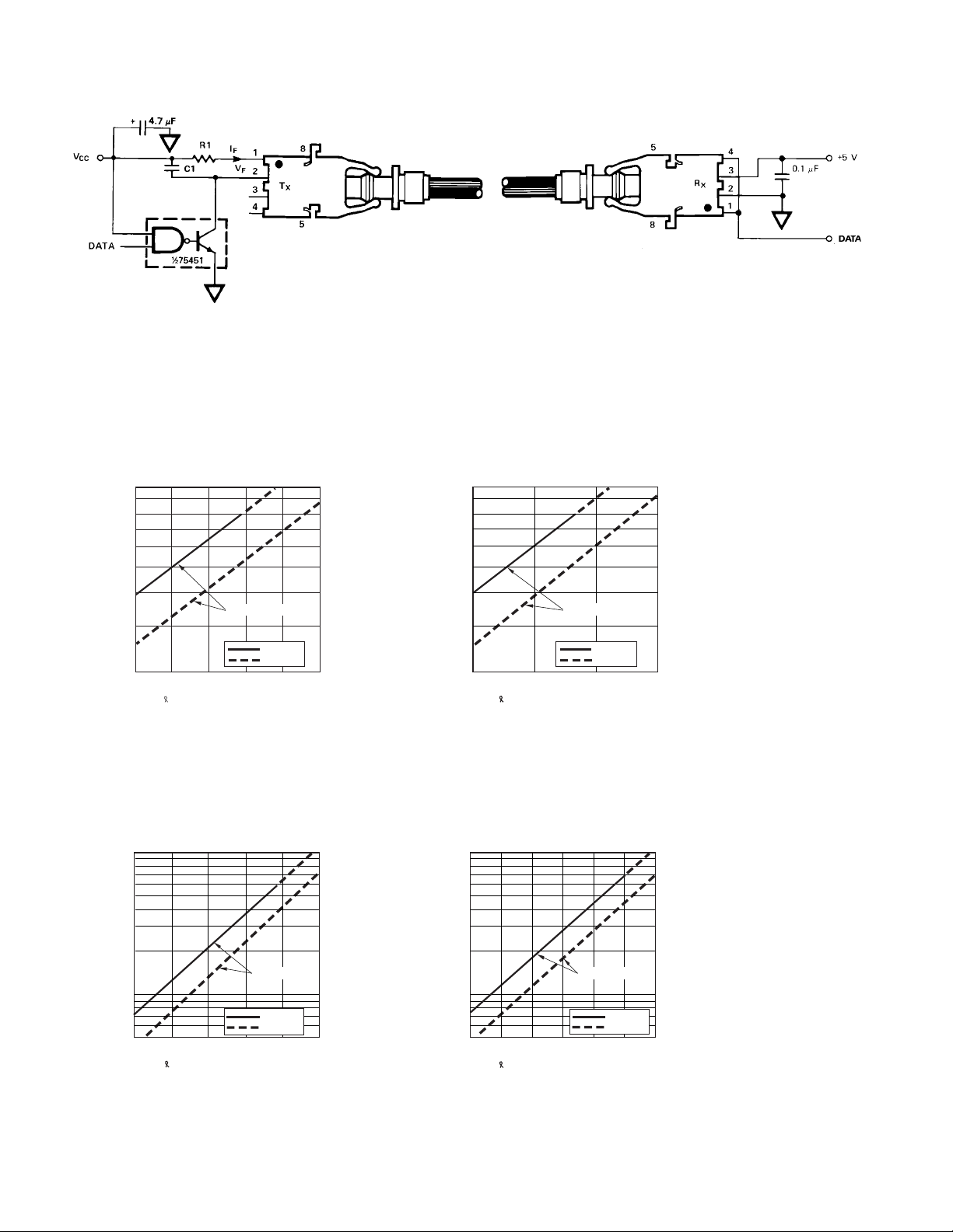
Figure 11. Required 1 MBd interface circuit.
The HFBR-25X2Z receiver can not be overdriven when using the required
interface circuit shown in Figure 11.
100
90
80
70
60
50
40
HFBR-15X4Z/25X4Z
30
F
I – FORWARD CURRENT (mA)
20
05 2010 2515
– CABLE LENGTH – METRES
0°C–70°C
25°C
Figure 12. Guaranteed system performance for the
HFBR-15X4Z/25X4Z link with standard cable.
100
50
40
30
20
UNDERDRIVE
10
F
I – FORWARD CURRENT (mA)
5
01020304050
– CABLE LENGTH – METRES
0°C–70°C
25°C
100
90
80
70
60
50
40
HFBR-15X4Z/25X4Z
30
F
I – FORWARD CURRENT (mA)
20
02010 30
– CABLE LENGTH – METRES
0°C–70°C
25°C
Figure 13. Guaranteed system performance for the
HFBR-15X4Z/25X4Z link with improved cable.
100
50
40
30
20
UNDERDRIVE
10
F
I – FORWARD CURRENT (mA)
5
01020304050
– CABLE LENGTH – METRES
0°C–70°C
25°C
60
Figure 14. Guaranteed system performance for the
HFBR-15X2Z/25X2Z link with standard cable.
11
Figure 15. Guaranteed system performance for the
HFBR-15X2Z/25X2Z link with improved cable.
Page 12
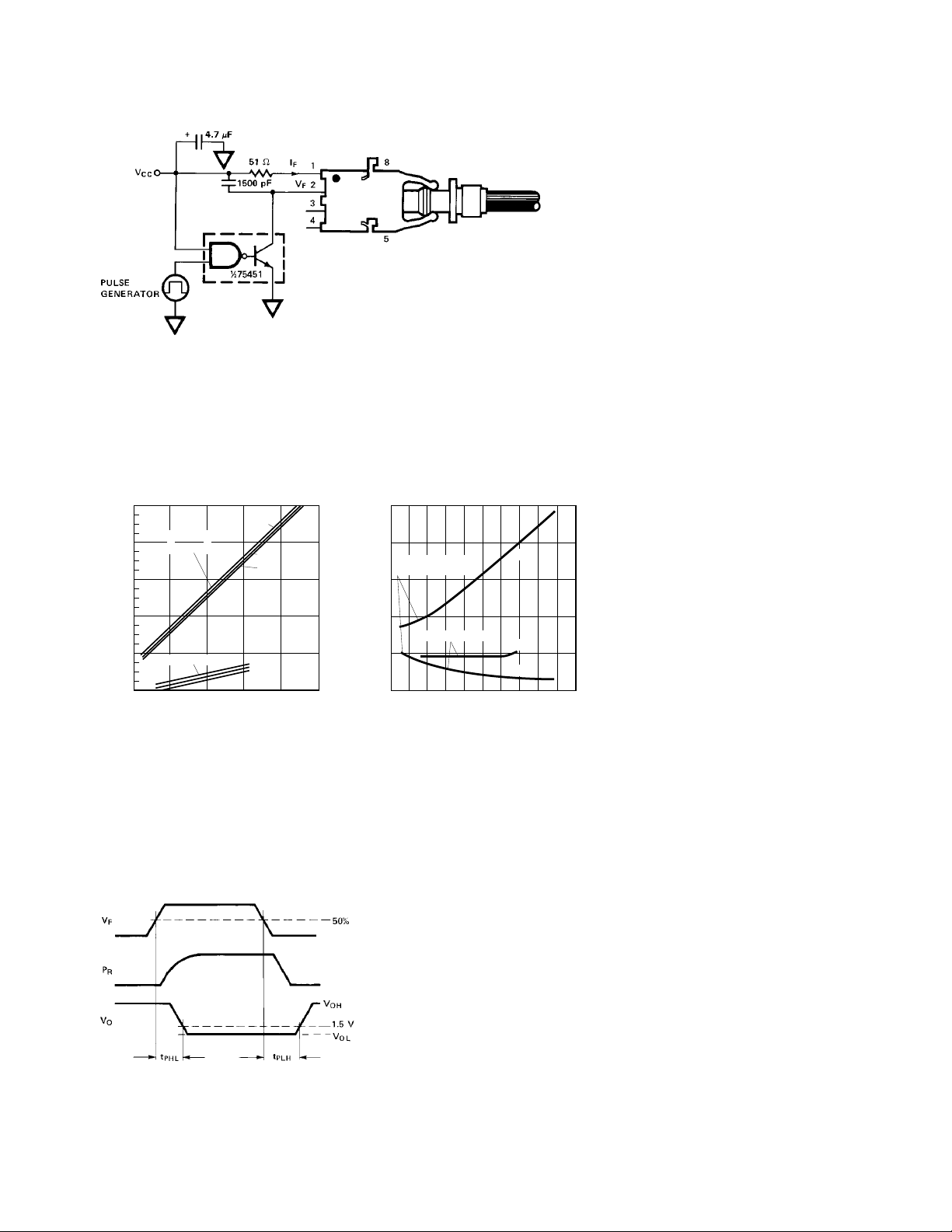
Figure 16. 1 MBd propagation delay test circuit.
500
HFBR-15X2Z/25X2Z
400
HFBR-15X4Z/25X4Z
300
200
100
– PULSE WIDTH DISTORTION – ns
D
t
HFBR-15X1Z/25X1Z
0
-20 -15 -5
-25
PR – INPUT OPTICAL POWER – dBm
70°C
25°C
0°C
70°C
25°C
0°C
-10 0
Figure 17. Pulse width distortion vs. optical
power.
500
400
HFBR-15X2Z/25X2Z
HFBR-15X4Z/25X4Z
300
200
HFBR-15X1Z/25X1Z
100
– PROPAGATION DELAY – ns
p
t
0
-20 -15 -5
-25
PR – INPUT OPTICAL POWER – dBm
t
pLH
t
pLH
t
pHL
-10 0
Figure 18. Typical link propagation delay vs.
optical power.
Figure 19. Propagation delay test waveforms.
12
Page 13
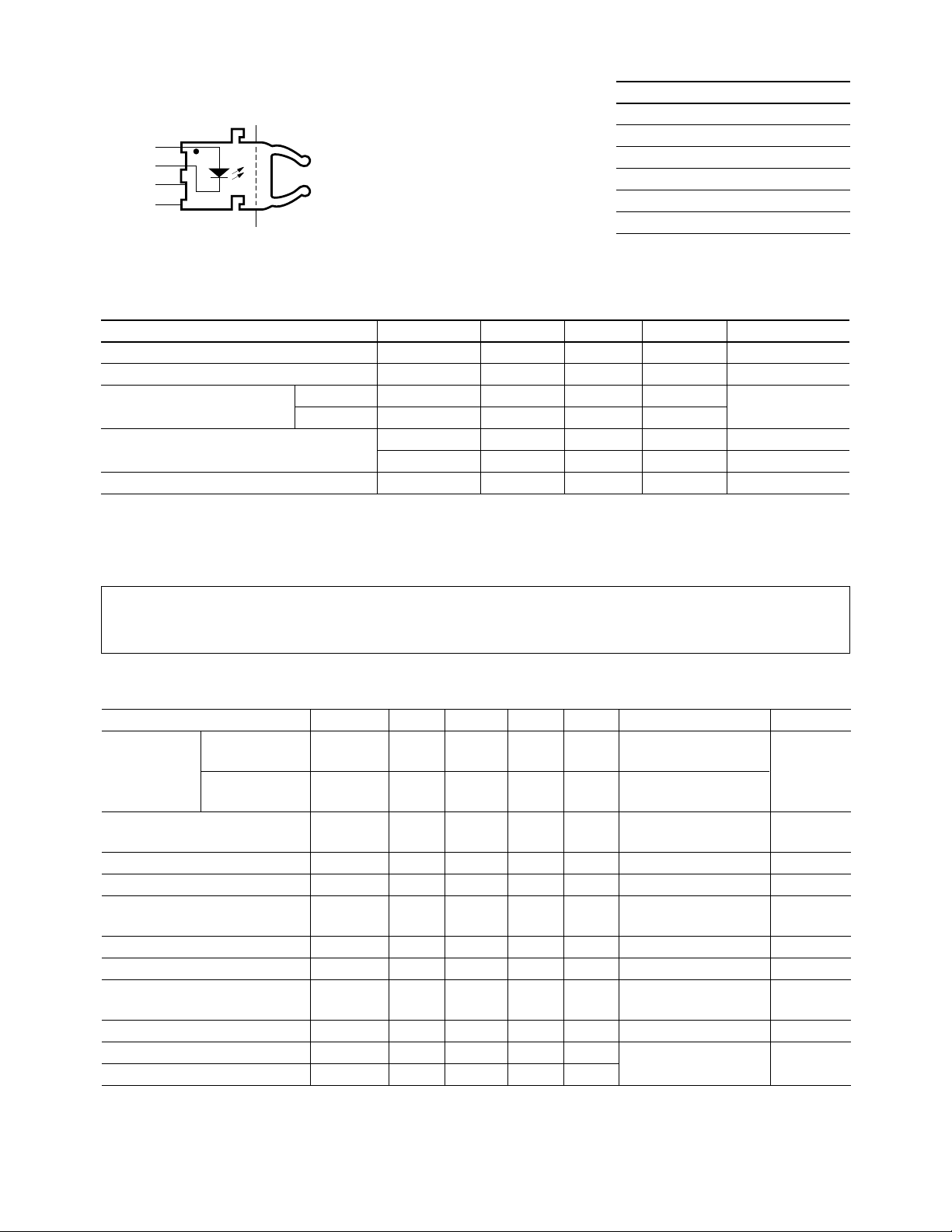
HFBR-15X2Z/15X4Z Transmitters
8 DO NOT CONNECT
5 DO NOT CONNECT
ANODE
CATHODE
N.C.
N.C.
1
2
3
4
Pin # Function
1 Anode
2 Cathode
3 Open
4 Open
5 Do not connect
8 Do not connect
Note: Pins 5 and 8 are for mounting and
retaining purposes only. Do not electrically
connect these pins.
Absolute Maximum Ratings
Parameter Symbol Min. Max. Units Reference
Storage Temperature T
Operating Temperature T
S
A
–40 +85 °C
–40 +85 °C
Lead Soldering Cycle Temp. 260 °C Note 1
Time 10 sec
Forward Input Current I
Reverse Input Voltage V
Notes:
1. 1.6 mm below seating plane.
2. Recommended operating range between 10 and 750 mA.
3. 1 µs pulse, 20 µs period.
I
FPK
Fdc
BR
1000 mA Note 2, 3
80
5V
All HFBR-15XXZ LED transmitters are classified as IEC 825-1 Accessible Emission Limit (AEL) Class 1 based upon
the current proposed draft scheduled to go into effect on January 1, 1997. AEL Class 1 LED devices are considered
eye safe. Contact your Avago sales representative for more information.
Transmitter Electrical/Optical Characteristics 0°C to 70°C unless otherwise specified.
For forward voltage and output power vs. drive current graphs.
Parameter Symbol Min. Typ. Max. Units Conditions Ref.
Transmitter HFBR-15X2Z P
T
Output –11.2 –5.1 I
Optical HFBR-15X4Z P
T
Power –15.5 –5.1 I
–13.6 –4.5 dBm I
–17.8 –4.5 dBm I
= 60 mA
Fdc
= 60 mA, 25°C
Fdc
= 60 mA
Fdc
= 60 mA, 25°C
Fdc
Output Optical Power ∆PT/∆T–0.85 %/°C
Temperature Coefficient
Peak Emission Wavelength λ
Forward Voltage V
PK
F
1.45 1.67 2.02 V I
660 nm
= 60 mA
Fdc
Forward Voltage ∆VF/∆T–1.37 mV/°C Fig. 11
Temperature Coefficient
Effective Diameter D
T
1mm
Numerical Aperture NA 0.5
Reverse Input Breakdown V
BR
5.0 11.0 V I
= 10 µA,
Fdc
Voltage TA = 25°C
Diode Capacitance C
Rise Time t
Fall Time t
Note:
1. Rise and fall times are measured with a voltage pulse driving the transmitter and a series connected 50 Ω load. A wide bandwidth optical to
electrical waveform analyzer, terminated to a 50 Ω input of a wide bandwidth oscilloscope, is used for this response time measurement.
O
r
f
86 pF VF = 0, f = 1 MHz
80 ns 10% to 90%, Note 1
40 ns IF = 60 mA
13
Page 14
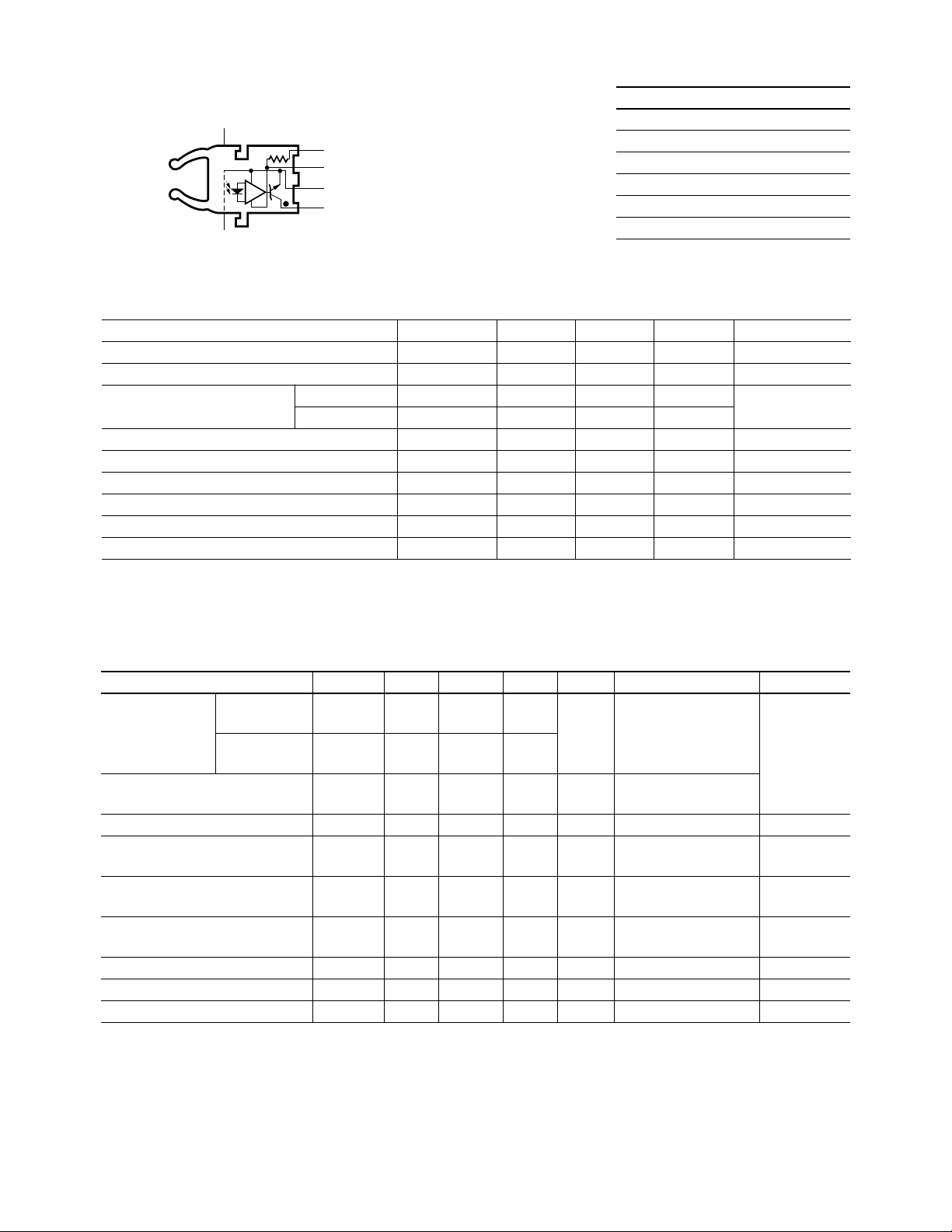
HFBR-25X2Z/25X4Z Receivers
DO NOT CONNECT 5
1000 Ω
DO NOT CONNECT 8
4
3
2
1
R
L
V
CC
GROUND
V
O
Pin # Function
1V
O
2 Ground
3V
4R
CC
L
5 Do not connect
8 Do not connect
Note: Pins 5 and 8 are for mounting and
retaining purposes only. Do not electrically
connect these pins.
Absolute Maximum Ratings
Parameter Symbol Min. Max. Units Reference
Storage Temperature T
Operating Temperature T
S
A
–40 +85 °C
–40 +85 °C
Lead Soldering Cycle Temp. 260 °C Note 1
Time 10 sec
Supply Voltage V
Output Collector Current I
Output Collector Power Dissipation P
Output Voltage V
Pull-up Voltage V
CC
OAV
OD
O
P
–0.5 7 V Note 2
25 mA
40 mW
–0.5 18 V
–5 V
CC
V
Fan Out (TTL) N 5
Notes:
1. 1.6 mm below seating plane.
2. It is essential that a bypass capacitor 0.01 µF be connected from pin 2 to pin 3 of the receiver. Total lead length between both ends of the capacitor
and the pins should not exceed 20 mm.
Receiver Electrical/Optical Characteristics 0°C to 70°C, 4.75 V ≤VCC ≤5.25 V unless otherwise specified.
Parameter Symbol Min. Typ. Max. Units Conditions Ref.
Receiver HFBR-2522Z P
R(L)
–24 dBm VOL = 0 V Notes 1, 2, 3
Optical Input IOL = 8 mA
Power Level HFBR-2524Z –20 Note 4
Logic 0
Optical Input Power P
R(H)
-43 dBm VOH = 5.25 V
Level Logic 1 IOH = ≤250 µA
High Level Output Current I
Low Level Output Voltage V
High Level Supply Current I
OH
OL
CCH
5 250 µAVO = 18 V, PR = 0 Note 5
0.4 0.5 V IOL = 8 mA Note 5
PR = P
R(L)MIN
3.5 6.3 mA VCC = 5.25 V, Note 5
PR = 0
Low Level Supply Current I
CCL
6.2 10 mA VCC = 5.25 V, Note 5
PR = -12.5 dBm
Effective Diameter D 1 mm
Numerical Aperture NA 0.5
Internal Pull-up Resistor R
Notes:
1. Measured at the end of the fiber optic cable with large area detector.
2. Pulsed LED operation at IF > 80 mA will cause increased link t
width distortion of the receiver output signal.
3. The LED drive circuit of Figure 11 is required for 1 MBd operation of the HFBR-25X2Z/25X4Z.
4. Optical flux, P (dBm) = 10 Log [P(µW)/1000 µW].
5. RL is open.
L
680 1000 1700 Ω
propagation delay time. This extended t
PLH
time contributes to increased pulse
PLH
14
Page 15
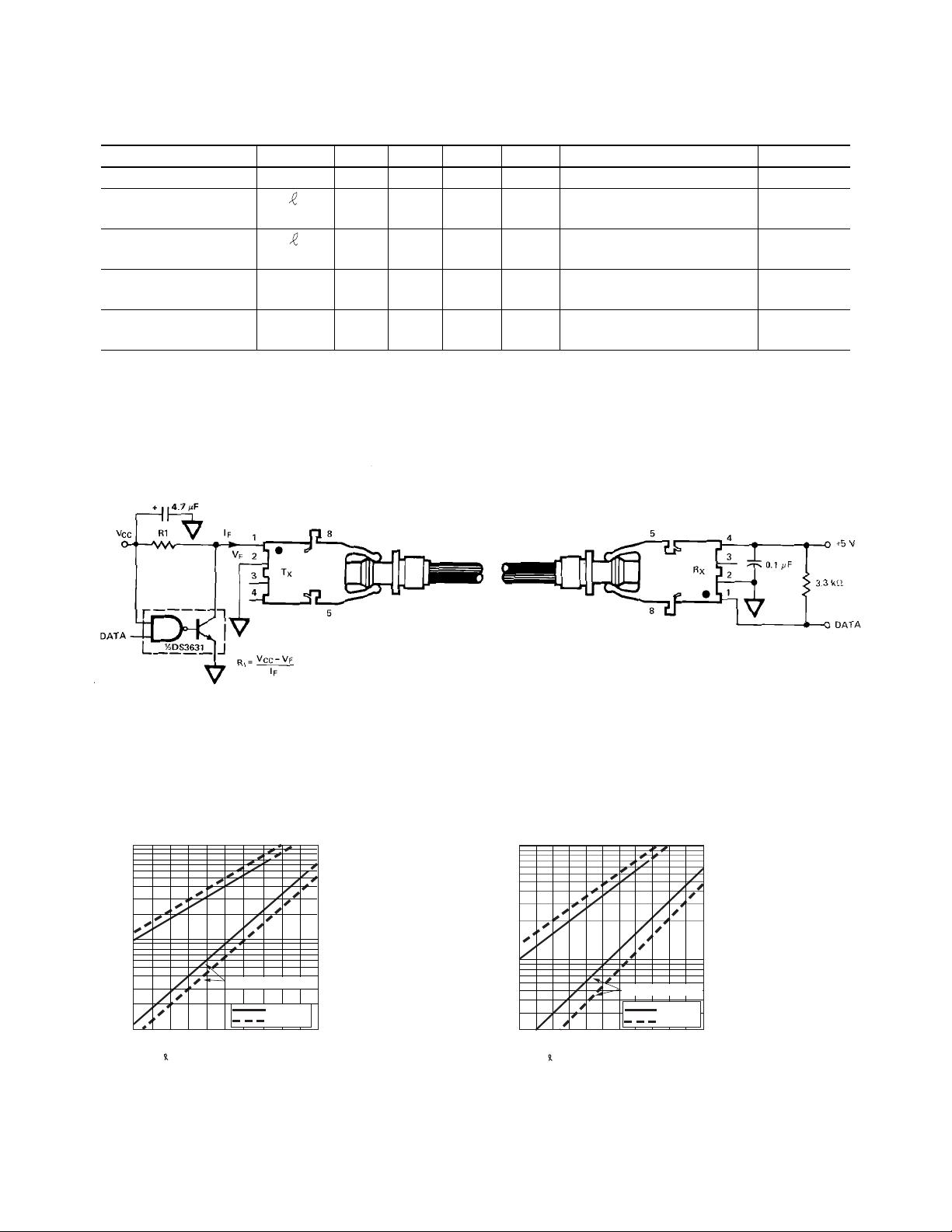
40 kBd Link
System Performance Under recommended operating conditions unless otherwise specified.
Parameter Symbol Min. Typ. Max. Units Conditions Ref.
Data Rate dc 40 kBd BER ≤10-9, PRBS: 27 - 1
Link Distance 13 41 m I
(Standard Cable) 94 138 m I
Link Distance 15 45 m I
(Improved Cable) 111 154 m I
Propagation t
Delay t
Pulse Width t
Distortion t
PLH-tPHL
PLH
PHL
D
Notes:
1. Estimated typical link life expectancy at 40°C exceeds 10 years at 60 mA.
2. The propagation delay for one metre of cable is typically 5 ns.
4 µsRL = 3.3 kΩ, CL = 30 pF Fig. 22, 25
2.5 µsPR = -25 dBm, 1 m fiber Note 2
7 µs -39 ≤PR≤- 14 dBm Fig. 23, 24
= 2 mA Fig. 21
Fdc
= 60 mA Note 1
Fdc
= 2 mA Fig. 22
Fdc
= 60 mA Note 1
Fdc
RL = 3.3 kΩ, CL = 30 pF
Figure 20. Typical 40 kBd interface circuit.
120
100
80
60
40
20
10
6
4
F
I – FORWARD CURRENT (mA)
2
1
01020304050
– CABLE LENGTH – METRES
HFBR-15X3Z/25X3Z
0°C–70°C
25°C
70 80 90 100
60
Figure 21. Guaranteed system performance with
standard cable.
15
120
100
80
60
40
20
10
6
4
F
I – FORWARD CURRENT (mA)
2
01020304050
– CABLE LENGTH – METRES
HFBR-15X3Z/25X3Z
0°C–70°C
25°C
60 70 80 90 100
110
Figure 22. Guaranteed system performance with
improved cable.
Page 16
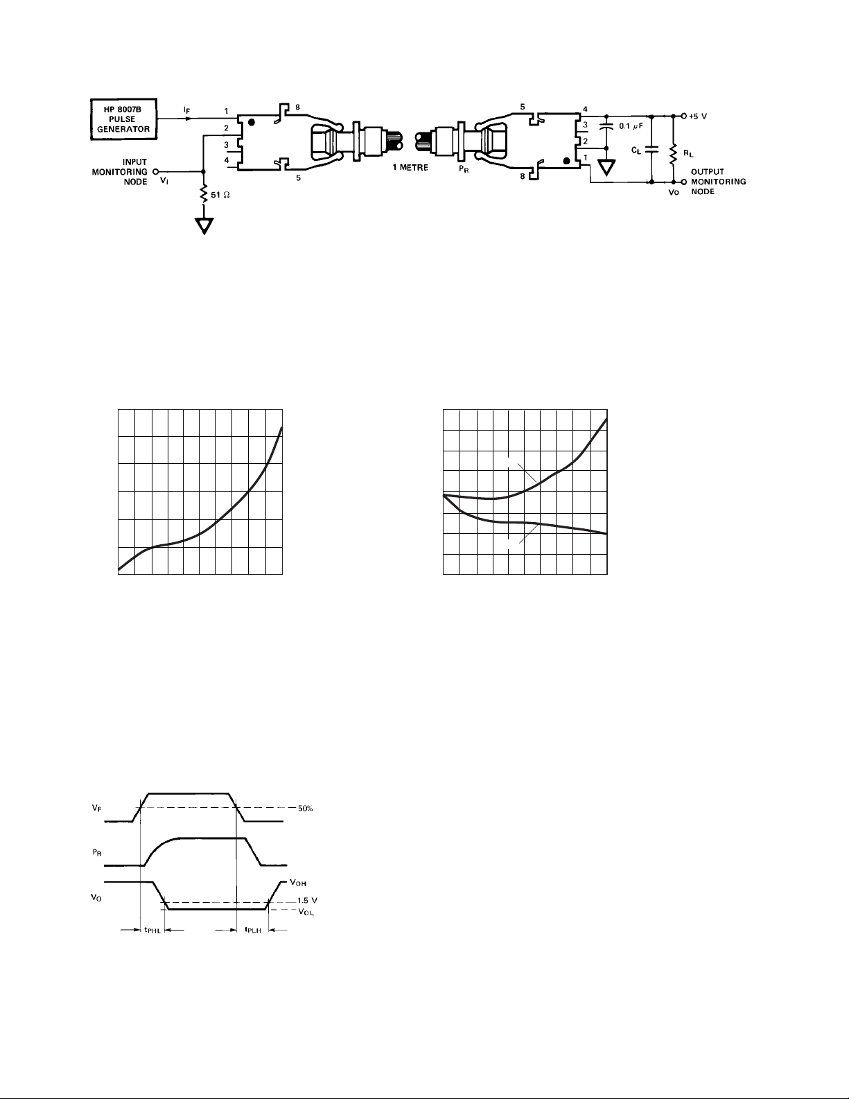
Figure 23. 40 kBd propagation delay test circuit.
6
5
4
3
2
1
D
t – PULSE WIDTH DISTORTION – µs
0
-40 -28-34 -10
P – INPUT OPTICAL POWER, dBm
R
-22 -16
8
7
6
5
4
3
2
P
t – PROPAGATION DELAY – µs
1
0
-40 -28-34 -10
t
PLH
t
PHL
-22 -16
P – INPUT OPTICAL POWER, dBm
R
Figure 25. Typical link propagation delay vs. optical power.Figure 24. Typical link pulse width distortion vs. optical power.
Figure 26. Propagation delay test waveforms.
16
Page 17
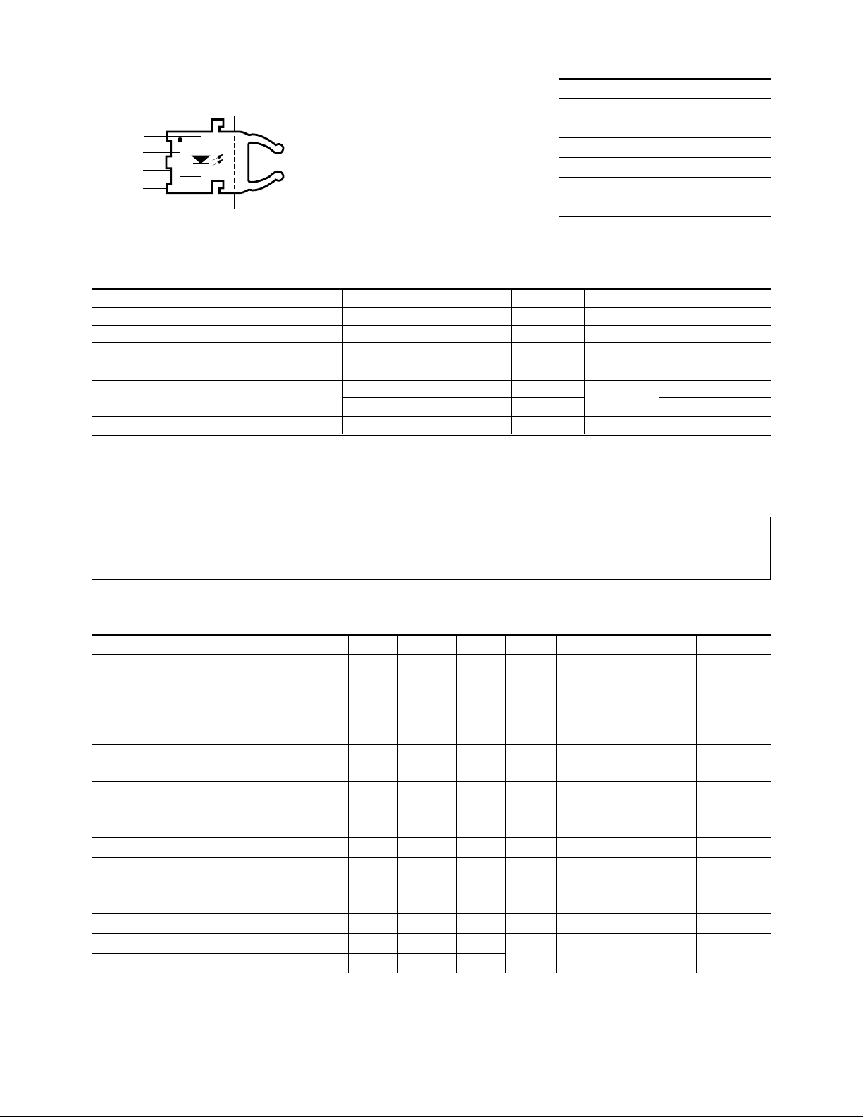
HFBR-15X3Z Transmitter
N.C.
N.C.
1
2
3
4
ANODE
CATHODE
8 DO NOT CONNECT
5 DO NOT CONNECT
Pin # Function
1 Anode
2 Cathode
3 Open
4 Open
5 Do not connect
8 Do not connect
Note: Pins 5 and 8 are for mounting and
retaining purposes only. Do not electrically
connect these pins.
Absolute Maximum Ratings
Parameter Symbol Min. Max. Units Reference
Storage Temperature T
Operating Temperature T
S
A
–40 +85 °C
–40 +85 °C
Lead Soldering Cycle Temp. 260 °C Note 1
Time 10 sec
Forward Input Current I
Reverse Input Voltage V
Notes:
1. 1.6 mm below seating plane.
2. Recommended operating range between 10 and 750 mA.
3. 1 µs pulse, 20 µs period.
FPK
I
Fdc
BR
1000 mA Note 2, 3
80
5V
All HFBR-15XXZ LED transmitters are classified as IEC 825-1 Accessible Emission Limit (AEL) Class 1 based upon
the current proposed draft scheduled to go into effect on January 1, 1997. AEL Class 1 LED devices are considered
eye safe. Contact your Avago sales representative for more information.
Transmitter Electrical/Optical Characteristics 0°C to 70°C unless otherwise specified.
For forward voltage and output power vs. drive current graphs.
Parameter Symbol Min. Typ. Max. Units Conditions Ref.
Transmitter Output P
T
Optical Power –13.6 –4.5 I
–11.2 –5.1 dBm I
–35.5 I
= 60 mA, 25°C Notes 3, 4
Fdc
= 60 mA
Fdc
= 2 mA, 0-70°C Fig. 9, 10
Fdc
Output Optical Power ∆PT/∆T–0.85 %/°C
Temperature Coefficient
Peak Emission λ
PK
660 nm
Wavelength
Forward Voltage V
F
1.45 1.67 2.02 V I
= 60 mA
Fdc
Forward Voltage ∆VF/∆T–1.37 mV/°C Fig. 18
Temperature Coefficient
Effective Diameter D 1 mm
Numerical Aperture NA 0.5
Reverse Input Breakdown V
BR
5.0 11.0 V I
= 10 µA,
Fdc
Voltage TA = 25°C
Diode Capacitance C
Rise Time t
Fall Time t
Note:
1. Rise and fall times are measured with a voltage pulse driving the transmitter and a series connected 50 Ω load. A wide bandwidth optical to
electrical waveform analyzer, terminated to a 50 Ω input of a wide bandwidth oscilloscope, is used for this response time measurement.
O
r
f
86 pF VF = 0, f = 1 MHz
80 ns 10% to 90%, Note 1
40 IF = 60 mA
17
Page 18
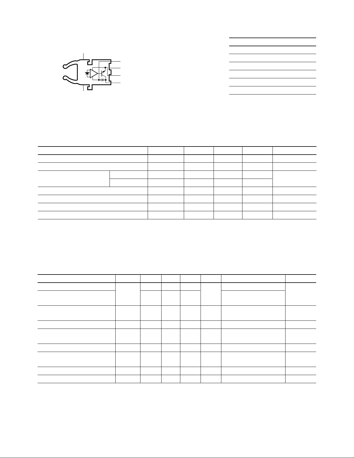
HFBR-25X3Z Receiver
DO NOT CONNECT 5
DO NOT CONNECT 8
4
3
2
1
V
CC
OPEN
GROUND
V
O
Pin # Function
1V
O
2 Ground
3 Open
4V
CC
5 Do not connect
8 Do not connect
Note: Pins 5 and 8 are for mounting and
retaining purposes only. Do not electrically
connect these pins.
Absolute Maximum Ratings
Parameter Symbol Min. Max. Units Reference
Storage Temperature T
Operating Temperature T
S
A
–40 +85 °C
–40 +85 °C
Lead Soldering Cycle Temp. 260 °C Note 1
Time 10 sec
Supply Voltage V
Average Output Collector Current I
Output Collector Power Dissipation P
Output Voltage V
Notes:
1. 1.6 mm below seating plane.
2. It is essential that a bypass capacitor 0.01 µF be connected from pin 2 to pin 3 of the receiver.
CC
O
OD
O
–0.5 7 V Note 2
–1 5 mA
25 mW
–0.5 7 V
Receiver Electrical/Optical Characteristics 0°C to 70°C, 4.5 V ≤VCC ≤5.5 V unless otherwise specified.
Parameter Symbol Min. Typ. Max. Units Conditions Ref.
Input Optical Power P
R(L)
–39 –13.7 dBm VO = VOL, IOL = 3.2 mA Notes 1,
Level Logic 0 –39 –13.3 VO = VOL, 2, 3
IOH = 8 mA, 25°C
Input Optical Power P
R(H)
–53 dBm VOH = 5.5 V Note 3
Level Logic 1 IOH = ≤40 µA
High Level Output Voltage V
Low Level Output Voltage V
High Level Supply Current I
Low Level Supply Current I
OH
OL
CCH
CCL
2.4 V IO = -40 µA, PR = 0 µW
0.4 V IOL = 3.2 mA Note 4
PR = P
R(L)MIN
1.2 1.9 mA VCC = 5.5 V, PR = 0 µW
2.9 3.7 mA VCC = 5.5 V, Note 4
PR = PRL (MIN)
Effective Diameter D 1 mm
Numerical Aperture NA 0.5
Notes:
1. Measured at the end of the fiber optic cable with large area detector.
2. Optical flux, P (dBm) = 10 Log P(µW)/1000 µW.
3. Because of the very high sensitivity of the HFBR-25X3Z, the digital output may switch in response to ambient light levels when a cable is not
occupying the receiver optical port. The designer should take care to filter out signals from this source if they pose a hazard to the system.
4. Including current in 3.3 k pull-up resistor.
18
Page 19

For product information and a complete list of distributors, please go to our website: www.avagotech.com
Avago, Avago Technologies, and the A logo are trademarks of Avago Technologies, Pte. in the United States and other countries.
Data subject to change. Copyright © 2006 Avago Technologies Pte. All rights reserved.
5989-4630EN February 3, 2006
 Loading...