

Page 1

PRELIMINARY HARDWARE DATA MODULE
BCM7405
General Information
5300 California Avenue • Irvine, CA 92617 • Phone: 949-926-5000 • Fax: 949-926-5203 06/29/07
2/24/2008 9T6WP
7405-1HDM00-R
Page 2

REVISION HISTORY
Revision # Date Change Description
7405-1HDM00-R 06/29/07 Preliminary release.
Broadcom Corporation
5300 California Avenue
Irvine, CA 92617
© 2007 by Broadcom Corporation
All rights reserved
Printed in the U.S.A.
®
Broadcom
Broadcom Corporation and/or its affiliates in the United States, certain other countries and/or the EU. Any other trademarks
or trade names mentioned are the property of their respective owners.
This hardware data module (including, without limitation, the Broadcom component(s) identified herein) is not designed,
intended, or certified for use in any military, nuclear, medical, mass transportation, aviation, navigations, pollution control,
hazardous substances management, or other high risk application. BROADCOM PROVIDES THIS HARDWARE DATA
MODULE "AS-IS", WITHOUT WARRANTY OF ANY KIND. BROADCOM DISCLAIMS ALL WARRANTIES, EXPRESSED
AND IMPLIED, INCLUDING, WITHOUT LIMITATION, THE IMPLIED WARRANTIES OF MERCHANTABILITY, FITNESS
FOR A PARTICULAR PURPOSE, AND NON-INFRINGEMENT.
, the pulse logo, Connecting everything®, and the Connecting everything logo are among the trademarks of
2/24/2008 9T6WP
Page 3

Preliminary Hardware Data Module BCM7405
06/29/07
TABLE OF CONTENTS
Document Overview.................................................................................................................................. 1-1
Overview .............................................................................................................................................. 1-2
Functional Description ............................................................................................................................. 1-3
Top-Level Overview ............................................................................................................................. 1-4
Features........................................................................................................................................ 1-5
Video Data Flow................................................................................................................................... 1-8
Overview ....................................................................................................................................... 1-8
Compressed Video Input .............................................................................................................. 1-8
Personal Video Recording ............................................................................................................ 1-9
Digital Video Decompression........................................................................................................ 1-9
ITU-R 656 Input ............................................................................................................................ 1-9
Video Processing .......................................................................................................................... 1-9
Video Encoder ............................................................................................................................ 1-10
Video DACs ................................................................................................................................ 1-10
Data Transport Processor .................................................................................................................. 1-11
Overview ..................................................................................................................................... 1-11
Features...................................................................................................................................... 1-11
Functional Overview ................................................................................................................... 1-13
Data Transport I/O Connections ................................................................................................. 1-16
Data Transport Input Bands
Throughput Data Rate
PID Parser
Packet Input Buffer
.......................................................................................................................... 1-17
............................................................................................................. 1-17
PID/Packet Substitution and Generation Module
Multistream CableCard Interface
Condition Access Descramblers (The Downstream Descramblers)
NDS ICAM Module
Copy Protection
PES Parser
......................................................................................................................... 1-21
.............................................................................................................. 1-20
.................................................................................................................. 1-20
PSI Section Filter and Processor
................................................................................................ 1-16
........................................................................................................ 1-16
................................................................ 1-18
........................................................................................ 1-19
................................... 1-20
........................................................................................ 1-21
Memory Buffer Manager
Interrupt Controller
Record Audio Video Engine (RAVE)
Document 7405-1HDM00-R Page iii
..................................................................................................... 1-22
.............................................................................................................. 1-22
................................................................................... 1-22
Broadcom Corporation
2/24/2008 9T6WP
Page 4

BCM7405 Preliminary Hardware Data Module
06/29/07
Audio/Video Interface
Playback
..............................................................................................................................1-25
Playback Sync Extractor
Remux Module
PCR Recovery Block
Serial STC Broadcast Module
..........................................................................................................1-25
.....................................................................................................1-26
....................................................................................................................1-26
...........................................................................................................1-27
.............................................................................................1-28
Broadcom Security Processor............................................................................................................1-28
Advanced Video Decoder ...................................................................................................................1-29
VC-1
....................................................................................................................................1-30
MPEG-2
MPEG-4 Part2
DivX
XVID
MPEG-1/H.261/H.263
...............................................................................................................................1-30
.....................................................................................................................1-30
.....................................................................................................................................1-30
....................................................................................................................................1-31
.........................................................................................................1-31
Features ......................................................................................................................................1-31
Supported Picture Sizes..............................................................................................................1-31
Output Data Format.....................................................................................................................1-31
AVD Block Diagram and Data Flow Description .........................................................................1-32
Advanced Audio Module.....................................................................................................................1-33
Features ......................................................................................................................................1-34
Overview of Audio Module ..........................................................................................................1-35
Video and Graphics Display ...............................................................................................................1-36
Overview .....................................................................................................................................1-36
Features
Video Subsystem
Graphics Subsystem
..............................................................................................................................1-36
................................................................................................................1-36
...........................................................................................................1-38
Top Level Partitioning..................................................................................................................1-38
Video (Broadcom Video Network) Subblock Description ............................................................1-39
AVC/MPEG-2/VC-1 Feeder
Video Feeder
Graphics Feeder
Video Scaler
.......................................................................................................................1-40
..................................................................................................................1-40
........................................................................................................................1-41
Motion Adaptive De-interlacer
Film Grain Technology
.................................................................................................1-40
.............................................................................................1-41
........................................................................................................1-42
Compositor
Page iv Document 7405-1HDM00-R
..........................................................................................................................1-42
Broadcom Corporation
2/24/2008 9T6WP
Page 5

Preliminary Hardware Data Module BCM7405
06/29/07
Capture Block
..................................................................................................................... 1-42
Digital Noise Reduction ............................................................................................................. 1-43
DNR Operations
.................................................................................................................. 1-43
Digital Contour Removal ............................................................................................................. 1-43
Graphics Subblock Description...................................................................................................1-44
Scaler Overview
Feeder Architecture (Source and Destination)
Color Keying and Color Matrix Architecture
Compositor Architecture
ROP Architecture
Capture Architecture
.................................................................................................................. 1-45
.................................................................... 1-46
........................................................................ 1-47
..................................................................................................... 1-48
................................................................................................................ 1-49
........................................................................................................... 1-49
Digital Video Decoder (ITU-R-656)............................................................................................. 1-50
VBI Decoding
...................................................................................................................... 1-50
Analog Video Encoder ................................................................................................................ 1-50
VBI Encoding
...................................................................................................................... 1-52
Video DACs ................................................................................................................................ 1-53
Digital Video Encoder ................................................................................................................. 1-53
Safe Mode
Supported Modes
Supported PC Scan Rates
........................................................................................................................... 1-53
................................................................................................................ 1-54
.................................................................................................. 1-55
RF Modulator ..................................................................................................................................... 1-56
Overview ..................................................................................................................................... 1-56
Features...................................................................................................................................... 1-56
Typical Usage Modes ................................................................................................................. 1-57
Supported Television Standards
Audio Transmission Modes
Baseband BTSC Composite Output Mode
Sound IF Output Mode
........................................................................................................ 1-58
Unsupported Audio Mode
......................................................................................... 1-57
................................................................................................. 1-58
......................................................................... 1-58
................................................................................................... 1-58
Memory Controller ............................................................................................................................. 1-59
Overview ..................................................................................................................................... 1-59
DRAM Physical Layer Controller ................................................................................................ 1-61
Memory Configurations Supported
..................................................................................... 1-61
DRAM Transaction Layer Controller........................................................................................... 1-62
Arbitration
Document 7405-1HDM00-R Page v
............................................................................................................................ 1-62
Broadcom Corporation
2/24/2008 9T6WP
Page 6

BCM7405 Preliminary Hardware Data Module
06/29/07
Buses
DDR-SDRAM Memory Image Organization
Digital Video Compression Standards
Memory Accesses for Video Decompression
..................................................................................................................................1-62
........................................................................1-62
.................................................................................1-62
......................................................................1-62
DDR Clock Generation ................................................................................................................1-62
MIPS4380 Processor Core.................................................................................................................1-63
Overview .....................................................................................................................................1-63
Architecture .................................................................................................................................1-63
Micro-Architecture .......................................................................................................................1-64
EJTAG Debug Support................................................................................................................1-64
Major Functional Blocks ..............................................................................................................1-65
Execution Unit
Multiply Divide Unit
Floating-Point Unit
.....................................................................................................................1-65
..............................................................................................................1-66
...............................................................................................................1-66
eDSP Extended Instructions .......................................................................................................1-67
MIPS16e Application-Specific Extension ....................................................................................1-67
Memory Management Unit with TLB ...........................................................................................1-67
System Control Coprocessor (CP0) ............................................................................................1-68
Instruction Cache ........................................................................................................................1-68
Data Cache .................................................................................................................................1-68
Level-Two Cache ........................................................................................................................1-69
Readahead Cache ......................................................................................................................1-69
Little and Big Endianness of Byte Ordering.................................................................................1-69
Debugging Support Unit ..............................................................................................................1-70
Peripherals .........................................................................................................................................1-71
Overview .....................................................................................................................................1-71
Peripheral Control Unit ................................................................................................................1-71
Keypad Controller........................................................................................................................1-71
LED Controller.............................................................................................................................1-71
IR Receiver Controller .................................................................................................................1-71
IR Blaster Controller ....................................................................................................................1-72
UHF Receiver..............................................................................................................................1-74
UART...........................................................................................................................................1-75
General Description
.............................................................................................................1-75
Functional Description
Page vi Document 7405-1HDM00-R
.........................................................................................................1-76
Broadcom Corporation
2/24/2008 9T6WP
Page 7

Preliminary Hardware Data Module BCM7405
06/29/07
Generic I/O Port Controller ......................................................................................................... 1-77
SPI Master .................................................................................................................................. 1-77
Programmable Queue
Wraparound Transfer Mode
Programmable Transfer Length
Programmable Transfer Delay
Programmable Queue Pointer
......................................................................................................... 1-78
................................................................................................ 1-78
.......................................................................................... 1-78
............................................................................................ 1-78
............................................................................................ 1-78
BSC Master ................................................................................................................................ 1-78
BSC Master Interface Operation
......................................................................................... 1-79
BSC Slave .................................................................................................................................. 1-79
BSC Operation
.................................................................................................................... 1-79
PWMs ......................................................................................................................................... 1-80
Timer/Counters ........................................................................................................................... 1-80
Smart Card Interfaces................................................................................................................. 1-80
Features
.............................................................................................................................. 1-81
M-Card CPU Interface ................................................................................................................ 1-82
Introduction
Input and Output Processes
......................................................................................................................... 1-82
............................................................................................... 1-83
PCI and External Bus Interface ..................................................................................................1-84
Advanced Connectivity Interface ................................................................................................ 1-89
Ethernet
Serial ATA Controller
USB
Soft Modem
PCI
.............................................................................................................................. 1-89
.......................................................................................................... 1-89
..................................................................................................................................... 1-90
......................................................................................................................... 1-91
...................................................................................................................................... 1-91
JTAG Interface............................................................................................................................ 1-91
Testability........................................................................................................................................... 1-92
Overview ..................................................................................................................................... 1-92
Production Testing ...................................................................................................................... 1-92
Scan
.................................................................................................................................... 1-92
Built-In Self-Test
................................................................................................................. 1-92
Functional Testing ...................................................................................................................... 1-92
Test Modes
Test Buses
......................................................................................................................... 1-92
.......................................................................................................................... 1-92
On-Board Testing ....................................................................................................................... 1-92
Broadcom Corporation
Document 7405-1HDM00-R Page vii
2/24/2008 9T6WP
Page 8

BCM7405 Preliminary Hardware Data Module
06/29/07
JTAG
...................................................................................................................................1-92
EJTAG
.................................................................................................................................1-92
Power Features ..................................................................................................................................1-93
Power Modes for DDR DRAM Memory Controller ......................................................................1-93
Power-Up Sequence ...................................................................................................................1-94
Hardware Signal Descriptions................................................................................................................1-95
Pin Definition Notations ......................................................................................................................1-96
Pin Labels....................................................................................................................................1-96
Pin Type ......................................................................................................................................1-96
Power-On Strap Settings..................................................................................................................1-147
Timing and AC Characteristics ............................................................................................................1-149
Data Transport Input Timing.............................................................................................................1-150
MPOD Input Timing ..........................................................................................................................1-151
Data Transport Output Timing..........................................................................................................1-152
RMX Serial Output Port Timing (Clock/Data/Sync Mode) .........................................................1-152
MPOD Output Timing .......................................................................................................................1-153
I2S Audio/Compressed I2S Output Timing.......................................................................................1-154
SPDIF Audio Output Timing .............................................................................................................1-155
DAC Audio Output Timing ................................................................................................................1-156
256Fs Audio Clock Output Timing....................................................................................................1-157
PCI Interface Timing.........................................................................................................................1-158
EBI Timing ........................................................................................................................................1-159
Asynchronous Read Transfer....................................................................................................1-159
Asynchronous Write Transfer....................................................................................................1-160
Synchronous Read Transfer .....................................................................................................1-161
Synchronous Write Transfer......................................................................................................1-162
DDR Interface Timing .......................................................................................................................1-163
HDMI and DVO.................................................................................................................................1-165
ITU656 Output Timing ......................................................................................................................1-166
Timing For ITU656 Output at vo_656 Pins ...............................................................................1-166
Timing For Alternate 656 Output at vi0_656 Pins .....................................................................1-167
Serial Teletext Port Output Timing ............................................................................................1-167
Timing For Serial Teletext Output at rmx_data1 Pin .................................................................1-167
Crystal Requirements............................................................................................................................1-168
Crystal Requirements .......................................................................................................................1-169
Broadcom Corporation
Page viii Document 7405-1HDM00-R
2/24/2008 9T6WP
Page 9

Preliminary Hardware Data Module BCM7405
06/29/07
3rd Overtone Crystal Oscillator.................................................................................................1-169
External Components ............................................................................................................... 1-170
SATA Crystal ............................................................................................................................ 1-170
Electrical Characteristics ..................................................................................................................... 1-171
Absolute Maximum Ratings ............................................................................................................. 1-172
Recommended Operating Conditions .............................................................................................. 1-172
Thermal Data ......................................................................................................................................... 1-173
Thermal Data ................................................................................................................................... 1-174
Mechanical Characteristics.................................................................................................................. 1-175
Mechanical Drawings ....................................................................................................................... 1-176
Ordering Information ............................................................................................................................ 1-179
Ordering Information ........................................................................................................................ 1-180
Broadcom Corporation
Document 7405-1HDM00-R Page ix
2/24/2008 9T6WP
Page 10

BCM7405 Preliminary Hardware Data Module
06/29/07
Broadcom Corporation
Page x Document 7405-1HDM00-R
2/24/2008 9T6WP
Page 11

Preliminary Hardware Data Module BCM7405
06/29/07
LIST OF FIGURES
Figure 1-1: Functional Block Diagram ............................................................................................................. 1-7
Figure 1-2: Video Data Flow Diagram ............................................................................................................. 1-8
Figure 1-3: Data Transport and Broadcom Security Processor Block Diagram ............................................ 1-14
Figure 1-4: Data Transport I/O Connections Diagram ................................................................................... 1-16
Figure 1-5: Advanced Video Decoding Module Block Diagram..................................................................... 1-32
Figure 1-6: Audio Block Diagram................................................................................................................... 1-33
Figure 1-7: Video and Graphics Block Diagram ............................................................................................ 1-38
Figure 1-8: Video Display Engine Block Diagram.......................................................................................... 1-39
Figure 1-9: DNR Position in BVN .................................................................................................................. 1-43
Figure 1-10: Memory-to-Memory Compositor Block Diagram ....................................................................... 1-45
Figure 1-11: Stripe Example.......................................................................................................................... 1-46
Figure 1-12: Color Keying Flow ..................................................................................................................... 1-48
Figure 1-13: VEC Block Diagram .................................................................................................................. 1-52
Figure 1-14: RF Modulator Block Diagram .................................................................................................... 1-56
Figure 1-15: Memory Controller Partition ...................................................................................................... 1-60
Figure 1-16: Block Diagram of the CPU ........................................................................................................ 1-65
Figure 1-17: Little and Big Endian Byte Ordering .......................................................................................... 1-69
Figure 1-18: Flash IR Scheme Example........................................................................................................ 1-72
Figure 1-19: IR Blaster Block Diagram .......................................................................................................... 1-72
Figure 1-20: Analog Front End of UHF Receiver with External Components................................................ 1-74
Figure 1-21: Digital Front End of UHF Receiver ............................................................................................ 1-75
Figure 1-22: UART Functional Block Diagram .............................................................................................. 1-76
Figure 1-23: Asynchronous Serial Data Waveform (01001011 Data, 8-bit Character, Even Parity) ............. 1-76
Figure 1-24: Variable-Frequency PWM Generation Diagram........................................................................ 1-80
Figure 1-25: Smart Card Interface Block Diagram ........................................................................................ 1-81
Figure 1-26: M-Card CPU Interface............................................................................................................... 1-82
Figure 1-27: MCIF Interfaces......................................................................................................................... 1-83
Figure 1-28: EBI Synchronous Read Cycle Between Two PCI Cycles ......................................................... 1-85
Figure 1-29: EBI Asynchronous Read Cycle Between Two PCI Cycles ....................................................... 1-86
Figure 1-30: EBI Asynchronous Write Cycle Between Two PCI Cycles........................................................ 1-87
Figure 1-31: EBI Synchronous Write Cycle Between Two PCI Cycles ......................................................... 1-88
Figure 1-32: SATA Core Block Diagram........................................................................................................ 1-90
Broadcom Corporation
Document 7405-1HDM00-R Page xi
2/24/2008 9T6WP
Page 12

BCM7405 Preliminary Hardware Data Module
06/29/07
Figure 1-33: Soft Modem Connections ..........................................................................................................1-91
Figure 1-34: Power-Up Sequence Waveforms Without On-chip Voltage Regulator......................................1-94
Figure 1-35: Data Transport Input Band Timing ..........................................................................................1-150
Figure 1-36: MPOD Input Timing .................................................................................................................1-151
Figure 1-37: RMX Serial Output Port Timing (Clock/Data/Sync Mode) .......................................................1-152
Figure 1-38: MPOD Output Timing ..............................................................................................................1-153
Figure 1-39: I2S Audio/Compressed I2S Output Timing Diagram ...............................................................1-154
Figure 1-40: SPDIF Audio Output Timing Diagram......................................................................................1-155
Figure 1-41: DAC Audio Output Timing Diagram.........................................................................................1-156
Figure 1-42: 256Fs Audio Clock Output Timing Diagram ............................................................................1-157
Figure 1-43: PCI Interface Timing Diagram .................................................................................................1-158
Figure 1-44: Async Read Timing Diagram ...................................................................................................1-159
Figure 1-45: Async Write Timing Diagram ...................................................................................................1-160
Figure 1-46: Synchronous Read Timing Diagram........................................................................................1-161
Figure 1-47: Synchronous Write Timing Diagram ........................................................................................1-162
Figure 1-48: Write Cycle Timing ..................................................................................................................1-163
Figure 1-49: Read Cycle Timing ..................................................................................................................1-163
Figure 1-50: Clock-to-Data Timing...............................................................................................................1-165
Figure 1-51: ITU656 Output Timing Diagram...............................................................................................1-166
Figure 1-52: Serial Teletext Port Output Timing Diagram ............................................................................1-167
Figure 1-53: Example: Vendor (TXC) Part Number for 3OT Crystal: 7EA0000023 .....................................1-170
Figure 1-54: 976-FCBGA+HS Package (With Heat Sink) ............................................................................1-176
Figure 1-55: 976-FCBGA+HS Package (Without Heat Sink).......................................................................1-177
Broadcom Corporation
Page xii Document 7405-1HDM00-R
2/24/2008 9T6WP
Page 13

Preliminary Hardware Data Module BCM7405
06/29/07
LIST OF TABLES
Table 1-1: Document Overview ....................................................................................................................... 1-2
Table 1-2: Video DAC Configuration ............................................................................................................. 1-10
Table 1-3: Definition of Terms ....................................................................................................................... 1-15
Table 1-4: Decode and Display Formats ....................................................................................................... 1-37
Table 1-5: Color and Alpha Selection............................................................................................................ 1-48
Table 1-6: Digital Video Decoder Supported Modes ..................................................................................... 1-50
Table 1-7: VBI Decoding ............................................................................................................................... 1-50
Table 1-8: Analog Video Encoder.................................................................................................................. 1-51
Table 1-9: VBI Encoding................................................................................................................................ 1-52
Table 1-10: DVI Supported Modes ................................................................................................................ 1-54
Table 1-11: ITU-656 Supported Modes ......................................................................................................... 1-54
Table 1-12: DVI PC Scan Clock Rates.......................................................................................................... 1-55
Table 1-13: PC Display Support .................................................................................................................... 1-55
Table 1-14: Supported Modulation Standards ............................................................................................... 1-57
Table 1-15: RFM Audio Usage Modes for Normal Operation........................................................................ 1-58
Table 1-16: FPU Latency and Repeat Rate .................................................................................................. 1-67
Table 1-17: Power Estimate .......................................................................................................................... 1-93
Table 1-18: Power Configuration Example.................................................................................................... 1-93
Table 1-19: Pin Descriptions ......................................................................................................................... 1-96
Table 1-20: Power-On Strap Settings.......................................................................................................... 1-147
Table 1-21: Data Transport Input Band Timing Parameters........................................................................ 1-150
Table 1-22: MPOD Input Timing Parameters .............................................................................................. 1-151
Table 1-23: RMX Serial Output Port Timing (Clock/Data/Sync Mode) Parameters .................................... 1-152
Table 1-24: MPOD Output Timing Parameters ........................................................................................... 1-153
Table 1-25: I2S Audio/Compressed I2S Output Timing Parameters........................................................... 1-154
Table 1-26: SPDIF Audio Output Timing Parameters ................................................................................. 1-155
Table 1-27: DAC Audio Output Timing Parameters .................................................................................... 1-156
Table 1-28: 256Fs Audio Clock Output Timing Parameters ........................................................................ 1-157
Table 1-29: PCI Interface Timing Parameters ............................................................................................. 1-158
Table 1-30: Async Read Timing Parameters............................................................................................... 1-159
Table 1-31: Async Write Timing Parameters ............................................................................................... 1-160
Table 1-32: Synchronous Read Timing Parameters ................................................................................... 1-161
Table 1-33: Synchronous Write Timing Parameters.................................................................................... 1-162
Broadcom Corporation
Document 7405-1HDM00-R Page xiii
2/24/2008 9T6WP
Page 14

BCM7405 Preliminary Hardware Data Module
06/29/07
Table 1-34: DDR Interface Timing Parameters............................................................................................1-164
Table 1-35: Nominal DVO Output Propagation Delays................................................................................1-165
Table 1-36: Timing for ITU656 Output at vo_656 Pins ................................................................................1-166
Table 1-37: Timing for Alternate 656 Output at vi0_656 Pins ......................................................................1-167
Table 1-38: Timing for Serial Teletext Output at rmx_data1 Pin..................................................................1-167
Table 1-39: Electrical Specifications ............................................................................................................1-169
Table 1-40: SATA Crystal Electrical Characteristics ....................................................................................1-170
Table 1-41: Absolute Maximum Ratings ......................................................................................................1-172
Table 1-42: Recommended Operating Conditions.......................................................................................1-172
Table 1-43: Thermal Data (Without External Heat Sink, 2s2p Board) .........................................................1-174
Table 1-44: Ordering Information.................................................................................................................1-180
Broadcom Corporation
Page xiv Document 7405-1HDM00-R
2/24/2008 9T6WP
Page 15

Preliminary Hardware Data Module BCM7405
06/29/07 Document Overview
General Information
DOCUMENT OVERVIEW
Overview ............................................................................................................................................ 1-2
Broadcom Corporation
Document 7405-1HDM00-R Page 1-1
2/24/2008 9T6WP
Page 16

BCM7405 Preliminary Hardware Data Module
Document Overview 06/29/07
OVERVIEW
The highlighted portion of Table 1-1 outlines information contained within the BCM7405.
Table 1-1: Document Overview
Document # Document Title Description
7405-1HDM0x General Information This document contains the following information:
• A Functional Description containing brief summaries of each functional
block contained within the BCM7405.
• Hardware Signal Descriptions
• Timing and AC Characteristics
• Electrical Characteristics
• Mechanical Drawing
• Ordering Information
7405-2HDM0x Front-End Functions The BCM7405 does not contain Front-End Functions
7405-3HDM0x Data Transport, Audio,
Video, and Graphics
7405-4HDM0x I/O Devices This document contains information on the following functionality:
7405-5HDM0x CPU Information This document contains information on the following functionality:
This document contains information on the following functionality:
• Data Transport Processor
• Advanced Audio Module
• Advanced Video Decoder
• Video and Graphics Display Module
• Broadcom Video Network (BVN) Components
• ITU656 Input
• Video Encoder Design
• High-Definition Multimedia Interface (HDMI)
• Memory-To-Memory Compositor
• RF Modulator
• Peripheral Module
• DDR-SDRAM Controller
• Memory Bus Architecture
• Shared EBI and PCI Bus
• Ethernet Controller and Interface
• Serial ATA 1.0 Host Controller
• Soft Modem Codec Interface
• Universal Serial Bus (USB) Host Interface
• Test BSC Slave Interface
• MIPS32™ CPU Core
Broadcom Corporation
Page 1-2 Overview Document 7405-1HDM00-R
2/24/2008 9T6WP
Page 17

Preliminary Hardware Data Module BCM7405
06/29/07 Functional Description
General Information
FUNCTIONAL DESCRIPTION
Top-Level Overview ........................................................................................................................... 1-4
Video Data Flow................................................................................................................................. 1-8
Data Transport Processor ................................................................................................................ 1-11
Broadcom Security Processor.......................................................................................................... 1-28
Advanced Video Decoder................................................................................................................. 1-29
Advanced Audio Module .................................................................................................................. 1-33
Video and Graphics Display ............................................................................................................. 1-36
RF Modulator.................................................................................................................................... 1-56
Memory Controller............................................................................................................................ 1-59
MIPS4380 Processor Core............................................................................................................... 1-63
Peripherals ....................................................................................................................................... 1-71
Testability ......................................................................................................................................... 1-92
Power Features ................................................................................................................................ 1-93
Broadcom Corporation
Document 7405-1HDM00-R Page 1-3
2/24/2008 9T6WP
Page 18

BCM7405 Preliminary Hardware Data Module
Functional Description 06/29/07
TOP-LEVEL OVERVIEW
The BCM7405 is a next-generation high-definition satellite, cable, and IP set-top box solution offering integrated AVC
(H.264/MPEG-4 Part 10), MPEG-4 Part 2, MPEG-2, and VC-1 video decoding technology. It also supports DivX, H.263, and
XviD formats. The BCM7405 combines a data transport processor, high-definition video decoder, advanced-audio decoder,
2D graphics processing, high-quality video scaling and motion adaptive de-interlacing, six video DACs, stereo high-fidelity
audio DACs, a MIPS 4380 class processor with FPU, and a peripheral control unit providing a variety of set-top box control
functions.
The Data Transport Processor is an MPEG-2 DVB-compliant transport stream message/PES parser and demultiplexer. It is
capable of simultaneously processing 255 PIDs via 128 PID channels in up to six independent external transport stream
inputs and five internal playback channels. The data transport supports decryption for up to 128 PID channels in all streams.
All 128 PID channels can be used by the Record, Audio, and Video interface engine (RAVE), PCR processors, message
filter as well as for output via the high-speed transport or remux module. The data transport module RAVE supports 24
channels. Each RAVE channel can be configured as either a record channel for PVR functionality or as an AV channel to
interface to audio and video decoders. The transport provides 1DES/3DES/DVB/Multi2/AES descrambling support.
memory-to-memory DMA security module may be programmed for supporting AES/1DES/3DES/CSS/CPRM/CPPM/DTCP
copy protection algorithms/standards.
The BCM7405 features an enhanced Broadcom Secure Processor providing secure boot key generation, management, and
protection.
A
An advanced video decoder is featured in the BCM7405, capable of supporting high-definition AVC, VC-1, and ATSC
MPEG-2 streams. AVC support is up to High Profile Level 4.1. New tools in the AVC Fidelity Range extensions are
supported, including 8x8 transform and spatial prediction modes, and adaptive quantization matrix. The video decoder also
supports high-definition VC-1 (Advanced Profile Level 3, Main, and Simple Profiles) and ATSC compliant MPEG-2, Main
Profile at Main and High Levels. The BCM7405 has an advanced programmable audio processor capable of decoding a
broad range of formats including Dolby Digital, Dolby Digital Plus, AAC 5.1, AAC+ Level 2, AAC+ Level 4, WMA, and MPEG
1 Layer 1, 2, and 3 with simultaneous pass-through support. 3D SRS Audio is also supported. The audio processor also
supports advanced transcoding to DTS as an example. Available audio outputs are an SPDIF and one pair of analog outputs.
High-quality video and graphics processing are integrated into the chip, featuring advanced studio quality 2D graphics
processing while still maintaining efficient use of memory bandwidth. Also included are motion adaptive de-interlacing with
3:2 pull-down, and Letterbox Detection. Digital Noise Reduction support is also included; this reduces mosquito noise and
MPEG artifacts, including block noise. Digital contour removal is also supported for low bit rate AVC streams.
The BCM7405 has a dual-stream analog video encoder with Macrovision™ that supports the following output standards:
NTSC-M, NTSC-J, PAL-BDGHIN, PAL-M, PAL-Nc, and SECAM. The following output formats are supported: composite, Svideo, SCART1, SCART2, RGB and YPrPb component. The following output resolutions are supported: 480i, 480p, 576i,
576p, 720p, and 1080i. Six output DACs are available to be shared amongst the output functions. The BCM7405 also
supports output over an HDMI interface and a Channel 3/4 RF Modulator. An ITU-R-656 output port with Teletext sideband
is available if an interface to an additional external video encoder is desired. A high-definition digital video output port is also
available.
The BCM7405 incorporates a complete R4000 family FPU-based microprocessor subsystem, including caches with bridging
to memory and a local bus. NAND and NOR flash is supported. Integrated peripherals include three UARTS, two ISO7816
smart card interfaces, counter/timers, GPIO, LED/keypad controller, IR receivers, IR blaster, UHF remote control receiver,
an integrated soft modem system side device, and BSC and SPI controllers. Advanced connectivity features include two
USB 2.0/1.1 ports, an additional independent USB 2.0/1.1 port, a serial ATA port, an Ethernet port with MAC with an
integrated PHY and a dedicated Media Independent Interface (MII).
Broadcom Corporation
Page 1-4 Top-Level Overview Document 7405-1HDM00-R
2/24/2008 9T6WP
Page 19

Preliminary Hardware Data Module BCM7405
06/29/07 Functional Description
The Macrovision enabled version of this device may only be sold or distributed to authorized Macrovision buyers. If you have
a Macrovision enabled device, then the following applies:
This device is protected by U.S. patent numbers 4,631,603,4,577,216 and 4,819,098 and other intellectual property
rights. The use of Macrovision's copy protection technology in the device must be authorized by Macrovision and is
intended for home and other limited pay-per-view uses only, unless otherwise authorized in writing by Macrovision.
Reverse engineering or disassembly is prohibited.
FEATURES
• Advanced AVC/MPEG-2/VC-1 video decoder supporting the following:
- High profile up to level 4.1 H.264/AVC streams (up to Mbps) at 30 frames/sec.
- High or main profile level 3.1 H.264/AVC streams at 60 frames/sec
- New tools in the AVC fidelity range extensions
• 8 x 8 transform and spatial prediction modes
• Adaptive quantization matrix
• DivX 3.11, 4.1, 5.x progressive and interlaced
- VC-1 advanced profile @ level 3
- VC-1 simple and main profile
- HD MPEG-2 4:2:0 streams (up to 125 Mbps) at 30 frames/sec
- SD MPEG-2 4:2:0 streams at 60 frames/sec
- Still picture decode
- HD +SD simultaneous decode
- MPEG4 P2 SP/ASP L5 SD Progressive/Interlaced
• Advanced Audio Processor supporting decode of the following formats:
- AAC LC, AAC LC+SBR Level 2, AAC+ Level 2, AAC+ Level 4
- Dolby Digital, Dolby Digital Plus
- MPEG I Layer 1, 2
- MPEG I Layer 3 (MP3)
- Windows Media Audio (WMA)
-WMA pro
- AAC HE 5.1 decode plus DTS 5.1 encode SPDIF output
- AAC HE 5.1 decode plus AC3 5.1 encode SPDIF output
- MP3 encoding
• One pair of stereo high-fidelity audio DAC
• 3D SRS Audio Support
2
• One I
• One I
• One SPDIF output
• Advanced 2D-effects graphic engines
• Digital Noise Reduction (DNR)
• Digital Contour Removal
S input port
2
S output port
- Studio quality text and graphics at HD resolution
- Supports multiple layers and windows
- Reduces MPEG artifacts including block noise reduction
- Reduces mosquito noise
Broadcom Corporation
Document 7405-1HDM00-R Top-Level Overview Page 1-5
2/24/2008 9T6WP
Page 20

BCM7405 Preliminary Hardware Data Module
Functional Description 06/29/07
- Removes banding effects in low bit rate video applications
• Motion adaptive de-interlacer (MAD) with reverse 3:2/2:2 pull-down
• Letter box detection
• ITU-R-656 Digital input. Film grain technology.
• Video encoder
- Supports one SD/HD video stream
- Additionally supports one SD video stream scaled down from the HD content or independent SD.
- NTSC-M, NTSC-J, PAL-BDGHIN, PAL-M, PAL-Nc, SECAM Analog Outputs
- 480i/480p/576i/576p/720p/1080i output formats
- Component RGB or YPrPb Output
- Macrovision 7.1 Support
- Euro-SCART
- Displays component, S-video, and composite via six on-chip DACs
• HDMI/DVI with HDCP 1.2
• ITU-R-656 and 12-bit double clocked 24 bpp HD DVO Outputs
• Next generation Broadcom Security Processor supporting external codes and keys
• AES/1DES/3DES/CPRM/CPPM/CSS/DTCP copy protection algorithms/standards
• DVB, ARIB, and DC2-compliant transport demux with 1DES/3DES/DVB/Multi2/AES descramblers
• V.92 capable soft modem with:
- Integrated SiLab Si305X System Side Device
- Optional five-wire external interface
• 33 MHz PCI 2.3 with 5 volt tolerance
• On chip VCXOs
• Two DDR DRAM controllers
- Primary 64-/32-bit DDR controller
- Optional 32-/16-bit DDR controller
• Dual USB 2.0 host controller with dual port integrated transceiver
- Additional USB 2.0/1.1 host/client controller independent from the dual USB 2.0 controller
• Dual serial ATA-II interface
- SATA ports support hot plug and external SATA drives
• MIPS 4380 class processor with FPU
• RF Modulator with BTSC encoder
• Dual Ethernet
- First MAC to connect to internal integrated 10/100 BASE-T PHY
- Second MAC to connect to MII interface
The BCM7405 incorporates a complete MIPS 4380 Floating Point CPU microprocessor subsystem. including with bridging
to memory and a local bus, where external peripherals can be attached. Integrated peripherals include the following:
• Three UARTS
• UARTC is 16550 compatible
• Two ISO7816 smart card interfaces
• Counter/timers
• GPIO
• LED/keypad controller
Broadcom Corporation
Page 1-6 Top-Level Overview Document 7405-1HDM00-R
2/24/2008 9T6WP
Page 21
Preliminary Hardware Data Module BCM7405
06/29/07 Functional Description
• Two IR receivers
• IR blaster
• UHF remote control receiver
• BSC and SPI controllers
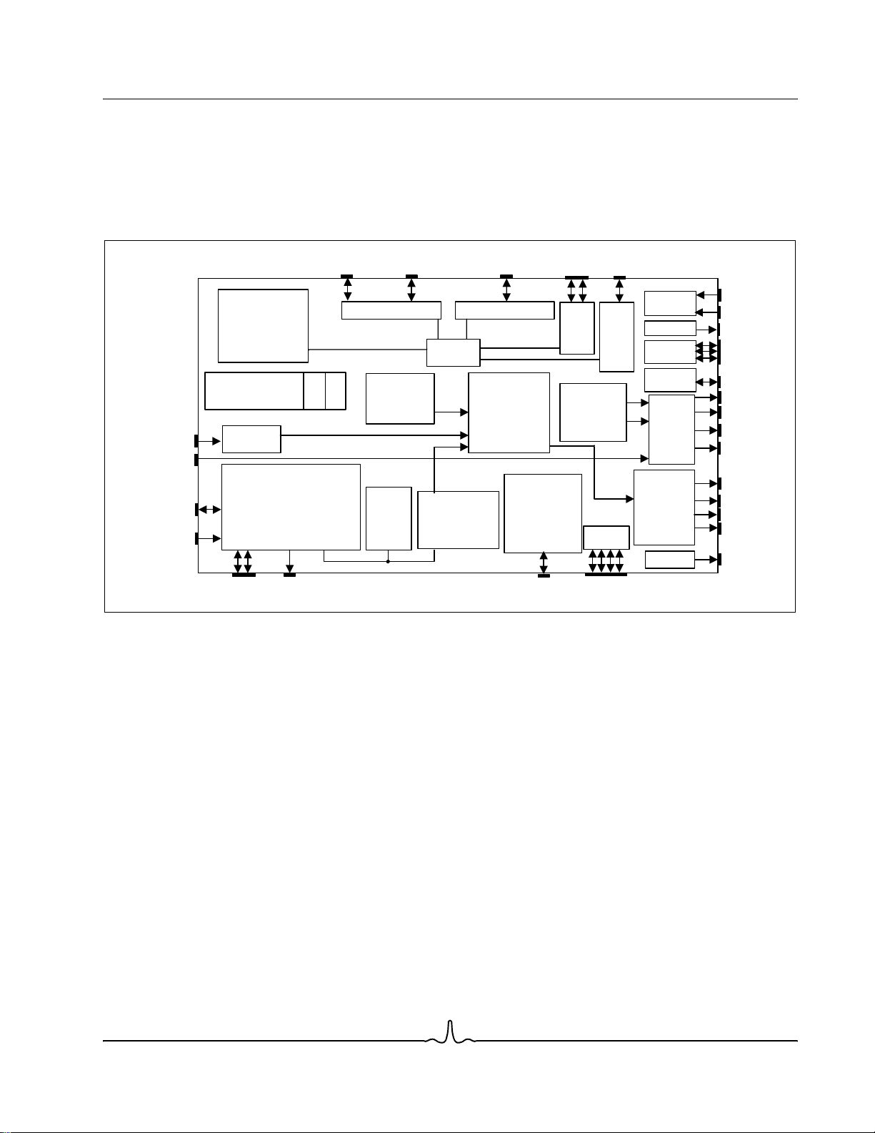
Figure 1-1 on page 1-7 shows the BCM7405 functional block diagram.
ITU-R-656
2
S In
I
MCARD/
SCARD
Transport Input x6
PCI 2.3 and Flash
400 MHz
MIPS32/16e
32KI and 64KD
MMU and FPU
8K RAC
128K L2
Secur e Pr ocessor
ITU-R-656
Decoder
MPEG-2/DVB Transport with
Descrambling and Conditional
Access Support
ISO7816 I/F
x2
R
O
M
RMX
x2
DMA
Configurable
64-bit DDR2
Video
-Scalers
- Compositors
- Digital noise
reduction
- Delinterlacing
Soft Modem,
Si305X,
Ethernet
10/100
BASE-T
nd
Enet MAC
2
Gateway
Services
USB 2.0 x2
Dual Serial
ATA-2
Bus Bridge DRAM Controller
O
T
P
Advanced
2D Graphics
Display
Engine
Dual
PVR
Engine
w/T r ick
Modes
High definition
AVC/MPEG-2//
MPEG-4/VC-1
Video Decoder
Figure 1-1: Functional Block Diagram
Dual
USB
2.0
Multiformat
Audio
Decoder
BSC
BSC x4
USB 2.0
Host/Client
USB
2.0
Composite
NTSC/PAL
IR/UHF
RX
IR TX
Tr iple
UARTs
GPIO
PCM
Audio
Engine
and
DACs
Dual
VEC with
six DACs
RF Mod.
IR In x2
UHF In
IR Out
UARTx3
GPIO
L
R
SPDIF
I2S Out
HD/SD Video
SD Video
ITU-R-656/TTX
HDMI
Channel 3/4
Broadcom Corporation
Document 7405-1HDM00-R Top-Level Overview Page 1-7
2/24/2008 9T6WP
Page 22
BCM7405 Preliminary Hardware Data Module
Functional Description 06/29/07
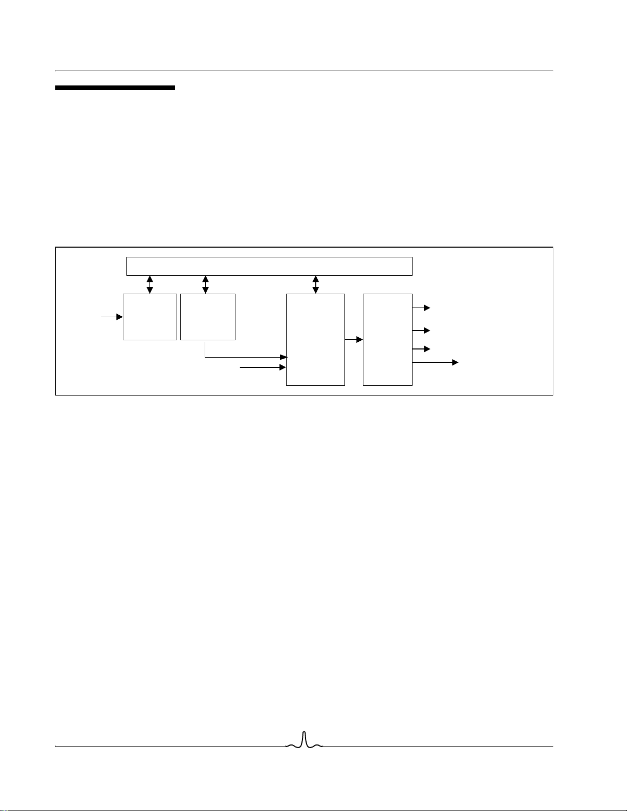
VIDEO DATA FLOW
OVERVIEW
At the top level, video signals flow through the video portion of the BCM7405 as compressed digital data or digitized
baseband analog video. From the appropriate decoder (AVC/MPEG-2/VC-1 decompression or ITU-R-656 video decoding),
the video data passes to the video processing stage where any scaling can be applied and the resulting video can be stored
to memory for later display. During this video processing, any graphics or additional video can be combined just before being
displayed. The manipulated video is then sent to the VEC(s) for display through either the analog DAC outputs, the ITU-R656 output, and/or through the HDMI interface. Figure 1-2 illustrates this high-level data flow.
DRAM Memory
Data
Transport
Processing
AVC/MPEG-2/
VC-1 Video
Decoder
ITU-R-656
Video
Processing
(Scaling,
Capture,
Compositing)
Video
Encoder(s)
Six Video DACs
HDMI output
HD DVO output
ITU-R-656
Figure 1-2: Video Data Flow Diagram
COMPRESSED VIDEO INPUT
Compressed video data normally enters the device in the form of MPEG transport streams. These come through the Data
transport that parses the stream and performs preprocessing. Video can also be stored directly into DRAM via local or
network peripherals—such as the HDD (for PVR), home networking (Ethernet) and so on.
The data transport is responsible for the following functions:
• Error detection in the video stream
• Locking the time base to PCR/SCR embedded within the stream
• Extracting PTS and DTS timestamps
• Extraction of start codes (and building index tables for these codes)
A detailed description of the data transport is provided in “Data Transport Processor” on page 1-11.
Broadcom Corporation
Page 1-8 Video Data Flow Document 7405-1HDM00-R
2/24/2008 9T6WP
Page 23

Preliminary Hardware Data Module BCM7405
06/29/07 Functional Description
PERSONAL VIDEO RECORDING
Processing of compressed streams for Personal Video Recording (PVR) extends the normal processing by adding a number
of capabilities. In recording for PVR, the transport packets associated with the program selected are recorded to a circular
buffer in DRAM for transfer to the hard disk drive (HDD). The compressed data is optionally scrambled using the mem-tomem security block. In addition, the video elementary stream (ES) data contained within the selected PID is searched for
the presence and location of selected start codes, such as PES packet headers, sequence start codes, picture start codes,
and the first slice start codes within each picture. Sufficient data from the compressed streams following the start codes is
also retained to determine the picture type (I, B, or P) and other pertinent information. All of this selected information is written
to memory in a circular buffer to facilitate additional processing by the Host MIPS as required, and to record the data to the
HDD. The PES packets can be recorded as an alternative to Transport streams.
In PVR playback, the transport processor reads linked lists of compressed audio and video from DRAM, optionally
descrambling it using mem-to-mem security block, and processes it for decompression and display in a manner that is similar
in many ways to normal (non-stored) decoding. The PVR playback supports special capabilities for fast and slow decoding
and descrambling, and data flow management in the absence of a physical time base associated with the stream (as would
normally be present in broadcast operation).
DIGITAL VIDEO DECOMPRESSION
Decompression of digital video is performed by the AVC/MPEG-2/VC-1 processor. The decoder extracts compressed video
and index tables from DRAM (created by the data transport). The video is decoded or decompressed and the resultant is
stored back into DRAM in picture (frame or field) buffers in YCrCb 4:2:0 format. The decoder needs multiple picture buffers
to account for differing time bases and decode rates.
ITU-R 656 INPUT
The BCM7405 supports an ITU-R 656 video input. The input has a dedicated VBI decoder to handle Teletext, NABTS, Close
Caption, CGMS-A, Gemstar, and WSS.
VIDEO PROCESSING
The display engine takes in uncompressed video from either the AVC/MPEG-2/VC-1 decoder or the digital ITU-R-656 input.
The display engine can scale the video in horizontal and vertical directions and either display the video immediately (in-line)
or capture it to memory for later viewing. Scaling is optional, and may be needed for normal display of digital or analog video.
The scaling function incorporates a format conversion capability for converting between various standard definition (SD) and
HD formats of video signals and those required by the displays. Capture of video to memory is used either when it is
advisable to minimize peak DRAM bandwidth requirements, or when it is unavoidable due to the constraints of the video
input and output timing. In general, capturing to memory when scaling reduces peak DRAM bandwidth when the scale factor
is less than 1.0. The video and graphics processing is further expanded in “Video and Graphics Display” on page 1-36.
Broadcom Corporation
Document 7405-1HDM00-R Video Data Flow Page 1-9
2/24/2008 9T6WP
Page 24

BCM7405 Preliminary Hardware Data Module
Functional Description 06/29/07
VIDEO ENCODER
The VEC supports a variety of analog video standards (NTSC [all variations], PAL [all variations], SECAM, 480i, 480p, 576i,
576p, 720p, 1080i, 1080p24, and 1080p30) as well as HDMI digital video standards. 1080p50 and 1080p60 display formats
are not supported.
Each VEC also receives encoded VBI signals from associated VBI encoders. The VBI data combines with the appropriate
lines of video. This arrangement supports Closed Caption, NABTS, Teletext, CGMS-A, Gemstar, SCTE20/21, AMOL I/II,
analog pass-through, and other VBI formats on the CVBS and Y/C outputs.
The VEC outputs either an HD or SD stream on the first television output, and a scaled down version of an HD image on the
second television output. The BCM7405 provides a single user experience that allows for simultaneous outputs of the same
content for high definition and standard definition televisions.
VIDEO DACS
The BCM7405 integrates a set of six 10-bit video DACs, using Broadcom’s proven high-speed CMOS DAC technology.
These DACs are configured to support SCART1 as well as component, S-Video (Y/C), and composite video (CVBS) outputs.
Table 1-2 outlines the configuration parameters.
Table 1-2: Video DAC Configuration
Usage Mode Video Display 1 Video Display 2
Unless otherwise noted, each box indicates the analog format that is provided for the indicated usage mode. Each display
has its own graphics compositor, which can be independently controlled.
3:3 Configuration Component (including 480P RGB) Composite and S-Video of the same
content as video display 1.
4:2 Configuration Component (including 480P RGB) + Composite Composite or S-Video of the same
content as video display 1.
Broadcom Corporation
Page 1-10 Video Data Flow Document 7405-1HDM00-R
2/24/2008 9T6WP
Page 25

Preliminary Hardware Data Module BCM7405
06/29/07 Functional Description
DATA TRANSPORT PROCESSOR
OVERVIEW
The data transport processor is an MPEG-2/DIRECTV transport stream message/PES parser and demultiplexer. It can
simultaneously process 255 PID filters via 255 PID channels in up to six independent external transport stream inputs and
five internal playback channels, with decryption for all 255 PID channels. It supports message/PES parsing for 128 PID
channels with storage to 128 external DRAM buffers, and it provides 512 4-byte generic section filters that can be cascaded
to provide effectively longer filters (up to 64-bytes or 128 filters of 16-bytes each). The data transport module provides two
sets of a two-channel remux output. The data transport module has a RAVE (record, audio, and video interface engine)
function, which can be configured to support 24 channels. Each RAVE channel can be configured as record channel for PVR
functionality or as an AV channel to interface audio and video decoders.
FEATURES
• Capable of processing six independent external transport stream inputs and five internal playback channels
simultaneously.
• MPEG and DIRECTV transport streams can be processed concurrently.
• Supports ARIB.
• Supports TSMF as defined by Japan Cable Television Engineering Association spec JCTEA STC-007-2.
• Maximum input band transport stream rate supported is 100 Mbps.
• Maximum combined transport stream burst rate can be greater than 216 Mbps based on usage.
• Maximum combined transport stream average rate after PID filtering is 216 Mbps.
• Supports 255 PID filters via 255 PID channels.
• Supports a 255-entry Primary PID table for parsing MPEG transport packets. Primary PID table entries can be
arbitrarily assigned to any of the parser bands. The parser bands are processed uniquely, even in cases when they use
the same PID.
• Supports a 255-entry Secondary PID table for parsing MPEG transport packets. Each entry in Secondary PID table is
associated with PID table entry and packets with primary or secondary PID can be mapped to same PID channel for
PID merge function.
• Mode to store complete transport packet in the external DRAM message buffers.
• PES packet extraction for up to 128 PID channels.
• PSI section extraction for up to 128 PID channels with filtering.
• Only PID channels 0-127 are routed to Message filer.
• Supports 512 generic filters capable of filtering up to 4 bytes each for PID channels 0-127. These filters can be
cascaded to provide effectively longer filters (up to 64-bytes).
• Each generic filter includes a 4-byte inclusion mask and a 4-byte exclusion mask for independent inclusion and
exclusion per bit filtering.
• Generic filters are divided into 16 banks, each with 32 4-byte filters. Banks of 4-byte filters can be cascaded to make up
groups of filters that are effectively up to 64 bytes wide. Each PID channel can independently select one group of filters.
Each PID channel can use any number up to 32 filters in that group. Each PID channel can independently select its own
programmable generic filter offset.
• Includes a special addressing mode for filtering of MPEG and Private stream messages for PID channels 0-127.
• The special addressing mode filter and the generic section filters can be enabled simultaneously for each PID channel.
• Data extracted from the parser bands is stored in one or more of the 128 message buffers and/or using RAVE (record,
audio and video interface engine) in the external system DRAM.
• Supports 10 external DRAM message buffer sizes: 1K, 2K, 4K, 8K, 16K, 32K, 64K, 128K, 256K, and 512K bytes.
Broadcom Corporation
Document 7405-1HDM00-R Data Transport Processor Page 1-11
2/24/2008 9T6WP
Page 26

BCM7405 Preliminary Hardware Data Module
Functional Description 06/29/07
• Each message buffer is associated with a PID channel.
• Section filter supports the capability to overwrite the CRC of a valid MPEG PSI message with a fixed pattern or with the
section filter match tag, or append of filter match tag to each saved message.
• Error handling of messages.
• Messages written into the message buffer are optionally 32-bit word aligned. Message length is unchanged.
• Supports 24 RAVE channels. Each RAVE channel can be configured as a record channel for PVR or as an AV channel
to interface to audio and video decoders.
• Each record channel can record up to 128 PID channels from a transport stream.
• Supports up to six transport parser index tables for use in PVR applications.
• Supports up to 32 SCDs (Start Code Detect Table). One SCD is required for each AV channel and up to eight SCDs
can be assigned to each record channel for Start Code Detect Index Table.
• Supports parsing of Transport/PES data to ES and generate CDB/ ITBs for audio/video decoders.
• Five independent playback channels to provide data to the video, audio and/or two remux modules.
• Supports data transport local timestamp insertion for record and playback of transport streams.
• PID filter, Packet Substitution, and PCR correction support for two dual-channel remux Interface blocks with a maximum
100 Mbps rate. Combines any two transport streams from the available input streams or playback channels.
• Supports four independent PCR recovery blocks.
• Most of the programmable control registers are readable by the host MIPs.
• Support glue-less M-card and S-card interface from MPOD block in transport design
• PCROFFSET block to support Mosaic mode, i.e., support of 16 PCR PIDs and all audio/video PID channel can map to
any PCR PID, irrespective of Parser band
• Packet substitution for six band support
• Support per context picture counter in RAVE
• Support separate ITB indication for garbage data in RAVE
• Support mechanism to extract up to 8 bytes of data after start code in RAVE ITB
• Support DLNA timestamp format in record path
• Support DLNA timestamp format in playback path
• Includes Broadcom Security Processor with OTP for key generation.
• Security features:
- Supports Passage as defined by Sony
- Supports Multi-Stream CableCard as defined by OpenCable Advanced Multi-Stream POD (MPOD) Interface
Specification
- Supports RASP as defined by NDS
- Supports an NDS ICAM 2.2 Module
- 1DES/3DESDVB/Multi2/AES Descrambler for Conditional Access for up to 128 PID channels. Supports either 64-bit
or 56-bit DES keys. Supports 128 bit AES and 3DES keys. Support 64-bit Multi2 keys and four 256-bit system keys.
- Mem-to-Mem DMA Security module for AES, 1DES, 3DES, C2 (CPRM, CPPM), CSS, M6 for Copy Protection.
Supports 42 keys which can be configured as 64-, 128-, or 192-bit keys.
Broadcom Corporation
Page 1-12 Data Transport Processor Document 7405-1HDM00-R
2/24/2008 9T6WP
Page 27

Preliminary Hardware Data Module BCM7405
06/29/07 Functional Description
FUNCTIONAL OVERVIEW
The Data Transport Processor is an MPEG-2/DIRECTV transport stream message/PES parser and demultiplexer. It is
capable of simultaneously processing 255 PIDs via 255 PID channels in up to six independent transport streams using the
six available parsers. These six streams are selected from six external serial transport stream inputs, and five internal
playback channels. The data transport supports decryption for up to 128 PID channels in the six streams. All 128 PID
channels can be used by RAVE, PCR processors, message filter as well as for output via the high-speed transport or remux
module.
The data transport supports up to 128 PID channels for message or generic PES processing and storage in up to 128
external DRAM message buffers. There are 512 4-byte generic filters supported for processing of MPEG/DVB sections or
DIRECTV messages. A special addressing mode filter is included for up to 32 PID channels (PID channels 0-31), which
filters MPEG and private stream messages.
The data transport module supports RAVE (record, audio, and video interface engine) function, which supports up to 24
channels. Each RAVE channel can be configured as a record channel for PVR or as an AV channel to interface to audio and
video decoders. The RAVE supports up to a total of 32 SCDs (configured 0-8 per record channel).
The data transport also provides four PCR recovery blocks and two serial STC broadcast block for transmitting the STC to
the decoders.
The Broadcom data transport processor, shown in Figure 1-3, is an MPEG-2/DIRECTV transport stream message/PES
parser and demultiplexer. The module is capable of simultaneously processing 255 PIDs via 255 PID channels in up to six
independent transport streams, which are selected from six serial transport stream inputs and five internal playback
channels. The processor supports decryption for up to 128 PID channels. The processor supports up to 128 PID channels
for message or generic PES processing for storage in external message buffers. All 128 PID channels can be used for RAVE
(record, audio and video interface engine), PCR processors as well as for output via the high speed transport or remux
module. 512 4-byte generic filters are supported for processing of MPEG or DVB sections. It includes a special addressing
mode that filters MPEG and private stream messages. It provides 128 message buffers that reside in external memory that
can be used to store the messages from the 128 PID channels.
Broadcom Corporation
Document 7405-1HDM00-R Data Transport Processor Page 1-13
2/24/2008 9T6WP
Page 28
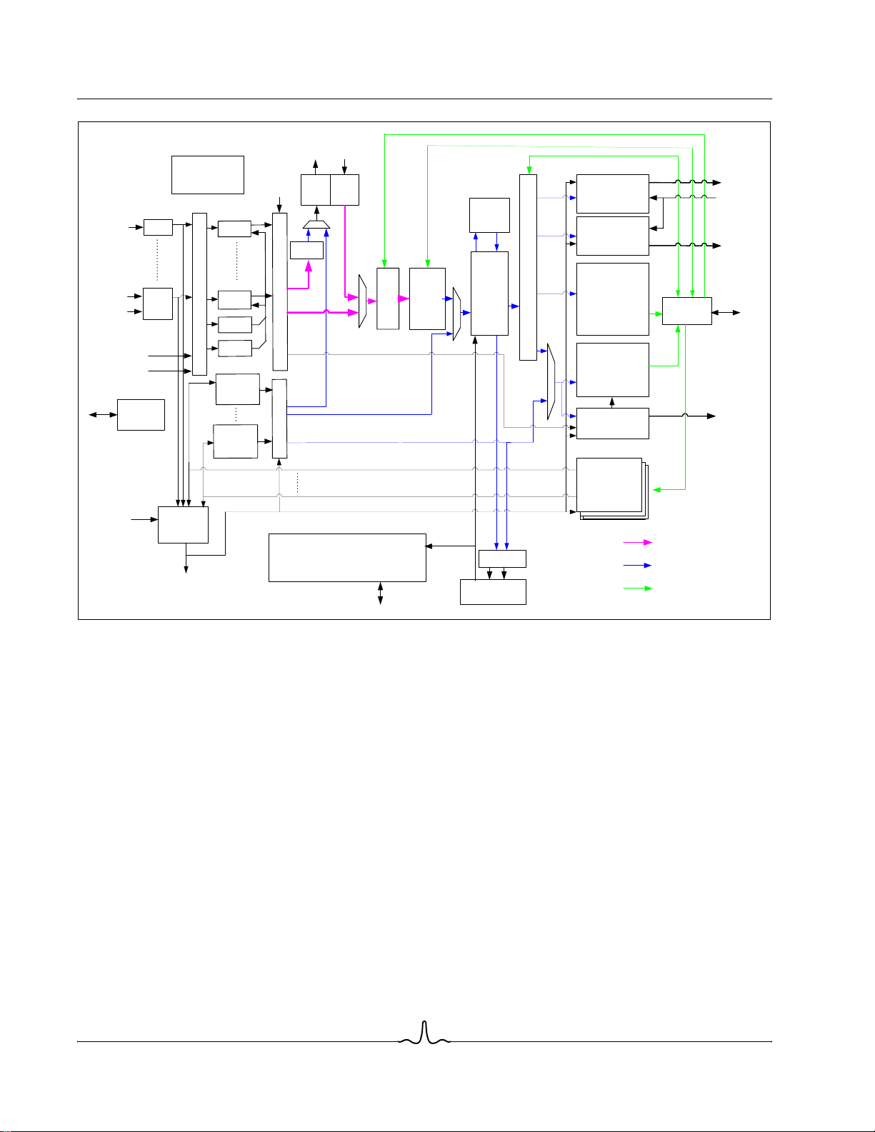
BCM7405 Preliminary Hardware Data Module
Functional Description 06/29/07
To
From
MPOD
MPOD
MPOD
MPOD
Out
In
32 bit to
8 bit
Pkt Sub
DMA
link-
list
T
i
m
e
s
t
a
m
p
Timebase for Timestamp restamp
n# Playback Transport, PES or ES
Mem -to-Mem Security
AES , 1 DES, 3DES, C 2 ( CPRM, CPPM),
CSS, DTCP + Key table
Mem-to-Mem
I/F-0
RS
Buffer
(DRAM
Interface)
NDS ICAM
Module
1DES/
DVB/AES/
Multi2
Descram-
bler
+
Key table
(216
Mbps)
ICAM -3
Monitor
BSP
(not in Transport)
X
C
B
U
F
F
E
R
(
D
R
A
M
)
Timebase
REMUX
2 Channel with PCR
correction, PID map
REMUX
2 Channel with PCR
correction, PID map
MPEG/ DIRECTV
128 PES Parser
+
Message filter
512 filters
4-bytes each
+ 128 DMA
buffers
RAVE
ITB + CDB
24 channels (each
channel configured as
either Record or AV),
33 SCD and 5 TPIT
PCROFFSET
Playback 0 to n
Link-list , pacing
XPT_XMEMIF
STC Broadcast
(To audio /video
decoders)
32 bit xpacket ibus
8 bit xpacket ibus
XMEM interface
RMX0
clocks
(ib0-n, 10 8, 81,
54,40.5,27,
20.25)
RMX1/
RMX1P
SCB
IB0
Transport Stream
Inputs
IB5
IB5P
RMX0 feedback
RMX1 feedback
GISB
GISB 2RBUS
EXT Inputs
Sync
Sync
PCR Timebase
Timebas e
pulses
255 Primary PID +
(255 Secondary PID
Table with Passage)
+ CC table
a
P
D
A
T
A
P
M
U
X
T
T
B
P
a
P
p
B
P
a
P
# x
S
S
c
r
a
#
c
a
s
e
r
s
m
M
M
p
a
+
k
e
r
s
+
k
e
0
r
e
r
F
0
1
F
e
r
r
s
t
i
z
e
e
r
#
i
z
e
r
t
Timebase for
Timestamp
generation
0
r
n
I
N
P
U
T
B
U
F
F
E
R
P
B
B
U
F
F
E
R
Figure 1-3: Data Transport and Broadcom Security Processor Block Diagram
Broadcom Corporation
Page 1-14 Data Transport Processor Document 7405-1HDM00-R
2/24/2008 9T6WP
Page 29

Preliminary Hardware Data Module BCM7405
06/29/07 Functional Description
Table 1-3: Definition of Terms
Term Definition
Input Band Refers to the six external transport stream inputs supported by this design (IB0-5).
Parser Band Refers to the transport streams that are selected as inputs to the six front end parsers or five
Playback Channel Refers to the stream that the playback circuit is reading out of memory. A playback channel is
PID Channel The job of each parser is to map the transport packets of the selected parser band to 0 or more PID
DMA Channel Used for the PID Channels that have an associated DMA message buffer. All DMA Channels have
Record Channel Refers to the stream that has been selected for recording. This stream can be made up of one or
AV Channel This term refers to a PID channel selected for parsing by Audio and Video decoders.
Linked-Lists The playback and record functions (including SCD) utilize a linked-list of descriptors to define the
RAVE Record, Audio, Video interface Engine is a programmable module and in addition to the audio/video
playback channels to five playback parsers.
essentially another possible input band when the stream is a transport stream. A playback channel
could also be called a playback band, but is referred to as a playback channel in this document.
channels (of which there are 255 available).
an associated PID Channel.
more PID channels selected directly from the Input Buffer output stream, the downstream
descrambler output stream, and optionally the playback channels.
location(s) of the buffers used by the playback and record functions. A descriptor is simply a set of
four 32-bit words that provides the information required to define a buffer size and location. Because
each descriptor also contains a field that is the address of the next descriptor, the descriptors are
said to be linked and this creates a linked-list of descriptors.
parser functions, RAVE supports record functionality for PVR applications.
Broadcom Corporation
Document 7405-1HDM00-R Data Transport Processor Page 1-15
2/24/2008 9T6WP
Page 30
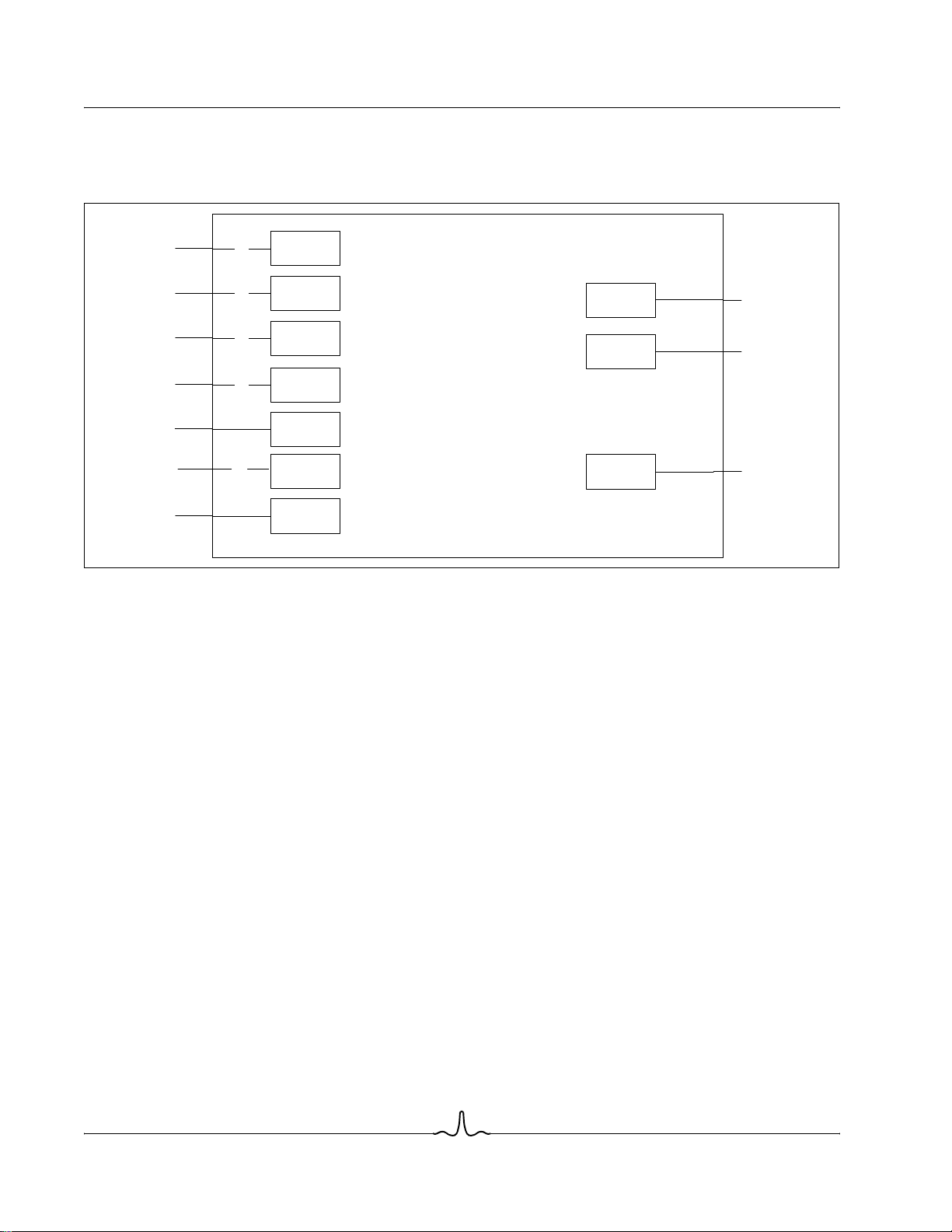
BCM7405 Preliminary Hardware Data Module
Functional Description 06/29/07
DATA TRANSPORT I/O CONNECTIONS
Figure 1-4 illustrates the primary data transport I/O connections to the chip pads.
Input
pads
Input
pads
Input
pads
Input
pads
Input
pads
Input
pads
Input
pads
IB0
IB1
IB2
IB3
IB4/IBP4
IB5
INPUT
BAND0
INPUT
BAND1
INPUT
BAND2
INPUT
BAND3
INPUT
BAND4
INPUT
BAND5
MCARD
IN
RMX/RMXP
RMX
MCARD
OUT
Output
pads
Output
pads
Output
pads
Figure 1-4: Data Transport I/O Connections Diagram
Data Transport Input Bands
The data transport module provides six serial transport stream inputs. The data transport can support up to six active
external input bands with a maximum input rate of 100 Mbps per input. These six input bands are available as inputs to the
PID parsers, the PCR modules. There are several formatting options available for each of the transport stream inputs to
handle the many formats that are known to exist. Each input is independently programmed for these options in case different
inputs use different formats. For example, bit-wide and byte-wide serial sync inputs are supported as well as active low sync
signal input. Each input can be programmed to latch incoming data on either edge of the input clock. For serial MPEG stream
inputs, there is also the capability to perform sync detection in case the sync signal is not available. For other available
options, refer "Data Transport" in the BCM7405 Programmer's Register Reference Guide. The data transport module
provides one external parallel transport stream input. Input band 4 can be used as either serial or as parallel format.
Throughput Data Rate
The data transport module supports a maximum combined transport stream burst rate that can be greater than 216 Mbps
based on usage. As packets rejected by the PID parsers are discarded, a DRAM rate smoothing buffer called the RS buffer
is used to convert this burst rate to average rate of up to 216 Mbps after PID filter. Thus, the data transport module supports
a combined transport stream average rate after PID filtering of 216 Mbps. The RS buffer basically consists of transport
buffers for audio/video/system and the video multiplexing buffers as per MPEG buffer model.
Use of Multi-Stream CableCard limits this combined transport stream average rate to 200 Mbps. The downstream
descrambler throughput can also affects the combined transport stream average rate. The downstream descrambler itself
has a throughput of 216 Mbps. However, for streams that need Multi2 descrambling, this throughput rate is derated to 157
Mbps.
Broadcom Corporation
Page 1-16 Data Transport Processor Document 7405-1HDM00-R
2/24/2008 9T6WP
Page 31

Preliminary Hardware Data Module BCM7405
06/29/07 Functional Description
PID Parser
The data transport module supports six independent front-end PID parsers and five playback PID parsers. A 255-entry PID
table is used to compare with the PIDs of the selected transport streams. Each PID channel consists of a primary PID filter
and an optional secondary PID filter. With all secondary PID filters enabled, this corresponds to a total of 255 simultaneous
PID filters.
When a primary PID filter does not have a secondary PID filter enabled, that primary PID filter operates without any
restriction. When the secondary PID filter is enabled in a PID channel, both the primary and the secondary PID filters in that
channel are restricted in the following ways:
• Both PIDs should be from same band (tuner input or playback channel).
• If conditional access descrambling is required, both the primary and the secondary PIDs must use the same key.
• The primary and secondary PIDs cannot use the message filters. The message filters can be configured to save the
PID filtered transport streams directly into message buffers.
• The primary and secondary PIDs in this channel cannot support Passage.
• The primary and secondary PIDs in this channel must have the same destination (i.e. record channel, message buffer,
video/audio decoders, Remux).
The data transport has a message DMA which includes 512 4-byte generic section filters and 128 DMA buffers which can
be used for PSI or PES filtering. PES and PSI filtering cannot share the same DMA channel. Data from PID channels 0-127,
after further processing, may be sent to one or more of the 128 message buffers. Data from PID channels 0-127 may be
used by the RAVE (record, audio and video interface engine) or output via the Remux module. Common values among all
parser bands are processed independently. Each PID parser examines the continuity counter and rejects duplicate packets
for the PIDs it is programmed to accept. Each parser also generates error interrupts for short packets and for continuity count
errors.
PID Duplication is not supported, i.e., same PID and BAND value can not be programmed in multiple PID channel locations.
Each of the 128 PID channels is programmed independently for the type of filtering (PSI, PES, or SAVE_PACKET_EN) to
be applied on that channel. The resulting filtered data from these PID channels are sent to the respective message buffers.
The following constraints must be followed when programming the PID channel filtering options provided by the data
transport processor:
• For any single PID channel, only one type of packet filtering option (i.e., PES, PSI, or SAVE_PACKET_EN) is allowed.
Packet Input Buffer
The packet input buffer stores all of the transport packets that are accepted by the PID parsers. The input buffer then outputs
these packets to the subsequent processing blocks in the order in which they were received. The maximum combined data
rate of packets through the input buffer is 216 Mbps after PID filtering. Packets not accepted by the PID filters are discarded
and not stored.
Packet Timestamp
The input buffer maintains a separate 32-bit timestamp counter for each PID parser which can be locked to any one of the
timebases or to a free running 27-MHz clock. Each packet that is accepted by a PID parser can be optionally stamped using
this local timestamp counter. This timestamp can be used for record, playback with pacing, or PCR correction for remux.
PCR correction is necessary while outputting from the Remux, as packets can remain in the multiplexing buffers for a
variable length of time.
Broadcom Corporation
Document 7405-1HDM00-R Data Transport Processor Page 1-17
2/24/2008 9T6WP
Page 32

BCM7405 Preliminary Hardware Data Module
Functional Description 06/29/07
Timestamp format is programmable—32 bit straight binary or modulo 300 for the nine LSB, similar to the MPEG PCR.
Timestamp format can be selected independent of the transport packet format. Playback pacing supports both timestamp
formats. However, PCR correction can only be done when the selected timestamp format is the same as the PCR format.
In other words, hardware cannot convert the local timestamps to the format of the PCR within the transport packets.
As the packet is being output from the data transport, the only place that the timestamp value can be output with the packet
is at the record. Here, record can select one of the two timestamp modes. In the normal mode, the 32-bit recorded timestamp
consists of a 4-bit parity and 28-bit timestamp value. In the special mode, the 32-bit recorded timestamp consists of a 2-bit
user-programmable value and a 30-bit timestamp. A preset starting timestamp value can also be synchronized with the first
recorded packet. In addition to recording timestamps with the data, record channel can also attach the timestamp with each
SCD entry generated.
During playback, the timestamps recorded with the data can be used to pace the playback data. These timestamps can also
be used to do PCR correction if playback data is to be routed out remux. Playback can also extract the two userprogrammable bits in the timestamp (for special timestamp mode), and present them in registers for the host CPU to read.
Playback pacing must have same programming of the format and mode of the timestamp as that during record.
Record function of time interval packet counting, and PCR out of range detection, will be performed by the host CPU
software. The purpose of the time interval packet counting is to later navigate within the recorded stream, performing jumps
in playback with respect to time. This function is best implemented using the record generated SCD, which provides very
accurate navigation data such as picture starts, etc. The SCD also stores PCRs found in the stream, together with their
corresponding local timestamp. This allows the software to more accurately determine the PCR errors, and to determine
unmarked PCR discontinuities. More robust algorithms can be performed by the host CPU to support this function.
PID/Packet Substitution and Generation Module
To provide facilities to adjust the SI PIDs after an MPEG or DIRECTV stream is filtered by the PID filter to remove PIDs, six
PID substitution and generation (PSUB) modules are included. The output from each of these PSUB modules are available
simultaneously to all output modules—record, A/V channels, remux, message filters. Each PID substitution and generation
module can receive input from one input band. All six modules can operate on the same or six different input bands.
Each module provides one DMA channel for packet generation. The inserted data is in linked list buffers in external DRAM,
exactly as record and playback. This packet generation process is fully automatic. The host CPU needs only to generate the
linked list and the packet buffers, program the linked list start pointer, and arm the insertion control. The module automatically
reads the linked list, then reads the external DRAM buffer content, and performs the insertion. The insertion buffer can be
any size and located anywhere in memory (32-bit address). Packets to be substituted are removed by the PID parser.
Each PSUB module is designated as either high priority or low priority, but not both. When more than one PSUB modules
are enabled and operate on the same input band, the high priority module will output all its packets before the low priority
module. If the low priority module is also programmed, and in the middle of output, the high priority module will immediately
start to output after the current packet, delaying the low priority module until all its packets are output. Then the low priority
module will resume its output. Among PSUB modules with same input band and same designated priority (all high or all low),
module 0 will have highest priority, then module 1, 2, 3, 4, and 5. Output from the PSUB modules is on a space available
basis (see below). Optionally the data transport can jam the input (asserting FORCE_SUB), which means packets are
immediately dropped to allow insertion. All six PSUB modules have an individual FORCE_SUB control. The overall priority
of insertion among PSUB modules that operate on same input band is as follows, from highest to lowest:
Broadcom Corporation
Page 1-18 Data Transport Processor Document 7405-1HDM00-R
2/24/2008 9T6WP
Page 33

Preliminary Hardware Data Module BCM7405
06/29/07 Functional Description
1 PSUB0 High priority
2 PSUB1 High priority
3 PSUB2 High priority
4 PSUB3 High priority
5 PSUB4 High priority
6 PSUB5 High priority
7 PSUB0 Low priority
8 PSUB1 Low priority
9 PSUB2 Low priority
10 PSUB3 Low priority
11 PSUB4 Low priority
12 PSUB5 Low priority
There is a hardware timer per module, allowing automatic repeat of the entire insertion for each module. This timer
determines the packet-to-packet interval. This interval will have range from 14 us up to 0.9 second. This timer also allows
time borrowing. This means that if the last insertion buffer took longer than the programmed interval, the current insertion
will start immediately, and the current interval is shortened by the same amount. The timer in fact ticks at a constant rate,
without restarting after each insertion.
Each DMA channel has a start, stop, pause, and resume control to allow interruptions by the host CPU.
Status and an optional interrupt will inform the host CPU that the insertion has occurred, and the host CPU can then load
new data into the insertion buffer, and re-enable the packet generation. At any time, the host CPU can read the link list DMA
control to find out the address of the current buffer read pointer for each channel. A repeat bit allows using the previous link
list. The DMA rate will sustain insertion of every packet being adjacent, except at link list read times.
The insertion modes and rates can be configured dynamically, when the module is already enabled, the new modes and
rates take effect at the beginning of every packet arrival.
Each group of inserted packets is given a PID channel number, which can be the same or different between insertions. This
PID channel number is used in the stream selection process of all output modules—record, A/V channels, remux, and
Message filters.
Multistream CableCard Interface
The interface is an implementation of the OpenCable Advanced Multistream POD Interface Specification (OC-SP-CCIF2.0D01-040831). When Multistream CableCard function is enabled, transport data from the input buffer can be routed out of
the data transport module for processing by an external AMS-CableCard module via MPOD interface.
Transport packets (both DIRECTV and MPEG) are put into a 200-byte packet format defined in the AMS-CableCard
specification. DIRECTV packets are packetized within dummy MPEG packets before being sent to the AMS-CableCard
module, and de-packetized after returning from AMS-CableCard module.
Packet band, null packet, and timestamp information transmitted in the AMS-CableCard header is recovered from the
header when the data is received back into data transport. The extracted DIRECTV and MPEG packets recovered from the
AMS-CableCard input stream are processed through a secondary PID parser to recalculate PID match and channel
information. The recovered steam is then routed into Conditional Access Descramblers.
Broadcom Corporation
Document 7405-1HDM00-R Data Transport Processor Page 1-19
2/24/2008 9T6WP
Page 34

BCM7405 Preliminary Hardware Data Module
Functional Description 06/29/07
Condition Access Descramblers (The Downstream Descramblers)
The data transport module provides a DVB, 1DES, 3DES, AES, and a Multi2 descrambler for Conditional Access for up to
128 PID channels which may include video, audio, and data streams.
The DVB engine supports full and conformance mode. It also supports both transport and PES level descrambling.
The 1DES, 3DES and multi2 supports ECB and CBC mode with selectable residue termination modes of partial block
unscrambled, residual block termination, and cipher-text stealing. CBC mode with cipher-text stealing is not a reversible
mode.
The Multi2 descrambler supports four separate 256-bit system keys, selectable for each PID channel. Thus, it supports up
to four different Multi2 system headends. The descrambler descrambles the packet payload as usual, using termination
modes of cipher text stealing, residual termination, or partial block unscrambled. The Multi2 max round count is 32. Valid
values are 0x20, 0x18, 0x10, and 0x08.
The AES descrambler supports only CBC mode. Keys and modes are configured in a 896x64 key table. Each PID channel
has index entry to point a set of keys and modes to be used for descrambling. Multiple PID channels can point to same or
different key sets.
The descrambler also extracts the 2-bit scrambling control from each transport packet for each PID channel, and save them
in registers for the host CPU to read. The host CPU can always read the latest scrambling control bits for each channel, and
a per PID status bit signals whether the scrambling bit is valid since the last read.
NDS ICAM Module
An NDS ICAM 2.2a module is supported.
Copy Protection
Memory to Memory DMA with Security
For copy protection, we support a memory to memory DMA subsystem that can scramble or descramble data. The Mem-toMem Security module performs the scrambling/descrambling function of that subsystem. The Mem-to-Mem DMA portion of
the subsystem resides outside data transport. This module also supports Transport packet parsing function, so only payload
data is scrambled/descrambled.
The Mem-to-Mem Security module may be programmed to perform the following functions:
• ECB mode scrambling/descrambling with 3DES core in ABA or ABC modes (64 bits data, 128/192 bits key).
• CBC mode scrambling/descrambling with 3DES core in ABA or ABC modes (64 bits data, 128/192 bits key).
• ECB mode scrambling/descrambling with DES core (64 bits data, 64 bits key).
• CBC mode scrambling/descrambling with DES core (64 bits data, 64 bits key).
• ECB mode scrambling/descrambling with AES core (128 bits data, 128/192 bits key).
• Counter mode scrambling/descrambling with AES core (128 bits data, 128 bits key).
• ECB mode scrambling/descrambling with C2 core (64 bits data, K bits key).
• C-CBC mode scrambling/descrambling with C2 core (N x 64 bits data, K bits key).
• Sector mode data descramble with CSS core (2048 x 8 bits data, K bit key).
• CBC mode scrambling/descrambling with AES core as defined by AACS and DTCP (128 bit data, 128 bit key).
• Supports 96 x 64 bit key table. Each key set requires one 64 bit mode word. Cores that use longer key length will use
multiple keys.
• M6 scrambler/descrambler for DTCP.
Broadcom Corporation
Page 1-20 Data Transport Processor Document 7405-1HDM00-R
2/24/2008 9T6WP
Page 35

Preliminary Hardware Data Module BCM7405
06/29/07 Functional Description
PES Parser
The PES parser delineates PES packets and sends them to the message buffers. Any number of the PID channels 0-127
can be enabled for PES processing. When a complete PES packet is received, a data available interrupt is generated by the
message buffer manager. The PES parser checks for PES packet lengths and generates length error interrupts. PES
Padding streams (i.e., PES messages with stream_id of 0xBE) are removed by default, or optionally retained. When stored
to memory, padding bytes (0x55) are optionally added at the end of each PES packet to word align to 32-bit boundaries in
the message buffers. During data transport playback, the padding bytes are removed.
The PES Parser checks for PES packet length and can generate length error interrupts if enabled. It uses the
payload_unit_start_indicator bit in the transport packet to detect the beginning of the PES packet. A length error is generated
whenever the end of a PES packet does not coincide with the end of a transport packet or the payload_unit start_indicator
is received prior to the end of the current PES packet. Only PID channels 0 to 127 can be routed to PES parser.
PSI Section Filter and Processor
The PSI processor delineates MPEG PSI section messages and performs section filtering, SAM filtering, and CRC checking.
It also performs similar processing for DIRECTV messages.
The PSI processor for this device supports sixteen banks of 32 4-byte generic filters for a total of 512 generic filters. Banks
of 4-byte generic filters can be cascaded to make up groups of filters that are effectively up to 64 bytes wide. Each of the
PID channels 0-127 can independently select one group of filter. Each PID channel can use any number up to 32 filters in
that group. Furthermore, each section filter can be applied to any number of these 128 PID channels. Each PID channel can
also independently select its own programmable generic filter offset.
For MPEG mode only, the SAM filters examine the PSI section header syntax, and the filters on address compare with the
special mode addresses. There is one 40 bit physical address and one multicast 24 address. There are two-40 bit network
addresses and two multicast 40 addresses. The network addresses and multicast 40 addresses each support a wildcard of
4 or 8 bits. In addition, each PID has four multicast 16 addresses. The SAM filter also compares the table ID with a set of
lower and upper table ID limits and rejects the sections that fall within these limits. Each of these addressing modes can be
enabled on a per PID basis for PID channels 0–127.
The PSI processor verifies section starts, removes padding bytes, and performs CRC checks. Messages which are greater
than 4096 in length can be optionally rejected and messages which are less than seven in length can be optionally rejected.
If a CRC check fails, the section is rejected. There is a per PID disable for the CRC check. There is also an option to modify
the message as it's being saved to DRAM buffer by one of the following methods:
• Replace the CRC with a sentinel.
• Replace the CRC with the section filter match tag.
• Append the message with the section filter match tag.
The option to modify the message is enabled on a per PID basis. The filter match tag options provide a way to identify which
filtering options were used to accept different PSI messages within a common PID stream. When using the filter match tag
options, only one PID channel is opened. All PSI messages for that PID will be saved to a single message buffer; and
software will use the filter match tag to identify which filtering options were used to accept different PSI messages for that
PID.
Each generic filter is comprised of 4 bytes of coefficients, 4 bytes of inclusion masks and 4 bytes of exclusion masks. The
inclusion and exclusion masks work independently during the filter compare process. For a particular section filter to accept
a message, all of the message bits marked for inclusion (i.e., MASK = 0) must match the corresponding coefficient bits, and
at least one of the message bits marked for exclusion (i.e., EXCL = 0) must mismatch the corresponding coefficient bits.
Disabled message bits (i.e., MASK = 1 and EXCL = 1) are not considered.
Broadcom Corporation
Document 7405-1HDM00-R Data Transport Processor Page 1-21
2/24/2008 9T6WP
Page 36

BCM7405 Preliminary Hardware Data Module
Functional Description 06/29/07
Each enabled generic filter is applied to MPEG section bytes 0-3, excluding byte 2. Banks of 4-byte generic filters can be
cascaded to make up groups of filters that are effectively up to 64 bytes wide.
The PSI processor also supports dynamic reconfiguration of a filter for an active PSI channel. This includes dynamically
adding, removing, or reprogramming of an existing filter.
Memory Buffer Manager
The data transport module provides for 128 independent message buffers (in external system memory) corresponding to
PID channels 0–127. Each message buffer stores data that comes from the respective PID channel. The type of data stored
to the message buffer (PSI section, PES packet, or transport packet) is determined by the filtering selections made for each
PID channel.
The message buffer manager collects all accepted data and sends it to one of more of the 128 corresponding message
buffers. Each message buffer can start on any 1 KB address boundary, and can be from 1 KB to 512 KBs long. The message
buffer manager maintains a pointer to the last valid memory location of each buffer (such as the valid_pointer), while the last
read memory location is supplied by the microprocessor (the read_pointer). If unread data is present, an interrupt may be
generated. The message buffer manager waits until the entire delineated message (PES packet, PSI section, or transport
packet) is verified and written to memory before it updates the buffer valid pointer. Each message is optionally 32-bit word
aligned. When word-align is enabled, a partial word at the end of a message (or transport packet when using
SAVE_PACKET_EN mode) is filled with bytes of 0x55.
Interrupt Controller
The interrupt controller generates interrupts for any of the data available, status or error conditions. Each of these conditions
are individually maskable. The interrupt status registers can be read to determine the conditions, and written low to clear the
interrupts. Some of the status and error conditions are indicated on a per PID basis. The various interrupt conditions that
may occur in the data transport module are divided into groups:
• Status Interrupts
• Message Buffer Overflow Interrupts
• Message Buffer Data Ready Interrupts
Each group of interrupts contains up to 64 unique interrupt conditions. Each of these groups generates a unique interrupt
signal which is output from the data transport module to the higher level interrupt controller.
Record Audio Video Engine (RAVE)
The data transport module has a programmable audio/video transport demultiplexer called RAVE. In addition to the audio/
video parser functions, RAVE supports record functionality for PVR applications. It accepts an MPEG or DIRECTV Transport
stream input from one or more input bands, and Transport, PES or ES streams from one or more playback bands. RAVE's
output format can be ES, PES, or Transport data for PVR. RAVE supports 24 channels. Each RAVE channel can be
configured as a record channel for PVR or as an AV channel. Each record channel can be configured for one to eight SCD
or one TPIT (maximum of five in the system). The AV channels are used for interface to the audio/video decoders via the
external memory subsystem.
Record
Each record channel can be used to record transport streams for up to 128 PID channels. The Record channel is allocated
two external DRAM buffers; one for data, and the other for index table entries. Each channel's index table descriptor buffer
contains entries which points to relevant locations within the data buffer, such as start code locations, PTS information, etc.
Each record channel can support up to four types of entries. These include a Start Code Detect entries, Transport Parser
Index Table (TPIT) entries, seamless pause entries and/or a PTS entries that can be used to build start code tables or
Broadcom Corporation
Page 1-22 Data Transport Processor Document 7405-1HDM00-R
2/24/2008 9T6WP
Page 37

Preliminary Hardware Data Module BCM7405
06/29/07 Functional Description
transport field tables which can then be used during playback to perform trick modes. RASP, as defined by NDS, can be
supported using TPIT. Up to five record channels can be configured for the TPIT function.
A local timestamp is generated at the input buffer via an internal counter using a 27-MHz clock selectable from any of the
three available locked timebases, or the free-running system clock. The local timestamp can be prepended as a 32-bit field
to each recorded transport packet. The format of the 32-bit timestamp filed is programmable. In one mode, this field contains
a 28-bit local timestamp plus a 4-bit parity which can be used during playback to transmit the packets at a rate equivalent to
when they were recorded and can be used for PCR correction in the Remux modules. In another mode, the upper two bits
of the 32-bit timestamp field are user programmable with the remaining bits being the timestamp.
Record Channel’s Index Table Generation
Index table generation is a function that is supported in the record channel. Although this function handles more than just
start code table entries, it will be referred to as the SCD (start code detector) in this document.
The SCD records the positions of PES packet header stream_id's and elementary stream start codes within a recorded
transport stream for a given PID. There are two transport modes of operation: MPEG and DIRECTV. The data structure for
data stored in the memory buffer is a start code index table that is detailed in the Record Index Table Definition section.
Within each transport mode (MPEG and DIRECTV), there are four index table modes supported. All modes utilize a 6-word
index entry. Four index entry types are supported: Start Code (SC), Presentation Time Stamp (PTS), Transport Field (TF),
and Seamless Pause (SP). The following describes the four entry types:
1 The SC index entry provides offsets to start-code locations within the associated record buffer.
2 The PTS index entry provides PTS values extracted from the recorded stream.
3 The TPIT transport field parser stores transport field index entries. For the on-change conditions, an initial entry is made
for detection of the first PID. For example, if the first packet for a PID with the transport_scrambling_control_change_en
bit set has a scrambling control of 10, an index table entry is stored for the transport_scrambling_control_change
condition with the transport_scrambling_control_change bit set and the actual value of the scrambling_control of 10 is
stored in the scram_control field.
4 The seamless pause feature is intended for use with playback. It allows live viewing of a program with the capability of
pausing the program. The program is initially viewed without going through the record/playback path. This eliminates
channel change latency incurred when going through this path. When the user wishes to pause the program, a record
channel must be enabled with the appropriate PID channels selected for record. Then REC_PAUSE_EN is asserted.
This assertion prevents the selected PID channel data from being sent to the audio/video decoders. The user sees this
as a pause. Once REC_PAUSE_EN is set, the next packet that is recorded has a seamless pause entry made in the
record index table (if the index table is enabled). When the user wishes to resume the program, the stream now comes
from a playback channel instead of the live channel. The index table entry made for seamless pause is used to determine
where to start the playback.
SCD Elementary Stream Start Code Detection
The SCD module parses the system transport and PES layer to find elementary stream (ES) start codes. First, the transport
layer is parsed to determine what is transport payload. In PES mode, the PES layer is parsed to find the desired ES (all data
besides the PES header).
The data that is determined to be the desired ES is fed to a start code detector that looks for the pattern 000001XX where
XX is a start code.
Transport packet synchronization and filtering is done using a packet sync signal, a host CPU programmed PID and
transport mode specific criteria. The payload data is found in the following manner:
Broadcom Corporation
Document 7405-1HDM00-R Data Transport Processor Page 1-23
2/24/2008 9T6WP
Page 38

BCM7405 Preliminary Hardware Data Module
Functional Description 06/29/07
1 The packet sync signal is used to determine the start of a transport packet, regardless of the current state of the transport
parser.
2 The PID must match the host CPU programmed packet ID.
3 In MPEG mode, the adaptation control bits are checked. The adaptation field the packet is not considered as PES
payload.
4 In MPEG mode, the payload unit start bit is fed to the PES layer parser. However, it is not used at the transport layer.
In PES mode, data that is determined to be transport payload is fed to PES layer parser. As noted above, the payload unit
start bit is also given to the PES layer parser in MPEG mode. The PES layer parser must support ES start code detection
across PES packets. In order to do this, ONLY the PES_packet_data_byte bytes are fed to the ES start code detector. The
ES data is found in the following manner:
1 Once any PES packet start is found, an entry is made for it in the Start Code Index Table.
2 If present in the PES header, the PTS value will be extracted if the SCD_PTS_MODE bit is set in the SCD control
register. This value will be stored in the Start Code Index Table if its corresponding PES packet start is stored in the index
table.
3 In MPEG mode, an asserted payload unit start signal indicates the next PES payload byte is the first byte in a PES
packet, regardless of the current state of the PES layer parser. This is the only method used in MPEG mode to determine
PES packet starts. The stream_id must match the programmed range of stream_id's.
Record SCD ES Start Code Storage
Once a start code is found within the elementary stream, several conditions must be met before the start code will be stored
in the index table. The method of storing ES start codes is intended to provide pointers to the locations of video access units,
picture start codes, and the start of the first row for each access unit. The following lists the conditions for storing start codes:
1 Start codes are stored in an alternating manner between two types: First slice start code 01 and Non-slice start codes
(00, B0-FF). Once a start code 01 is stored, it will not be stored again until a Non-slice start code is stored. Once any
non-slice start code is stored, only picture start codes will be stored until the next first slice start code is stored.
2 In addition to the above storage sequence, any start-code values within the range specified by the SCD range registers
are stored.
3 All picture start codes are stored (SCV = 00).
4 PES header start codes are not considered in this sequence. Only the start codes within the ES are used to determine
which ES start codes to store.
5 In addition to the start code value, all index entries contain the next two bytes following the start code value.
6 If a continuity count error or TEI error is detected, an exception is made to the above sequence. In addition to the normal
sequence, any slice start code (SCV 01-AF) will also be stored to report the error. After the error is reported the normal
sequence resumes.
Transport Parser Index Table (TPIT)
The TPIT extracts fields from MPEG transport packets and creates index table entries if the fields match programmable
criteria. External packet attributes can also add entries to the record index table. External packet attributes come from other
modules. When external packet attributes are detected, further filtering by enables/PID matching is performed to determine
if a record index table entry should be created.
• If a PID match is found by the record PID parser module, fields in the transport packet are compared against the
corresponding filter. Depending on the filter results, an index table entry can be made.
• Also, if a PID match is found, certain state bits are stored. For example, if a PCR exists in the packet, the PCR value is
stored. After the filter compare, the scrambling control bits are stored to assist with detection of scrambling control
changes.
Broadcom Corporation
Page 1-24 Data Transport Processor Document 7405-1HDM00-R
2/24/2008 9T6WP
Page 39

Preliminary Hardware Data Module BCM7405
06/29/07 Functional Description
There are three counters in the transport field parser:
• The packet counter: The packet counter counts all packets that are recorded. The packet count at the time an index
table entry is made is part of the entry.
• The record timer: The record timer keeps a running count of time since the record session started. The value of the
record timer at the time an index table entry is made is part of the entry.
• The idle timer: The idle timer counts the time between recorded packets. If the time exceeds a programmable timeout
value, an event is entered in the index table, if enabled. The idle timer repeats the timeout until a packet is received.
Audio/Video Interface
RAVE interfaces with the audio/video decoders via external DRAM buffers. Each AV channel is allocated two external DRAM
buffers; one for data, and the other for descriptors. Each channel's descriptor buffer contains entries which points to relevant
locations within the data buffer, such as start code locations, PTS information, etc.
These descriptors are used by the video and audio decoders to perform frame synchronization, error recovery, timestamp
management, and various other functions.
Each AV channel is fully independent of the other ones, and can be mapped to a separate audio or video decoder. The AV
channels can accept data in any of the following input formats:
1 MPEG transport (from live or playback source)
2 DIRECTV transport (from live or playback source)
3 PES (playback source)
4 ES (playback source)
5 Program Stream (playback source)
The AV channels also support the following output formats to the downstream decoders:
1 Transport output (from transport input)
2 PES output (from transport or PES input)
3 ES output
AV channels support removal of emulation prevention bytes for AVC and VC-1 formats. They can also assist the downstream
decoders in performing frame synchronization.
Playback
The data transport module supports five independent playback modules. The following description is for a single playback
module.
The playback function is used to provide either MPEG Transport Stream (TS), DIRECTV transport stream, PES, ES, or
Program Stream data to the audio decoder and video decoder and/or to the Remux modules. Additionally, the playback
function can route data from memory though the data transport block for PID parsing, descrambling and/or filtering to be
recorded, stored in the message buffers, or routed to RAVE and/or high-speed interface. The playback module supports
transport stream with or without local timestamps. The host CPU is responsible for putting the data into external DRAM from
wherever the data is really being sourced (i.e., hard drive, internet, transport memory buffer, etc.) Once the data has been
put into external DRAM, the playback module can be enabled to read the data from external DRAM and deliver it to RAVE
and/or to the high speed transport and Remux modules. The playback circuit also uses linked-list descriptors for buffer
management.
Broadcom Corporation
Document 7405-1HDM00-R Data Transport Processor Page 1-25
2/24/2008 9T6WP
Page 40

BCM7405 Preliminary Hardware Data Module
Functional Description 06/29/07
The playback module also includes a pacing function which can optionally pace the playback data using the local data
transport timestamps (when the playback data was recorded with timestamps).
Playback Sync Extractor
The playback sync extractor engine generates the sync signal for TS and PES streams which are played from a playback
memory buffer by the playback module. This sync signal is then used by the receiving modules (high-speed transport,
Remux, transport record and the audio/video output buffer) to delineate the transport or PES packets. There are five modes
of operation:
• TS1, which is used for MPEG transport stream playback. The length of transport packets is programmable. The sync
detect engine locks to the transport packet sync byte 0 x 47. When the engine is not locked to the playback stream,
data is not output and it flushes the data until lock is achieved.
• TS2, which is used for DIRECTV transport stream playback.
• TS Blind. The TS1_BLIND and TS2_BLIND modes are optionally used for MPEG and DIRECTV, respectively, to
playback any transport stream having a constant packet length. The packet length is programmable. Because this
mode counts bytes and outputs a sync signal, it requires the packets to be stored precisely into the playback memory
space with the first byte of playback being the start of a packet. All data is output, none is flushed or skipped due to not
being in sync as in the TS1, TS2, and PES modes of operation.
• PES, which is for PES packet stream playback with support for lengthless PES. The sync detect engine locks to the
PES start code (0x000001) and the stream ID which is a programmable valid range nominally set to 0xBC to 0xFF.
When the engine is not locked to the playback stream, data is not output and it flushes the data until lock is achieved.
The PES packets with a stream ID outside of the programmed valid range are dropped, and the out-of-sync condition is
indicated.
• Bypass, where the sync detect only passes the incoming data/valid along with the incoming new program playback
signal to the data/valid/sync outputs, respectively. The new program signal is sent out as the sync bit. All data is output,
none is flushed or skipped due to not being in sync as in the TS1, TS2, and PES modes of operation.
The sync extractor also generates an out-of-sync real-time status indicator and an out-of-sync interrupt which occurs when
the engine transitions from in-sync to out-of-sync. The sync extractor drops data when in the out-of-sync state.
Remux Module
The Remux module combines two transport streams and outputs the resultant serial stream using three pins (clock, data,
and sync). The Remux module consists of an input multiplexor, a PID remapper, a packet buffer, a PCR correction unit, a
packet substitution unit, and an output formatter. The input multiplexor mixes any two streams selected from the pool of five
input bands, five parser bands (encrypted or decrypted) or a subset of the combined parsed-decrypted stream or parsedencrypted (such as, not decrypted) or the four playback streams and outputs the one resultant stream. The PID remapper
parses the selected input streams for up to 32 PIDs as defined in the Remux PID table and the PID can be modified to avoid
duplication in the combined stream.
Each remux input channel has both the Normal and All-pass modes of operation. In the Normal mode, only PIDs defined in
the Remux PID table are output, other PIDs are dropped. In the All-pass mode, all PIDs are output, and any PIDs in the
Remux PID table are remapped accordingly. The packet buffer is simply a FIFO ram to hold the packets and local
timestamps until it is time to output them. The packet buffer is maintained in system DRAM to give flexibility on the size of
the buffer. There is also a PCR correction, packet substitution and null packet generation module. A state machine driven
by an output request coordinates the output of packet data, with packet substitution, or generate null packets when
necessary. The Packet Substitution module allows certain transport packets to have their payload replaced with data that is
stored in the local Packet Substitution Table. Packets eligible for substitution are those with a particular PID and HD field.
The Remux packet substitution module allows up to two different packets to be substituted. Alternately, this module can
generate packets and insert them directly into the output stream. This module also substitutes a time-corrected PCR for
every packet containing a PCR. The PCR correction module calculates the difference between the packet timestamp and a
Broadcom Corporation
Page 1-26 Data Transport Processor Document 7405-1HDM00-R
2/24/2008 9T6WP
Page 41

Preliminary Hardware Data Module BCM7405
06/29/07 Functional Description
local timestamp clock, plus a programmable offset, and adds the result to the existing PCR when the packet is output. This
maintains the accuracy of the PCR in the time shifted output packet stream.
The sync output tags the beginning of each transport packet.
Note: When outputting a playback channel, the output sync signal is generated by the playback sync extractor
module, so the ability to tag every packet depends on the integrity of the playback data stream and the ability
of the sync extractor module to lock to the playback data stream.
Synchronizers allow the serial output of clock, data, and sync to be run from the following selected clocks:
• IB0-5
• 81 MHz
• 54 MHz
• 40.5 MHz
• 27 MHz
• 20.25 MHz
The data transport supports two equivalent Remux modules i.e., Remux0 and Remux1, each programmed independently.
Remux1 module can output data either in serial of parallel output format. In parallel output format data is 8-bit wide. Whereas,
Remux0 can output data only in serial format.
PCR Recovery Block
The data transport design supports two equivalent PCR recovery circuits, each programmed independently.
Each data transport PCR module is capable of extracting the PCR information from a selected packet stream and generating
Timebase pulses (Timebase is a 27-MHz pulse train in 108-MHz clock domain) output that can be used by rate managers.
Each PCR module is also used to send the extracted PCRs directly to the audio and video decoders to ensure that both
decoders are using the same PCR.
Each VCXO generating 27-MHz system clock is locked to corresponding timebase pulse output from pcr_tb_loop.
The PCR module is programmed by the host CPU to search for a given PID. For MPEG streams, each time a PCR is found,
the 33-bit base and 9-bit extension are captured into a register, and the phase compare interrupt is asserted. At the same
time, the PCR load interrupt is pulsed if the host CPU has rewritten the PID register (with the valid bit set), or discontinuity
has occurred since the previous PCR was found.
When the PCR load interrupt occurs, the captured PCR is loaded into the system time clock (STC) counter. For MPEG mode,
the STC is configured with a 33-bit base and a 9-bit extension so that the base counter increments once every 300 27-MHz
ticks of the extension counter. The STC base counter is available for reading by the host CPU.
When the phase compare interrupt occurs, the current STC base and extension are latched. The latched STC values are
then compared to the latest PCR base and extension. Loop gain constants (FILT_A, FILT_B and FILT_C) are programmable
by the microprocessor to provide a degree of control to this filter. Loop filter is first order IIR filter. All LPF arithmetic is
saturating and phase saturation interrupt is generated if final output saturates.
Timebase loop allows the load integrator value to rapidly change the output frequency, but Broadcom does not normally
recommend this.
Two soft resets are also provided—one for the entire PCR module, and one that only resets this packet processor portion.
Broadcom Corporation
Document 7405-1HDM00-R Data Transport Processor Page 1-27
2/24/2008 9T6WP
Page 42

BCM7405 Preliminary Hardware Data Module
Functional Description 06/29/07
The PCR module also is used to aid in the detection of unmarked PCR discontinuities. The module monitors the PCR base
error (which already exists in the PCR tb_loop module). The module checks the resulting base error for each received PCR
against the programmable threshold, which is a 32-bit value with a default of 255 and has units of 27/300 MHz for MPEG
mode. If the threshold is exceeded one time, the one_pcr_error_interrupt is asserted. If the threshold is exceeded twice in a
row, the two_pcr_error_interrupt is asserted. The two_pcr_error_interrupt is provided so that single PCR errors can be
ignored. Both interrupts are maskable. Since the base error can be both positive and negative, the approximate absolute
value of the base error is compared to the threshold.
In addition to extracted PCRs from the transport stream, the PCR block can lock Timebase outputs to one of following
timebase references (asynchronous to internal system clock).
2
• I
S 0
• 656 Hsync0
• 656 Vsync0
• 656 Fsync0
The time-base reference is muxed at input level of LOOP control, it avoids generation of abrupt frequency change affected
by VCXO control changes during channel change (e.g., digital to analog).
Serial STC Broadcast Module
Data transport supports a global STC counter and a broadcast STC serially to Audio/Video decoders. Also, STC Broadcast
block generates PCR_OFFSET for arrival of each PCR, which is used by audio/video decoders for PTS time management.
BROADCOM SECURITY PROCESSOR
The Broadcom Security Processor (BSP) enables Set-Top Box (STB) chips with strong security for high performance
multimedia applications that deal with high-quality video and audio. These applications can range from single-purpose
conditional-access (CA) for watching-TV-only STB to multi-purpose copy-protection (CP) for Personal Video Recorder
(PVR) STB and digital right management (DRM) for multimedia gateway system. Broadcom Security system implements
various security components required in satellite and cable STBs and various CA and CP standards, such as CP for
CableCard and Secure Video Processor (SVP), but its orientation around a powerful Broadcom Security Processor (BSP)
makes it capable of implementing a variety of security algorithms, whether open or proprietary. More than just an integration
of STB security components together, Broadcom Security System design is an integrated security system controlled by BSP
with a small real-time OS kernel that runs on its own master processor. The Broadcom Security Processor (BSP) supports
various security features in an integrated STB SoC system such as:
• BSP includes One-Time Programmable Non-Volatile Memory (OTP NVM) security module. This module allows unique
keys and various security features and restrictions to be permanently programmed into a chip.
• BSP can provide key generation and management to the conditional access descramblers, e.g., DVB, DES
descramblers for removing conditional access encryption from incoming transport streams.
• BSP can provide key generation and management to the mem-to-mem scramblers/descramblers, for PVR copy
protection and other applications.
• BSP can provide protection to keys required by the interface security modules, e.g., High-bandwidth Digital content
Protection (HDCP) engine for high-bandwidth secure interface to digital displays.
• BSP can provide access control of various interfaces, e.g., remux interface.
• BSP can provide a secure environment and hardware acceleration for scrambling and descrambling the external data
with algorithm such as DES/3DES, AES, RS, and DH algorithms, etc.
• BSP can provide a secure environment for generating and verifying digital signatures, e.g., using RSA and DSA.
Broadcom Corporation
Page 1-28 Broadcom Security Processor Document 7405-1HDM00-R
2/24/2008 9T6WP
Page 43

Preliminary Hardware Data Module BCM7405
06/29/07 Functional Description
• BSP can perform external memory data validation. For example, BSP can verify the signature of the codes stored in, for
example, the off-chip program memory before the host CPU is authorized to execute these codes.
• Authentication process: Use of challenge-response mechanisms to activate various busses or test ports (PCI, EBI, and
JTAG)
ADVANCED VIDEO DECODER
OVERVIEW
The Advanced Video Decoder (AVD) module is a high-definition AVC/MPEG-2/VC-1/DivX/MPEG-4 P2 video decoder core.
The AVD module retrieves elementary stream video data placed into SDRAM by the data transport module, decodes the
video, and writes the decoded pictures back to SDRAM to be retrieved by video feeder in the video display subsystem.
The AVD core is capable of decoding one or more encoded elementary streams. The processing of such a stream has two
major components: front-end processing (the conversion of the code stream into fundamental components—motion vectors,
transform coefficients and the like) and back-end processing (actual generation and manipulation of pixels).
FGT block average logic is optional, it is available to compute block averages as an assist to the downstream FGT logic.
When enabled, this block monitors decoder pixel output and uses this data to calculate 8x8 block averages, which are written
to main SDRAM memory.
SUPPORTED PROTOCOLS, PROFILES, AND LEVELS
The AVD module can decode the following code streams:
• H.264/AVC main and high profile to level 4.1
• VC-1 advanced profile @level 3
• VC-1 simple and main profile
• MPEG-2
• MPEG still-picture decode
• MPEG-4 Part 2
• DivX 3.11, 4.11, 5.X, 6.X
The advanced video decoder module supports tools added in the AVC Fidelity Range Extensions (FRExt) amendment,
specifically 8x8 transform and Spatial Prediction modes, and adaptive quantization matrix required for High Profile support.
Additional capabilities include the following:
• Error concealment
• Multiple-stream support for up to sixteen low-resolution streams
Broadcom Corporation
Document 7405-1HDM00-R Advanced Video Decoder Page 1-29
2/24/2008 9T6WP
Page 44

BCM7405 Preliminary Hardware Data Module
Functional Description 06/29/07
AVC/H.264
• High profile, all levels up to and including 4.1
• Up to 40 Mb/sec. code stream bit rate
• Adaptive block size, quantization matrixes
The Advanced Video Decoder module decodes any bitstream coded with any combination of tools allowed under the Main
Profile as defined in the ISO standard 14496-10, (MPEG-4 Part 10). This includes any streams encoded by a baseline
encoder with the appropriate compatibility flag set for Main Profile operation.
The AVD module decodes bitstreams conforming to the restrictions set by Level 4.1 as specified in Annex A of ISO/IEC
Recommendation 14496-10 with the following restriction:
• Maximum encoded bit rate is 40 megabits per second.
This level supports pictures in the 1920x1088 interlaced format used by HDTV systems at a rate of 60 fields per-second.
VC-1
The AVD module supports VC-1 elementary streams in the following profiles and levels:
• Advanced profile levels AP@L0, AP@L1, AP@L2, AP@L3
• Main profile levels MP@LL, MP@ML, MP@HL
• Simple profile levels SP@LL, SP@ML
VC-1 decoding has the following restriction:
• Maximum encoded bit rate is 45 megabits per-second.
MPEG-2
• Main profile @ high level, main level
The AVD module supports MPEG-2 elementary streams encoded under the main profile at high level, as defined in ISO/IEC
Recommendation 13818-2, with the following restrictions:
• Maximum encoded bit rate: 125 megabits per-second.
• Internal data format: 4:2:0 format only.
MPEG-4 Part2
• MP4 SP up to HD with the exception of:
- reversible VLC codes
- data partitioning
• MP4 ASP up to HD with the exception of:
- global motion compensation
- 1/4-pel motion compensation
DivX
• Version 3.11, 4.11, 5.X, 6.X
- Progressive and Interlaced
- Up to HD support
Broadcom Corporation
Page 1-30 Advanced Video Decoder Document 7405-1HDM00-R
2/24/2008 9T6WP
Page 45

Preliminary Hardware Data Module BCM7405
06/29/07 Functional Description
XVID
XVID support with the exception of:
• global motion compensation
• 1/4-pel motion compensation
MPEG-1/H.261/H.263
FEATURES
• Error concealment
• SDRAM memory interface for code in and video out
• Five SDRAM clients, three linear, two pixel
• Single-clock design
• Multi-stream support, simultaneous HD + SD support for all protocols
SUPPORTED PICTURE SIZES
• MPEG-2: from 64x16 to 1920x1088
• H.264: from 64x16 to 1920x1088
• VC1: from 64x16 to 1920x1088
• MPEG4/DivX: from 64x16 to 1920x1088
• H.261/H.263: from 64x16 to 1920x1088
• MPEG-1: from 64x16 to 1920x1088
OUTPUT DATA FORMAT
The decoder stores images in a striped format that’s designed to optimize two-dimensional transfers. The images are stored
in 4:2:0 format, with luminance separate from chrominance. Picture buffer management is all under software control. The
decoder’s outer-loop RISC processor passes information about each display frame to an external video feeder, which can
pick it up out of memory.
The optional FGT block average logic writes averages for 8x8 block averages for a frame, and for the 4x8 sums for field 0
in interlaced mode. Each 8x8 average is 8 bits, and is stored in Y0-Y1-Y2-Y3-Cb-Cr order, in MB raster order. The averages
are written starting at the software programmed base address, and are written linearly without any holes.
The 4x8 sums are 16 bits each, and are also written out in Y0-Y1-Y2-Y3-Cb-Cr order. It uses two times as much space as
the averages.
Broadcom Corporation
Document 7405-1HDM00-R Advanced Video Decoder Page 1-31
2/24/2008 9T6WP
Page 46

BCM7405 Preliminary Hardware Data Module
Functional Description 06/29/07
AVD BLOCK DIAGRAM AND DATA FLOW DESCRIPTION
Figure 1-5 shows a block diagram of the Advanced Video Decoder module.
GISB
Outer
Loop
RISC
Entropy
Decoder
To/From DDR
via SCB
GISB Bridge
Inner
Loop
RISC
Symbol Interpreter
Spatial Prediction
Reconstruction
Motion Compensation
Deblocker
Video Frames
Reference Picture Data
via PFRI
Picture Buffers in DDR SDRAM
via SCB
Figure 1-5: Advanced Video Decoding Module Block Diagram
Coded data is presented to the AVD module as a linked list of packet entries, each entry corresponding to a network
abstraction layer (NAL) unit. Multiple streams are handled by multiple instances of linked lists. As NAL units accumulate in
memory, the outer-loop RISC processor examines them and passes them to an entropy decoder that reads the header
information. If the stream is CABAC-encoded, the outer-loop RISC then sets up the CABAC-to-BIN decoder to generate a
BIN representation. For CAVLC-encoded streams this operation is not necessary.
Once the outer-loop RISC determines that it has enough data to start decoding, it passes a structure to the inner-loop RISC,
which then starts inner-loop processing using one pass per image slice. The inner-loop RISC directs the symbol interpreter
to parse the data stream, from the BIN buffer for CABAC streams, or the code buffer for CAVLC streams. The symbol
interpreter converts the variable-length symbols to data values, and contains blocks to convert those values to spatial
prediction modes, motion vector deltas, and transform coefficients. These elements are then used by the back-end section
that performs the actual pixel reconstruction.
Broadcom Corporation
Page 1-32 Advanced Video Decoder Document 7405-1HDM00-R
2/24/2008 9T6WP
Page 47

Preliminary Hardware Data Module BCM7405
06/29/07 Functional Description
ADVANCED AUDIO MODULE
The audio module consists of two main modules: DSP subsystem and Audio I/O (AIO). The main modules of the DSP
subsystem consist of the DSP, data and instruction memories. The main functions of DSP subsystem include parsing audio
and timing data from data transport, decompressing compressed data, time stamp management, and processing PCM data.
The AIO consists of the FMM, one HIFIDAC, and audio input/output interfaces. The main functions include capturing I
data, mixing, and volume control of the playback data. It outputs data to I
2
S, SPDIF, HDMI formatter, RF modulator, and
HIFIDAC. Figure 1-6 shows the overall block diagram for the audio block.
2
S
To/From
Memory
Arbiter
and
Memory
Controller
Buffer
Block
DSP System
SRC
Capture 0I2S0 In
Data
Path
Micro-
Sequencer
PLL0
M * FS Audio Clock
PLL1
M * FS Audio Clock
M = 128, 192, 256, 384, or 512
Figure 1-6: Audio Block Diagram
IOP
Audio
DAC
I2S
Converter
SPDIF
Generator
Volume
Control
Analog
Out
To RF
Modulator
I2S0
Out
To
HDMI
Digital
Audio
Broadcom Corporation
Document 7405-1HDM00-R Advanced Audio Module Page 1-33
2/24/2008 9T6WP
Page 48

BCM7405 Preliminary Hardware Data Module
Functional Description 06/29/07
FEATURES
• The DSP System decodes any of:
- AAC-LC (ISO/IEC 13818-7) Input can be up to 5.1 channels with one coupling channel (dependent or independent)
and up to 288-kbps per-channel. Output is downmixed to two channels. Supported sampling rates are 16 kHz, 32
kHz, 44.1 kHz, and 48 kHz. Both ADTS and ADIF formats are supported.
- AAC-LC+SBR (ISO/IEC 13818-7, 14496-3:2001/AMD1, aka HE-AAC, aacPlus, AAC-SBR, AAC-he). High efficiency
AAC level 4 (5.1 channels), and low power SBR tool. Up to 288-kbps per channel. Supported sampling rates are 16
kHz, 32 kHz, 44.1 kHz, and 48 kHz.
- Dolby Digital Plus
- Dolby Digital (ATSC-A52/a). Input can be up to 5.1 channels. Output is downmixed to two channels. All sample rates
and all bitrates are supported.
- MPEG-1 (ISO/IEC-11172-3) Layer 1, 2, 3 (MP3). Input is 2.0 channels. All sample rates and bitrates are supported
except for the free bitrate.
- WMA, WMA Pro
• Supports:
- One stream of compressed data on SPDIF simultaneously with one stream of decompressed data on the dual
stereo DAC outputs.
2
- Compressed AAC, MPEG Layer 1, 2, and 3, DTS, and Dolby Digital on I
- Dynamic Range Compression on all algorithms
- Annex B and C for Dolby Digital 5.1 (ATSC A/52a)
- 16 kHz, 32 kHz, 44.1 kHz, and 48 kHz sample rates for AAC and MPEG
- 32 kHz, 44.1 kHz, and 48 kHz sample rates for Dolby Digital
- Two-channel down mix for streams with more than two channels
• Includes:
- One pair of Audio DACs for L/R channel outputs
2
-One I
S input and one I2S output for PCM at sample rates up to 96 kHz
- 3-D SRS Audio
• SPDIF output:
- Up to 24-bit PCM
- Sample rates of 16 kHz, 32 kHz, 44.1 kHz, 48 kHz, and 96 kHz
- Pass-through of Dolby Digital, MPEG, and DTS audio from DVD program streams
- Pass-through of Dolby Digital, MPEG, and AAC audio from transport streams
- IEC 60958 specification for linear serial data transmission
- IEC 61937 specification for non-linear serial data transmission
- PLL for low jitter output
• PCM mode processing: mute, mono left, mono right, mono, stereo
• Test tone generation
• Digital volume controls, digital mixing, and mute
• Robust handling of transmission errors
- Detection of output FIFO empty
- Detection of corrupted sync word
- CRC error checking
- Illegal stream checking (bit rate, sample rate, frame size)
S output
Broadcom Corporation
Page 1-34 Advanced Audio Module Document 7405-1HDM00-R
2/24/2008 9T6WP
Page 49

Preliminary Hardware Data Module BCM7405
06/29/07 Functional Description
OVERVIEW OF AUDIO MODULE
The BCM7405 audio core consists of DSP subsystem (RPTD) and audio input/output module (AIO). The RPTD is a DSP
system block for decompression of MPEG, Dolby Digital, MPEG-2 AAC, MPEG-4 AAC, and Dolby Digital Plus audio
services. The DSP system also supports a second digital audio path that allows simultaneous output of a digital audio service
in compressed form on SPDIF. All codec processing is performed by the audio firmware in the DSP system. The audio input/
output module consists of: I
2
(IOP). I
S input can be captured by the buffer block and store in SDRAM to provide a time delay with optional adaptive rate
filtering. The PCM data then can be playback to any of the audio outputs (DAC, SPDIF, or I
The buffer block is responsible for playback of up to eight streams from SDRAM. It can also capture up to four streams to
SDRAM. The playback streams can come from the DSP (decoded stream or compressed), I2S input, or host (sound effect).
Each playback buffer (PB) or capture buffer (CAP) can have up to two ring buffers. A PB or CAP will use one ring buffer if
the left/right data are interleaved or two ring buffer if the data are not interleaved. The compressed stream should use only
one ring buffer instead of two.
The SRC block can sample-rate-convert a stream (left and right PCM) via a high-fidelity SRC or a low-fidelity linear
interpolator. The SRC block can process up to 12 streams.
The data path block is for mixing and multiplexing. It supports up to 32 input streams to eight mixers. Each mixer can be
scaled and mixed up to eight stream inputs. It then can perform soft limiting and volume control on the mixer outputs. Soft
limiting protects mixer data output from being saturated. Each mixer can have up to two outputs with independent volume
control. The user can independently control left and right volume output with ramping for volume changes.
2
S input, buffer block (BF), sample rate converter (SRC), data path (DP) and input/output path
2
S output).
Several output options exist independent of the audio source. The audio data can be output in analog format through the
stereo DAC block. The audio can be output over the I
2
S for connection to an off-chip DAC, or the audio can be output on
SPDIF for digital connection to an A/V amplifier/receiver. In addition, audio can be output to the RF modulator and HDMI.
The Micro-Sequencer (MS) handles the bit stream packing for the SPDIF output.
The IOP has one SPDIF output which can output either PCM or compressed data. It has one stereo DAC output and one
I2S output. There is also one spare I2S output which shares with I2S input. IOP can capture data from I2S input. The captured
data is transferred to the buffer block to be stored in SDRAM. The PCM data from down stream can also loop back to BF
capture for additional post processing when required. The loop back rate should be the same at the stream sample rate.
Broadcom Corporation
Document 7405-1HDM00-R Advanced Audio Module Page 1-35
2/24/2008 9T6WP
Page 50

BCM7405 Preliminary Hardware Data Module
Functional Description 06/29/07
VIDEO AND GRAPHICS DISPLAY
OVERVIEW
The video and graphics module accepts decoded AVC/MPEG/VC-1 or analog video and performs professional quality
compositing of text and graphics with video. The video subsystem takes in uncompressed video from either the AVC/MPEG/
VC-1 decoder or the digital ITU-T-656 input. The subsystem processes the input videos based on the input and output
format, and system requirements. It can be scaled and converted to the output display format directly, or go through single
and multiple capture and playback loops. Each capture and playback loop could involve data processing like DNR, MAD-IT,
or scaling.
Two independent video streams (one stream must be limited to SD stream) can be processed at the same time and
converted to different size and format. Finally, they can be blended together as PIP (picture in picture) windows or drive up
to two separate displays. Both displays may have separate graphics inputs to blended with. The architecture allows users
to create a series of frame-buffers that allow an unlimited number of graphics layers to be composited and blended together
before being displayed.
Once the graphical frame-buffers are available, they can be combined with the video using a new compositor. This new
compositor allows up to two video surfaces to be combined with a graphical surface (frame-buffers). The blending order of
any surface is controlled by software to allow the utmost flexibility for the end-user.
The graphic surface generation is now divorced from the real-time display requirements of the video output. Once the new
graphics surface is available, it can be switched in for display. Therefore, all of the graphics development interacts only with
the memory—not with any of the display hardware.
The architecture goal of this new, modular approach is to allow various chip-sets to share the same basic component building
blocks to achieve the customers design requirements. The BCM7405 employs enough of these building blocks to realize a
dual video output with independent graphics on each output. Supported video decode and display format combinations can
be seen in Table 1-4 on page 1-37.
Features
• ITU-R-656 digital video input, ancillary data, Teletext, close caption, NABTS, WSS, CGMS-A, Gemstar pass-through
support
• DVI Video output
• Capable of simultaneous HD/SD output with independent graphics for each port
• Orthogonal configuration for programming features
Video Subsystem
The Broadcom Video Network (BVN) video subsystem consists of the following components:
• Digital Noise Reduction Filter
- Reduces MPEG artifacts, including block noise
- Reduces mosquito noise
• Digital Contour Removal
• AVC/MPEG/VC-1 feeders, handling the YUV4:2:0 data format
• Graphics feeders, handling YUV4:2:2 and RGB data formats
• Video feeders, handling YUV4:2:2 data formats
Broadcom Corporation
Page 1-36 Video and Graphics Display Document 7405-1HDM00-R
2/24/2008 9T6WP
Page 51

Preliminary Hardware Data Module BCM7405
06/29/07 Functional Description
• Video scalers
- 2D scalers using an flexible FIR algorithm
• Motion Adaptive Deinterlacing
- Adaptive de-interlacing for 480i or 576i input formats to 480p, 576p, 720p, and 1080i resolutions
- 3:2/2:2 pull-down detection and adaptive 3:2 pulldown progressive frame filtering
• Capture blocks, storing YUV4:2:2 data formats
• Video compositors, combining video and graphics
• Film Grain Technology for adding film grain to decoded video
Table 1-4: Decode and Display Formats
Decode
2,3
Formats
1080 i 60720 p 60480 i 60480 p 601080 i
59.94
1080 i 60 xxxxx
720 p 60 xxxxx
480 i 60 xxxxx
480 p 60 xxxxx
1
1
1
1080 i 59.94
720 p 59.94
480 i 59.94
480 p 59.94
x
x
1
x
1
x
1
x
x
1
x
x
1
x
x
1
x
x
1
x
1
x
1
x
1
x
xxxx
1
xxxx
1
xxxx
1
xxxx
Display Formats
720 p
59.94
480 i
59.94
1
x
x
x
x
x
1
x
1
x
1
x
2
480 p
1080 i 50720 p 50576 i 50576 p 501080
59.94
1
x
1
x
1
x
1
x
p 30
1080
p 24
1080 i 50 xxxxxxxxxxxx
720 p 50 xxxxxxxxxxxx
576 i 50 xxxxxxxxxxxx
576 p 50 xxxxxxxxxxxx
1080 p 30 xxxxxxxx x
720 p 30 xxxxxxxx x
480 p 30 xxxxxxxx x
1080 p 29.97xxxxxxxx x
720 p 29.97xxxxxxxx x
480 p 29.97xxxxxxxx x
1080 p 25 xxxxxxxxxxxx
720 p 25 xxxxxxxxxxxx
576 p 25 xxxxxxxxxxxx
1080 p 24 xxxxxxxx x
720 p 24 xxxxxxxx x
480 p 24 xxxxxxxx x
1080 p 23.976xxxxxxxx x
720 p 23.976xxxxxxxx x
480 p 23.976xxxxxxxx x
Broadcom Corporation
Document 7405-1HDM00-R Video and Graphics Display Page 1-37
2/24/2008 9T6WP
Page 52

BCM7405 Preliminary Hardware Data Module
Functional Description 06/29/07
Graphics Subsystem
The graphics subsystem includes a 2D Memory-to-Memory Compositor with the following features:
• Scaling
• BLT functions
• ROP operations
TOP LEVEL PARTITIONING
The graphics and video engine of the BCM7405 is comprised of two major sections—the Memory-to-Memory Compositor
and the BVN. Figure 1-7 illustrates these subblocks in the BCM7405.
2D BLT
Engine
32-bit Internal Register Bus
256-bit Internal Memory Bus
YUV 4:2:0 AVC/MPEG-2
ITU-R-656 Video
YUV 4:2:2 Video
Video
Graphics Data
BVN
Analog Video Output
ITU-R-656
DVI Video
Figure 1-7: Video and Graphics Block Diagram
Broadcom Corporation
Page 1-38 Video and Graphics Display Document 7405-1HDM00-R
2/24/2008 9T6WP
Page 53

Preliminary Hardware Data Module BCM7405
06/29/07 Functional Description
VIDEO (BROADCOM VIDEO NETWORK) SUBBLOCK DESCRIPTION
The BVN is a modular architecture that has been developed for the BCM7405. It is designed to allow the maximum flexibility
to the end user in terms of allocating the available resources of the chip. Figure 1-8 illustrates the basic design of the BVN
structure.
MPEG
Feeder
Video
Feeder
ITU656
V3
M0
M1
V0
V1
V2
Null
Letter Box
Detect
HD Scaler
HD Scaler
SD Scaler
Crossbar
SD Scaler
5 Feedthroughs
FGT
MAD-IT
DNR+DCR
Crossbar
CRC
Null
C0
C1
Capture
C2
C3
Compositor
Compositor
Block
6 DACs
DVI
VEC
ITU656
to RFM
Graphics
Feeder
M C
MPEG Feeder. Accepts 4:2:0, 4:2:2 data, supplies 4:2:2 data
V G
Video Feeder. Accepts 4:2:2 data, supplies 4:2:2 data
G0
G1
Upscaler
Upscaler
MAD-IT
Capture Block. Accepts 4:2:2 data
Graphics Feeder. Accepts ARGB, CLUT, or
4:4:4 data, supplies AYUV4444 data
Motion Adaptive Deinterlace with Reverse 3:2 Pulldown
Figure 1-8: Video Display Engine Block Diagram
Broadcom Corporation
Document 7405-1HDM00-R Video and Graphics Display Page 1-39
2/24/2008 9T6WP
Page 54

BCM7405 Preliminary Hardware Data Module
Functional Description 06/29/07
AVC/MPEG-2/VC-1 Feeder
The AVC/MPEG-2/VC-1 feeder supports a number of frame buffer formats. In addition, a number of frame buffer formats
commonly used by software codecs are included and registered in Microsoft as Four-Character Code (FOURCC). The scope
is limited to 4:2:0 and 4:2:2 formats only, and other formats are not supported (such as 4:4:4). The AVC/MPEG/VC-1 feeder
is capable of HD resolutions and can support pan-scan operations.
The following sections describe the following frame buffer formats.
Advanced Video Decoder Format
The Advanced Video Decoder (AVD) uses the linear image format. Image data is stored in DRAM in a striped format i.e.,
slicing an image into a series of equal-sized vertical strips and then tacking the strips together. The height of a stripe is a
programmable parameter, this must be at least as large as the 'tallest' image that will be stored in the buffer. It is generally
made a little larger than that to achieve optimal DRAM bank alignment. Though the stripe width is programmable but feeder
supports only 64-bytes stripe width. A picture in the AVD format contains two separate arrays, one is for luma (Y)
components, and the other is for chroma (Cb and Cr) components. Chroma components are stored Cb/Cr interleaved, with
the same stripe width and a programmable stripe height.
Packed YUV
For a 4:2:2 picture, pixels are paired together as CbYCrY quadruplets. They are organized in a raster scanning order. There
are a number of permutations within a quadruplet. They are represented in FOURCC as:
• CbYCrY (UYVY)
• YCbYCr (YUY2)
• YCrYCb (YVY2)
Video Feeder
The Video feeder supports a subset of the number of frame buffer formats that the AVC/MPEG/VC-1 feeder supports. Its
scope is limited 4:2:2 formats only. Other formats are not supported (such as 4:2:0 and 4:4:4).
Packed
For a 4:2:2 picture, pixels are paired together as CbYCrY quadruplets. They are organized in a raster scanning order. There
are a number of permutations within a quadruplet. They are represented in FOURCC as:
• CbYCrY (UYVY)
• YCbYCr (YUY2)
• YCrYCb (YVY2)
Graphics Feeder
The Graphics feeder only supports 4:4:4 or ARGB formatted graphics or video. Other format are not supported (such as
4:2:0 and 4:2:2). The 4:4:4 data requires that the data be stored in one of the following selections:
• 32-bit formats
- AYCrCb_8888
- YCrCbA_8888
- ARGB_8888
- RGBA_8888
• 17-bit format
Broadcom Corporation
Page 1-40 Video and Graphics Display Document 7405-1HDM00-R
2/24/2008 9T6WP
Page 55

Preliminary Hardware Data Module BCM7405
06/29/07 Functional Description
- W_RGB_1_565
• 16-bit formats
- RGB_565
- WRGB_1555
- RGBW_5551
- ARGB_4444
- RGBA_4444
- AP_88
• 8-bit format
-A_8
-P_8
• Other formats
-P_4
-P_2
-P_1
-P_0
-A_4
-A_2
-A_1
A horizontal scaler is either inside the graphics feeder or just downstream from it. This scaler can only handle horizontal
upscaling, and has an 8-tap filter for this up-scaling function.
Video Scaler
The video scaler is SD and HD capable and is designed to include the following features:
• Picture size: Up to 1920 pixels per line and 1080 lines per picture (both input and output).
• Pixel format: Both input format and output format are 4:2:2 YCrCb with 8-bits per component.
• Scaling capability: Independent horizontal and vertical scale factors. Both of them are ranged from 1/32 (downscaling)
to 32 (upscaling).
• Sampling position: Sampling position is maintained internally using two M mod N counters (one horizontal and one
vertical). It is rounded to the nearest 1/256 pixel in both directions. In addition, sampling position can be initialized by a
subpixel amount.
• Mode of operation: Four modes of vertical FIR and/or block averaging can be selected.
• Two optional horizontal halfband decimation filters can be enabled for cascaded operation in high-quality decimation.
• Horizontal non-linear scaling allows projection of 4:3 material onto 16:9 screen.
Motion Adaptive De-interlacer
The motion adaptive de-interlacer block is responsible for converting the an interlaced format into a progressive format. This
improves the visual quality for progressive displays.
• Accepts up to 720x480i and produces 720x480p in the case of NTSC.
• For PAL, up to 720x576i is accepted producing 720x576p.
• Motion adaptive algorithm smoothly blends various approximations for the missing pixels to prevent visible contours
produced by changing decisions.
• Automatic 3:2 pull-down cadence detection.
• Reverse 3:2 pull-down for improved quality from film based sources.
Broadcom Corporation
Document 7405-1HDM00-R Video and Graphics Display Page 1-41
2/24/2008 9T6WP
Page 56

BCM7405 Preliminary Hardware Data Module
Functional Description 06/29/07
• Reverse 2:2 pull-down for improved quality from film based sources.
• Optional CPU control over 2:2 cadence detection and correction.
• Automatic handling of mixed interlaced, 3:2 and 2:2 pull-down
• 50-Hz interlaced PAL to 60 Hz progressive PAL support
Film Grain Technology
Film Grain Technology (FGT) is a set of algorithms that allows preservation of the film grain characteristics through the
passage from film to digital media, ensuring the quality of the image presented to the viewer.
FGT is responsible for the grain noise generation with regard to the Supplemental Enhancement Information (SEI)
messages, the film grain database, and the computed blocks averages.
The FGT implementation involves the following steps:
• Select film grain parameters:
- Average computation for a block (8x8 or 1x8) pixels, from all of the color components (YUV) of the decoded frame.
- Comparison of the above average value with the SEI message to select the film grain parameters for the current
decoded pixels block.
• Creation of a film grain block of pixels:
- Retrieving a block film grain samples from film grain database according to the film grain parameters.
- Scaling those samples to the proper intensity.
• Deblocking vertical edges between adjacent film grain blocks:
- A deblocking filter is applied between adjacent film grain blocks to ensure seamless formation of film grain patterns.
• Blending the film grain with the incoming decoded frame.
Compositor
The compositor is responsible for the final construction of the outgoing video. There are two possible video surfaces, two
possible graphics surfaces. Once the order of the surfaces is determined, they are blended together from the bottom up to
form the final result.
To facilitate blending, the surfaces are all translated into an AYUV4:4:4:4 format type. This simplifies the blending
mathematics.
Each compositor input can be manipulated through a matrix to allow manipulation of the individual color components. This
can be used for color space conversion as well as contrast, tint, and brightness adjustments.
Capture Block
The capture block simply stores YUV4:2:2 data back to memory. This is used if analog video is being received so that the
data can be resynchronized. The capture block has been expanded to support video cropping to save bandwidth.
Broadcom Corporation
Page 1-42 Video and Graphics Display Document 7405-1HDM00-R
2/24/2008 9T6WP
Page 57

Preliminary Hardware Data Module BCM7405
06/29/07 Functional Description
DIGITAL NOISE REDUCTION
DNR reduces MPEG coding artifacts including block noise and mosquito noise.
DNR is a BVN ready-accept block and is expected to operate immediately after the MPEG feeder(s.) To be effective, DNR
must operate before any scaling or deinterlacing.
Video Decoder Host CPU
Qp
Threshold settings
Top/Bottom
Interlace/Progressive
Picture Width
BVB BVB
MPEG Feeder DNR
User Co ntrols
Scaling,
deinterlacing, etc.
BVB
Figure 3-9: DNR Position in BVN
DNR requires information about the current picture. The host (or other processor) is expected to provide information about
the picture, user settings, and some quantization information from the video decoder.
DNR Operations
Block noise is an MPEG artifact caused by quantization of low-frequency information. Block noise appears as edges on 8x8
blocks and gives the appearance of a mosaic, or tiles. Mosquito Noise refers to the MPEG artifacts caused by quantization
of high-frequency components. It is also called “ringing” or “Gibb’s effect.”
For block noise, vertical block noise reduction (VBNR) and horizontal block noise reduction (HBNR) are used.
For mosquito noise, Mosquito Noise Reduction (MNR) is used. Extreme filter can be used when input is very noisy. The BNR
and MNR results are ignored in this case.
DIGITAL CONTOUR REMOVAL
In 8-bit systems, 1-bit quantization levels are visible and can appear as contours on smooth gradients. The source can come
from MPEG video, AVC video, or analog video. DCR will detect and filter regions with 1-bit out of 8-bit digital contours (with
extra internal precision bits) then halftone back to 8-bit output.
Broadcom Corporation
Document 7405-1HDM00-R Video and Graphics Display Page 1-43
2/24/2008 9T6WP
Page 58

BCM7405 Preliminary Hardware Data Module
Functional Description 06/29/07
GRAPHICS SUBBLOCK DESCRIPTION
The Memory-to-Memory Compositor interacts directly with memory only. There is no real-time processing of graphics (apart
from the graphics feeder in the video block). This allows the graphics system to be divorced from the video that reduces the
real-time scheduling (RTS) requirements. This real-time scheduling was becoming more and more restrictive as more
graphics features have been added to the system requirements.
The purpose of a compositor is to manipulate memory in an efficient manner—where the memory contains graphics or other
data that displays. The simplest of these operations is a memory-to-memory DMA function (a.k.a. copy BLT). More complex
operations include ROP, blend, and/or scale options.
Features
• Picture Size: Up to 8191 pixels per line and 8191 lines per picture for both input and output.
• Pixel Format: Accept and supply many raster-ordered formats. Each input and output can be stored in different formats.
• Scaling Capability: FIR filters available for both upscale and downscale. To improve vertical filtering, a vertical mode of
operation has been introduced to facilitate anti-flutter filtering and other advanced visual filtering algorithms.
• Non-real-time operation: The concept of using the compositor to handle the graphics processing is to divorce this
operation from the real-time display and compositing of the resulting video.
• Processing performance of up to one pixel per clock
• Color Keying
• Color Matrix
• Scaler
• Compositing operations can also be used to handle format conversions (such as replacing ARGB4444 with AYUV8888
data)
CLUT inputs cannot be converted to another CLUT (the reverse look-up table is not available).
Broadcom Corporation
Page 1-44 Video and Graphics Display Document 7405-1HDM00-R
2/24/2008 9T6WP
Page 59

Preliminary Hardware Data Module BCM7405
06/29/07 Functional Description
Compositor Block Diagram
Figure 1-10 shows the system architecture of the Memory-to-Memory Compositor architecture. As depicted, the Memory-to-
Memory Compositor consists of a collection of smaller, independent blocks. Specifically, there would be two feeders to
access DRAM, a scaler that would handle any scale size (as well as filtering operations), a compositor to allow blending, a
ROP generator, and a capture block.
S
D
B
S
D
B
C
2D
Scaler
Source Feeder. Accepts YUV4:2:2, ARGB8888, 4444, 1555, 0565, CLUT1/2/4/8 data, supplies ARGB8888 data
Dest. Feeder. Accepts YUV4:2:2, ARGB8888, 4444, 1555, 0565, CLUT1/2/4/8 data, supplies ARGB8888 data
3rd input source for ROP functions only. This is an 8x8 bitmap for Windows support
Capture Block. Accepts ARGB8888 data and supplies ARGB8888, 4444, 1555, or AYUV8888, YUV422 (?)
Comp
ROP
C
supplies ARGB8888 data
Figure 1-10: Memory-to-Memory Compositor Block Diagram
Scaler Overview
The scaler is the heart of the compositor architecture. It is responsible for all scaling functions as well as any filtering. The
goal is to allow anti-flutter filtering for graphics to occur in the Compositor to free up real-time memory bandwidth and to save
the silicon area required for the line stores. Another benefit is to allow higher quality filtering than one or two line stores would
allow.
To store a horizontal line would require 2048 x 32-bpp or 64 Kbits. To allow a horizontal line-averaging filter, two of these
line stores would be required totaling 128 Kbits. By using a vertical stripping algorithm, eight line stores—each holding 128
32-bit pixels—would only take 32 Kbits worth of storage.
While the vertical stripe uses less SRAM storage, it does require more bandwidth. This is due to having to reread (overlap)
data so that the filtering can be performed. Without this overlapping, visible seams would appear. To balance the extra
bandwidth (and reduce the number of stripes), the internal buffers could be increased to 64 Kbits or larger without altering
the architecture. Figure 1-11 shows and example of the stripe parameters.
The goal of this scaler is to allow any-to-any scaling combination to be performed with one pass through the compositor.
This single pass may not result in the highest visual quality. If higher scaling quality is required, multiple passes may be
required through the compositor.
Broadcom Corporation
Document 7405-1HDM00-R Video and Graphics Display Page 1-45
2/24/2008 9T6WP
Page 60

BCM7405 Preliminary Hardware Data Module
Functional Description 06/29/07
Start Address
Stripe Width
Horiz. Width
Stride
Vert.
Height
Overlap
Figure 1-11: Stripe Example
Feeder Architecture (Source and Destination)
The feeder module is responsible for accessing memory to fetch or retrieve the preferred graphics or video data. It is also
responsible for basic format conversion and addressing control along with endian sensing. The feeders for the Source and
Destination paths are almost identical—the Destination does not support CLUT and palette formats.
The feeder is responsible for supplying the appropriate amount of information to the downstream modules. For example, if
an A0 format (constant color and alpha) is requested to fill a 10 x 10 region—no memory access is required (since the
internally programmed color and alpha are being used) and the feeder would supply ten 10-pixel lines of identical data to
the downstream components.
The input formats supported are as follows:
• 32-bit formats
- AYCrCb_8888
- YCrCbA_8888
- ARGB_8888
- RGBA_8888
• 17-bit format
- W_RGB_1_565
• 16-bit formats
- RGB_565
- WRGB_1555
- RGBW_5551
- ARGB_4444
- RGBA_4444
- AP_88
• Y0CrY1Cb_8888
• Y1CrY0Cb_8888
• Y0CbY1Cr_8888
• Y1CbY0Cr_8888
• CrY1CbY0_8888
Broadcom Corporation
Page 1-46 Video and Graphics Display Document 7405-1HDM00-R
2/24/2008 9T6WP
Page 61

Preliminary Hardware Data Module BCM7405
06/29/07 Functional Description
• CrY0CbY1_8888
• CbY1CrY0_8888
• CbY0CrY1_8888
• 8-bit format
-A_4
-A_2
-A_1
-P_8
• Other formats
-A_4
-A_2
-A_1
-P_4
-P_2
-P_1
-P_0
Color Keying and Color Matrix Architecture
Due to the mathematical complexity of the color matrix, this block can only handle one pixel per clock at the maximum rate.
The color keying operation is computationally simple enough to allow multiple pixels but to allow the order selection of when
color keying occurs, it has also been limited to this same one pixel per clock limit.
Color Matrix
The color matrix component allows conversion between different color schemes. To handle color conversion (between
differing formats), a 3 x 4 matrix multiplication is performed. This also allows reordering of components as preferred. For
example, an ARGB ordered data structure could be reordered to RGBA by correctly setting the matrix coefficients. Any
brightness, contrast, or hue adjustments would also be handled within this matrix. For details on the color conversion matrix,
see “Compositor” on page 1-42.
If converting from YUV to YCrCb data, the matrix can add or subtract the 128 value constant.
Broadcom Corporation
Document 7405-1HDM00-R Video and Graphics Display Page 1-47
2/24/2008 9T6WP
Page 62

BCM7405 Preliminary Hardware Data Module
Functional Description 06/29/07
Color Keying
One common requirement in any compositor operation is to allow color keying of data. This allows a particular color (or range
of colors) to become transparent. Figure 1-12 illustrates the placement of the color keying operation along with the color
conversion. Due to mathematical inaccuracies in the matrix mathematics, some systems may want to perform the color
keying before the matrix conversion is applied. The crossbar switches allow either operation to occur in either order.
Color Keying
Source
X
Color
Conversion
Matrix
Scaler
X
Output
Figure 1-12: Color Keying Flow
Compositor Architecture
The compositor core is more complex than a simple alphablender. This document proposes to have the compositor only
work on 32-bit per pixel data (either ARGB8888 or AYCrCb8888). The alpha and color values should have different blend
functions but both are based on the A*B ± C*D ± E formula.
The compositor has three effective inputs for each of the letters (A, B, C, D, and E) in the blending equation. Each component
could come from the scaled source or the destination, or from a constant color loaded into the compositor block. Table 1-5
demonstrates one possible encoding of the components for the equation.
Table 1-5: Color and Alpha Selection
Index Color Selection Alpha Selection Function/Comments
00 0 –
1 Source Color Reserved –
2 Destination Color Reserved –
3 Background Color Reserved –
4 Half Half Used to indicate 128 or 0 x 80
5 Source Alpha Source Alpha –
6 Destination Alpha Destination Alpha –
7 Background Alpha Background Alpha –
In addition to this table, a bit is required to allow the selection to be bit-wise inverted (effectively one-minus the original value).
Using Table 1-5 as an example, to generate a 1 the user would select index 0 and the invert bit to create the decimal value
255.
Broadcom Corporation
Page 1-48 Video and Graphics Display Document 7405-1HDM00-R
2/24/2008 9T6WP
Page 63

Preliminary Hardware Data Module BCM7405
06/29/07 Functional Description
ROP Architecture
The ROP is the final stage of the compositor function. This allows a logical combination of operators to be applied to the
output data. The ROP is realized in hardware by using an 8 to 1 multiplexor. The control signals are tied to the various inputs
while the data inputs are tied to a programmed register. This allows the inputs to select a programmed value for display
purposes. Common uses of the ROP function are to handle screen-door blends and fades.
Software has to handle any initial offset in the 8 x 8 bit map registers. This can be accomplished by simply reloading the
registers with the new bit map.
Capture Architecture
The capture module is responsible for accessing memory to store the modified graphics or video data. It is responsible for
any format conversion and addressing control.
The output formats supported are as follows:
• 32-bit formats
- AYCrCb_8888
- YCrCbA_8888
- ARGB_8888
- RGBA_8888
• 16-bit formats
- RGB_565
- WRGB_1555
- RGBW_5551
- ARGB_4444
- RGBA_4444
•Y0CrY1Cb_8888
•Y1CrY0Cb_8888
•Y0CbY1Cr_8888
•Y1CbY0Cr_8888
•CrY1CbY0_8888
•CrY0CbY1_8888
•CbY1CrY0_8888
•CbY0CrY1_8888
• 8-bit format
-P_8
-A_8
• Other formats
-P_4
-P_2
-P_1
-P_0
-A_4
-A_2
-A_1
Broadcom Corporation
Document 7405-1HDM00-R Video and Graphics Display Page 1-49
2/24/2008 9T6WP
Page 64

BCM7405 Preliminary Hardware Data Module
Functional Description 06/29/07
DIGITAL VIDEO DECODER (ITU-R-656)
The BCM7405 contains an ITU-R-656 digital video decoder. The decoder supports the modes outlined in Table 1-6. For all
formats, the incoming data is 4:2:2 format with two luminance samples combined with one chrominance sample for each of
the red and blue color spaces.
Table 1-6: Digital Video Decoder Supported Modes
Clock (MHz) Standard Resolution Notes
27 ITU-R-656 525i, 625i SD resolution; 525i and 625i
27 ### 240p 4:2:2 digital format
VBI Decoding
Table 1-7: VBI Decoding
VBI Input Source Standard Mnemonic Direct Decode
Analog Video (525i
NTSC) composite
input only
Analog Video (625i
PAL) composite input
only
IEC 61880-1 BVID Yes Yes –
EIA-608 Closed Caption Yes Yes –
ETS 300 294 WSS Yes Yes –
– NABTS Yes Yes –
IEC 61880-1 BVID Yes Yes –
EIA-608 Closed Caption Yes Yes –
ETS 300 294 WSS Yes Yes –
– Teletext Yes Yes –
Sample and
Store to Memory
Ancillary Data
Packets
ANALOG VIDEO ENCODER
The BCM7405 employs a analog video encoder (VEC) with Macrovision 7.1 support capable of processing one high
definition video stream and one standard definition (that is scaled down content from the high definition video stream).
Instead of replicating identical modules, the VEC is built out of distinct block elements to meet the preferred customer
requirements. Therefore, the VEC is a single module that takes a series of video inputs from multiple sources, inserts fly
backs (hblank and vblank), formats the signal into multiple valid output video standards, and additionally handles the
insertion of non-video signals into the VBI region. The VEC supports a variety of analog video standards (NTSC, NTSC-J,
PAL (all variations including PAL-M/Nc), SECAM, as well as a variety of output formats: composite, S-Video, SCART1,
SCART2, component (480i, 480p, 576i, 576p, 720p, 1080i, 1080p24, and 1080p30). The VEC uses a fixed clock
architecture.
Broadcom Corporation
Page 1-50 Video and Graphics Display Document 7405-1HDM00-R
2/24/2008 9T6WP
Page 65

Preliminary Hardware Data Module BCM7405
06/29/07 Functional Description
Table 1-8: Analog Video Encoder
S/N
Active Video Format@
Frame Rate
Typical Names Applicable Standard
Total Resolution
including Blanking
1 720x480i@60 Hz NTSC/480i SMPTE 170M-1999 1716x525
2 720x480i@60 Hz NTSC Macrovision AGC Type 1 Macrovision Proprietary 1716x525
3 720x480i@60 Hz NTSC Macrovision AGC and
Macrovision Proprietary 1716x525
Color Stripe Type 2
4 720x480i@60 Hz NTSC Macrovision AGC and
Macrovision Proprietary 1716x525
Color Stripe Type 3
5 720x480i@60 Hz NTSC - M/J (Japan) ITU-R BT.470-6 1716x525
6 720 x 240p@60 Hz Gaming Mode (North America
Broadcom Internal Spec 1716x525
Set-top box)
7 720x576i@50Hz SECAM ITU-470.6 1728x625
8 720x576i@50 Hz PAL ITU-R BT.470-6 1728X625
9 720x576i@50 Hz PAL Macrovision AGC Macrovision Proprietary 1728X625
10 720x480i@50 Hz PAL - M ITU-R BT.470-6 1716x525
11 720x576p@50 Hz 625p ITU-R BT.1358 864X625
12 720x576p@50 Hz 625p with Macrovision Macrovision Proprietary 864X625
13 720 x 480p@59.94 Hz 480p (483p), 525p SMPTE 293M-1996 858x525
14 720 x 480p@59.94 Hz 480p Macrovision Macrovision Proprietary 858x525
15 1280x720p@60 Hz 720p SMPTE 296M-2001 1650x750
16 1280x720p@50 Hz 720p_50hz SMPTE 296M-2001 1650x750
17 1920x1080i@60 Hz 1080i, 1125i SMPTE 274-1998 2200x1125
18 1920x1080i@50 Hz 1125i_50hz SMPTE 274-1998 2200x1125
19 1920x1080i@50 Hz 1250i SMPTE 295M-1997 2376x2150
20 1920x1080p@24 Hz 1080p_24Hz SMPTE 274-1998 2750x1125
21 1920x1080p@30 Hz 1080p_30Hz SMPTE 274-1998 2200x1125
Broadcom Corporation
Document 7405-1HDM00-R Video and Graphics Display Page 1-51
2/24/2008 9T6WP
Page 66

BCM7405 Preliminary Hardware Data Module
Functional Description 06/29/07
Figure 1-13 illustrates a single-channel implementation of the VEC. By replicating select modules, this architecture can be
expanded to meet any targeted requirement.
Video 2
Video 1
Input
Timing
Input
Timing
Video
Formatter
SRC
Sub-
Carrier
Modulator
3 3 3
Video
Formatter
SRC
Sub-
Carrier
Modulator
6
Video
Forma tter
SRC
Digital Video
Formatter
DVI
ITU
R656
Figure 1-13: VEC Block Diagram
The following is a summary of the supported tasks:
• Sync Generation
• DC Level Offset
• Color Space Conversion
• Luminance and Chroma filtering
• Macrovision encoding (Version 7.1.S1)
• VBI Support including Close Caption, Teletext, NABTS, WSS, CGMS-A, Gemstar, SCTE20/21, and AMOL I/II
VBI Encoding
Table 1-9: VBI Encoding
Mnemonic Standard Output format Resolution Direct Encode
BVID IEC 61880-1 CVBS/YC 525i Yes Yes Yes
IEC 61880-1 Component 525i Yes Yes Yes
IEC 61880-2 CVBS/YC 525p Yes Yes Yes
IEC 61880-2 Component 525p Yes Yes Yes
CPR-1204-2 CVBS/YC 750p, 1125i TBD – Yes
CPR-1204-2 Component 750p, 1125i TBD – Yes
Closed caption EIA-608 CVBS/YC 525i Yes Yes Yes
EIA-608 Component 525i Yes Yes Yes
WSS ETS 300 294 Component 525i Yes Yes Yes
ETS 300 294 CVBS/YC 525i Yes Yes Yes
Broadcom Corporation
Page 1-52 Video and Graphics Display Document 7405-1HDM00-R
2/24/2008 9T6WP
Retrieve from
Memory
(Sampled)
Graphics
Page 67

Preliminary Hardware Data Module BCM7405
06/29/07 Functional Description
Table 1-9: VBI Encoding (Cont.)
Mnemonic Standard Output format Resolution Direct Encode
Memory
Graphics
(Sampled)
Retrieve from
Teletext – Component – Yes Yes Yes
– CVBS/YC – Yes Yes Yes
NABTS – Component – Yes Yes Yes
– CVBS/YC – Yes Yes Yes
Macrovision Rev 7.1 Component 525i Yes – No
Rev 7.1 CVBS/YC 525i Yes – No
Rev 1.03 Component 525p Yes – No
Rev 1.03 CVBS/YC 525p Yes – No
Rev 7.1 Component 625i Yes – No
Rev 7.1 CVBS/YC 625i Yes – No
GemStar–––Yes–No
SCTE 20/21SCTE––Yes–No
AMOL I/II –––Yes–No
VIDEO DACS
The BCM7405 integrates a set of six 10-bit video DACs, using Broadcom’s proven high-speed CMOS DAC technology.
These DACs are configured to support SCART1 as well as component, S-Video (Y/C), and composite video (CVBS) outputs.
DIGITAL VIDEO ENCODER
The BCM7405 integrates the equivalent of the Broadcom BCM7501 DVI transmitter into itself. This transmitter allows for
multiple configuration options, each with High-bandwidth Digital Content Protection (HDCP), for secure and encrypted
connections. It is used as a single-link transmitter, providing full-rate 165 megapixels per second data. The transmitter
implements content protection of the DVI link as described by the HDCP System specification.
The BCM7405 transmitter content protection circuit contains the HDCP cipher engine, the encryption block, and related
control logic. The BCM7405 also implements the master control of HDCP authentication and revocation process.
Safe Mode
Safe mode is a required display mode for DVI 1.0 compliance when used for connecting a personal computer to a computer
monitor. This mode is not a standard ATSC display mode. Most DVI 1.0 enabled ATSC televisions may not support this
mode. Nevertheless, the BCM7405 has included the Safe mode of operation for the DVI outputs.
Internally, the BCM7405 generates a 25.2-MHz or 25.174-MHz clock to generate the correct clock signal for either the 60 or
59.94-Hz environments. The video is output at this rate through the DVI port in 640 x 480p resolution.
Broadcom Corporation
Document 7405-1HDM00-R Video and Graphics Display Page 1-53
2/24/2008 9T6WP
Page 68

BCM7405 Preliminary Hardware Data Module
Functional Description 06/29/07
Supported Modes
Table 1-10 illustrates the exact modes of support for the DVI output.
Table 1-10: DVI Supported Modes
Active Video Format @
S/N
Frame Rate
Typical Names Applicable Standard
Total Resolution
Including
Blanking
1 720x480i@60 Hz HDMI/DVI 480i_60hz EIA/CEA 861-B 1716x525
2 720x480p@60 Hz HDMI/DVI 480p_60hz EIA/CEA 861-B 858x525
3 1280x720p@60 Hz HDMI/DVI 720p_60hz EIA/CEA 861-B 1650x750
4 1920x1080i@60 Hz HDMI/DVI 1080i_60hz EIA/CEA 861-B 2200x1125
5 720x576i@50 Hz HDMI/DVI 625i_50hz EIA/CEA 861-B 1728x625
6 720x576p@50 Hz HDMI/DVI 625p_50hz EIA/CEA 861-B 864x625
7 1280x720p@50 Hz HDMI/DVI 720p_50hz EIA/CEA 861-B 1650x750
8 1920x1080i@50 Hz HDMI/DVI 1125i_50hz EIA/CEA 861-B 2200x1125
9 640x480@60 Hz DVI Safe Mode EIA/CEA 861-A 800X525
10 800x600@60 Hz SVGA VESA dmt09 1056x628
11 1024x768@60 Hz XGA VESA dmt09 1344x806
12 1280x720@59.94 Hz 720p video VESA dmt09 1664x748
13 1280x720@50 Hz 720p pal VESA dmt09 1632x741
14 1280x720@60 Hz 720p VGA VESA dmt09 1440x741
15 1280x768@60 Hz WXGA VESA dmt09 1664x798
16 1366x768@60 Hz TFT LCD Chi Mei Model V320B1-L01 1440x782
17 1366x768@60 Hz Sharp Monitor Broadcom Internal Specifications 1440x782
18 1366x768@60 Hz Sharp Monitor Inverted Sync Broadcom Internal Specifications 1440x782
19 1024x768@60 Hz Plasma TV Broadcom Internal Specifications 1126x800
.
Table 1-11: ITU-656 Supported Modes
S/N
Active Video Format @
Frame Rate
Typical Names Applicable Standard
Total Resolution
Including Blanking
1 720x480i@60 Hz 656 in NTSC mode ITU-BT 601 1716x525
2 720x576i@60 Hz 656 in PAL mode ITU-BT 601 1728x625
Broadcom Corporation
Page 1-54 Video and Graphics Display Document 7405-1HDM00-R
2/24/2008 9T6WP
Page 69

Preliminary Hardware Data Module BCM7405
06/29/07 Functional Description
Supported PC Scan Rates
Table 1-12 and Table 1-13 illustrate the clock rates that the DVI core can generate as well as the PC format resolutions that
it can support.
Table 1-12: DVI PC Scan Clock Rates
Mode of Operation Frequency Frequency
Consumer Electronics Display Modes 25.175 25.200 14/15 – Safe mode
27.000 27.027 1/1 – –
54.000 54.054 2/1 – –
74.175 74.250 11/4 – –
VESA display modes 40.000 40.040 – 8/5 –
65.000 65.065 – 13/5 –
Ratio from
27 MHz
Ratio from
25 MHz
Comments
Table 1-13: PC Display Support
Resolution Refresh Rate (Hz) Horizontal Frequency (kHz) Pixel Frequency (MHz) Standard Type
640 x 480 60 31.5 25.175 Industry Standard
800 x 600 60 37.9 40.000 VESA Guidelines
Broadcom Corporation
Document 7405-1HDM00-R Video and Graphics Display Page 1-55
2/24/2008 9T6WP
Page 70

BCM7405 Preliminary Hardware Data Module
Functional Description 06/29/07
RF MODULATOR
OVERVIEW
The RF Modulator core (RFM) converts a NTSC/PAL-compliant digital composite video source and a Pulse Code Modulated
(PCM) audio source into an analog RF-modulated television signal that is suitable for demodulation by a television
demodulator. Figure 1-14 illustrates the various operations to be performed in the RFM as well as the primary data path
inputs and output signals.
Baseband
Composite
PCM Audio Data
(2 channels)
Video
Start-of-line
FEATURES
Video
Signal
Digital
Video
Processor
BTSC &
A2
Encoders
Audio Processor
NICAM
Encoder
Rate
Converters
+ FM
Modulators
DQPSK
modulator
Figure 1-14: RF Modulator Block Diagram
Rate
Converter +
Mix to RF
Digital-to-
Analog
Converter
Off chip
The Broadcom RFM is highly programmable and supports a variety of features:
• Digital Audio Processor
- Flexibility allows support for FM-audio-based television standards B/G, D/K, H, I, K1, M, and N.
- Supports monaural audio formats used worldwide including NTSC and most PAL variants.
- Supports stereo encoding and transmission for BTSC and NICAM standards. For BTSC, this includes generation of
a pilot signal that is locked to the input start-of-line.
- Supports secondary audio program (SAP) encoding and transmission in BTSC mode and dual-mono encoding and
transmission in NICAM mode. In BTSC mode, the secondary audio program may be transmitted simultaneously with
a monaural channel.
- Supports NICAM stereo and dual-mono encoding and transmission for standards B/G, H, and I.
- Programmable main channel preemphasis filters.
- J.17 preemphasis filtering of audio used in NICAM mode.
- Programmable audio carrier frequency and level.
Broadcom Corporation
Page 1-56 RF Modulator Document 7405-1HDM00-R
2/24/2008 9T6WP
Page 71

Preliminary Hardware Data Module BCM7405
06/29/07 Functional Description
- Programmable Nicam carrier (DQPSK modulated) level with frequency selectable between 5.85 MHz and 6.5 MHz.
The Nicam carrier can also be transmitted simultaneously with the mono/main-channel FM carrier.
- Bypassable FM modulation and bypassable channel mixer allows baseband BTSC multiplex output.
- Programmable frequency deviation may be used to adjust the frequency deviation (and volume) of the modulated
FM carrier. No audible pops or clicks are expected when the frequency deviation is changed.
- Independent scaling of the two audio input channels may be used to adjust the relative volume of the two audio
input channels. No audible pops or clicks are expected when the volume levels are changed.
- Audio input channels may be muted (allowing for an unmodulated audio carrier) or swapped.
• Digital Video Processor
- Supports digital video composite sources (NTSC or PAL encoded signals).
- Flexibility allows support for television standards B/G, D/K, H, I, K1, M, and N.
- Programmable video clipping levels prevent overmodulation of the video signal.
- Group delay filter compensates for group delay distortion in the television receiver.
- Audio trap filter reduces video signal content at audio carrier frequencies.
- Programmable video modulation depth.
- Video-to-audio carrier ratio is adjustable.
• RF Modulation and digital-to-analog conversion
- Mixes a sum of baseband composite video signal and FM modulated audio carrier and optional NICAM DQPSK
carrier to a programmable frequency that can be chosen from 0 to 75 MHz. This includes NTSC channels 3 and 4,
for example.
- Bypassable mixing stage allows the D/A converter (DAC) to optionally output the sum of the baseband video
composite and the FM modulated audio along with an optional NICAM carrier. The video composite can be scaled
to zero and the FM and NICAM carriers can be independently scaled to different levels so as to output a sound IF
signal. This allows a simple interface to an external agile modulator.
- Optional X/sinX filter compensates for SinX/X distortion inherent in the digital-to-analog conversion process.
- Integrated PLL and 10-bit DAC.
- Programmable DAC attenuation.
- Programmable DAC sample rate.
TYPICAL USAGE MODES
Supported Television Standards
The intended purpose of the RFM on the BCM7405 chip is to allow the viewing of an analog RF modulated television signal
on a television by modulating that signal to NTSC Channel 3 (61.25 MHz) or NTSC Channel 4 (67.25 MHz).
The RFM supports NTSC and PAL color standards in conjunction with the monochrome television standards B/G, H, I, M,
and N. Table 1-14 outlines the modulation standards that are supported by the BCM7405.
Table 1-14: Supported Modulation Standards
Monochrome
Mode
B/G PAL 5.0 MHz 5.5 MHz 5.85 MHz 50 microseconds
H PAL 5.0 MHz 5.5 MHz 5.85 MHz 50 microseconds
I PAL 5.5 MHz 6.0 MHz 6.552 MHz 50 microseconds
M NTSC / PAL 4.2 MHz 4.5 MHz – 75 microseconds
N PAL 4.2 MHz 4.5 MHz – 75 microseconds
Document 7405-1HDM00-R RF Modulator Page 1-57
Color
Standard
Video
Bandwidth
Vision FM Sound
Carrier Spacing
Broadcom Corporation
Vision-NICAM
Carrier Spacing
Pre-emphasis
(MONO Transmission)
2/24/2008 9T6WP
Page 72

BCM7405 Preliminary Hardware Data Module
Functional Description 06/29/07
Audio Transmission Modes
The RFM supports both monaural and stereo audio operation. More specifically, the RFM supports the following audio
transmission capabilities:
• MONO mode: Monaural transmission.
• STEREO mode: BTSC or NICAM stereo encoding and transmission.
• SAP mode: BTSC encoding and transmission of SAP (secondary audio program) without mono/main channel.
• DUAL MONO: BTSC or NICAM encoding and transmission of SAP simultaneously with a monaural signal.
Note that in BTSC mode, STEREO mode transmission and SAP mode transmission are mutually exclusive. The only BTSC
transmission mode that simultaneously transmits two different monaural audio streams is DUAL MONO.
The typical audio usage modes supported by the RFM are described in Table 1-15 along with the corresponding content of
the two PCM audio input channels that serve as inputs to the RFM.
Table 1-15: RFM Audio Usage Modes for Normal Operation
Usage Mode PCM Channel A PCM Channel B
MONO LEFT RIGHT
STEREO LEFT RIGHT
SAP X SAP
DUAL MONO MONO SAP
• LEFT and RIGHT refer to a stereo pair produced by a stereophonic source (in MONO usage mode, LEFT, and RIGHT
can both be replaced by the same monaural source if no stereo source is available).
• MONO refers to monaural source.
• SAP refers to a monaural secondary audio program source (such as an alternate language source).
• X is used to refer to a don't care situation.
Baseband BTSC Composite Output Mode
The output of the RFM is normally an analog composite television signal. However, the FM modulator and mixer shown in
Figure 1-14 on page 1-56 may be bypassed so that the baseband BTSC encoder output may be sent directly to the RF
modulator’s DAC. In this mode, the digital video processor output is set to 0.
Sound IF Output Mode
The channel mixer shown in Figure 1-14 on page 1-56 may be optionally bypassed to output the sum of independently scaled
FM and NICAM carriers. For this video processor output is set 0.
Unsupported Audio Mode
In BTSC mode, simultaneous stereo and SAP transmission is not possible. Also the professional channel is not supported.
In NICAM mode, the data transmission feature is not supported.
Broadcom Corporation
Page 1-58 RF Modulator Document 7405-1HDM00-R
2/24/2008 9T6WP
Page 73

Preliminary Hardware Data Module BCM7405
06/29/07 Functional Description
MEMORY CONTROLLER
OVERVIEW
The BCM7405 has a 64-bit DDR2 interface that supports all of the functions in the BCM7405, including HD AVC/MPEG/
VC-1 decode, graphics, high-performance CPU, streaming video and audio, SATA, USB Ethernet, and so on. The 64-bit
DDR2 interface can be configured into five different modes—64-bit UMA, 32-bit UMA, 16-bit UMA, 32-/16-bit non-UMA, and
16/16-bit non-UMA depending upon the strap options on the system board. The DDR2 is running up to 400 MHz. The
SDRAM memory controller can support up to 1 GB on the 64-bit UMA configuration.
The BCM7405 includes one primary 64-/32-/16-bit memory controller, which supports UMA configurations, and an optional
32-/16-bit which supports non-UMA configurations. Figure 1-15 on page 1-60 depicts the proposed partitioning for the
BCM7405. This chip has a specific requirement to configure a single 64-bit DDR2 physical interface to following modes:
1 One 64-bit DDR2 interface
2 One 32-bit DDR2 interface
3 One 16-bit DDR2 interface
4 One 32-bit DDR2 interface and one 16-bit DDR2 interface
5 One 16-bit DDR2 interface and another 16-bit DDR2 interface
Assuming that in Modes 4 and 5 the two controllers are independent of each other, Figure 1-15 shows the how the above
five modes are achieved:
• Mode 1 is achieved by setting the mux to use ONLY Memory Controller Core-1 and by programming the Core-1 in 64-bit
mode
• Mode 2 is achieved by setting the mux to use ONLY Memory Controller Core-1 and by programming the Core-1 in 32-bit
mode.
• Mode 3 is achieved by setting the mux to use ONLY Memory Controller Core-1 and by programming the Core-1 in 16-bit
mode.
• Mode 4 is achieved by setting the mux to use the Memory Controller Core-2. Here the Memory Controller Core-1is
programmed in 32-bit mode and Memory Controller Core-2 is programmed in 16-bit mode.
• Mode 5 is achieved by setting the mux to use the Memory Controller Core-2. Here the Memory Controller Core-1 is
programmed in 16-bit mode and Memory Controller Core-2 is programmed in 16-bit mode.
Note that the BCM7405 has two set’s of Address/Control pins to mitigate interface timing issues at 400 MHz. The second
set of Address/Control logic is simply muxed to Memory Controller Core-2 in Modes 4 and 5. For the BCM7405, it is also
assumed that both the memory controller core gets the same clock.
Broadcom Corporation
Document 7405-1HDM00-R Memory Controller Page 1-59
2/24/2008 9T6WP
Page 74

BCM7405 Preliminary Hardware Data Module
Functional Description 06/29/07
64-BIT DDR2
Memory Controller Top
Integration
Memory
Controller Core – 1
Register
Stage
DQ[ 47:0],
DQM[5:0]
ADDR
CNTRL - 1
IOB UF
0
Word
Word 1 Word 2 Word 3
Memory
Controller Core - 2
Figure 1-15: Memory Controller Partition
Addr/Cntrl -1 Addr/Cntrl -2
ADDR
CNTRL - 2
DQM[7:6 ]
DQ[63:48],
Register
Stage
Broadcom Corporation
Page 1-60 Memory Controller Document 7405-1HDM00-R
2/24/2008 9T6WP
Page 75

Preliminary Hardware Data Module BCM7405
06/29/07 Functional Description
DRAM PHYSICAL LAYER CONTROLLER
The DRAM controller in the BCM7405 has a default DRAM clock rate of 400 MHz and is provided on-chip. Other on-chip
frequencies are supported, and externally supplied DRAM clock can also be used. The DRAM controller only supports DDR2
memory (x16 devices). DRAM controller state machine operation includes specialized transactions for video macro-block
prediction reads and is optimized to maximize the data efficiency.
Memory Configurations Supported
For UMA-64 bit mode, DDR memory controller supports these four-chip configurations in full 64-bit mode.
• 16Mx16 resulting in 128 MB
• 32Mx16 resulting in 256 MB
• 64Mx16 resulting in 512 MB
• 128Mx16 resulting in 1GB
For UMA-32 bit mode, memory controller supports these two-chip configurations
• 16Mx16 resulting in 64 MB
• 32Mx16 resulting in 128 MB
• 64Mx16 resulting in 256 MB
• 128Mx16 resulting in 512MB
For UMA-16 bit, memory controller supports these single-chip configurations
• 16Mx16 resulting in 32 MB
• 32Mx16 resulting in 64 MB
• 64Mx16 resulting in 128 MB
• 128Mx16 resulting in 256 MB
For non-UMA 32/16-bit and non-UMA 16/16-bit modes, memory controller supports these three-chip and two-chip
configurations. The 16-bit memory controller is dedicated for the AVC decoder and used for the pixel operation of the
decoder code core. The 16-bit DDR2 interface supports the following configurations
• 16Mx16 resulting in 32 MB
• 32Mx16 resulting in 64 MB
By using 32/16 non-UMA mode, the BCM7405 can support 64+32 MB (96 MB), when 64 MB is connected to the 32-bit
interface and 32 MB is connected to 16-bit interface. The 128+64 MB (192 MB) device configuration can also be supported
by the BCM7405 when 128 MB is hooked up to the 32-bit interface and 64 MB is connected to the 16-bit interface.
The 16-bit DDR memory controller core (for non-UMA modes) is not directly accessible by the main processor (mem-mem
DMA only) so it can not be used for other applications.
Broadcom Corporation
Document 7405-1HDM00-R Memory Controller Page 1-61
2/24/2008 9T6WP
Page 76

BCM7405 Preliminary Hardware Data Module
Functional Description 06/29/07
DRAM TRANSACTION LAYER CONTROLLER
Arbitration
The arbitration method is an extension to the well-established method of Rate Monotonic Scheduling. Arbitration uses a
combination of priorities, round robin, and block out counters. Clients with real-time scheduling deadlines are served via fixed
priorities. Block-out counters serve to ensure that real-time clients are well behaved and do not interfere with the ability of
other clients to meet their deadlines. Round robin arbitration serves all clients and functions that do not have real-time
deadlines, including extra requests by real-time clients that are temporarily blocked by block-out counters. Round robin
arbitration operates at the lowest priority, and it serves to allocate all available DRAM clock cycles while the DRAM is not
being used by fixed-priority clients.
Buses
The BCM7405 memory controller is connected to the various modules within the device using system buses. The main bus
has a 256 bit-wide data-path.
DDR-SDRAM Memory Image Organization
The advanced video decoder (AVC/MPEG/VC-1) cooperates with the DRAM controller optimizes the performance of the
DRAM controller when decoding the more complex advanced formats.
Digital Video Compression Standards
Video compression standards such as AVC, MPEG-2, and VC-1 utilize inter-frame prediction coding, also called motion
compensation, as part of the technique for achieving efficient compression of video to produce high quality images at low bit
rates. Inter-frame prediction coding involves reading large numbers of small arrays of pixel data from DRAM and processing
this data to produce approximate values of regions of the current picture from previously decoded pictures.
Memory Accesses for Video Decompression
A very large portion of the DRAM bandwidth required during the decoding process is from the prediction read operations.
The data that needs to be read from DRAM for prediction is dependent on the compressed video stream, and with many
streams the read operations that are required are inherently complex and inefficient. The DRAM controller and the
arrangement of video data in DRAM are optimized to minimize the number of DRAM clock cycles required to decode worst
case compressed video streams.
Various other types of DRAM accesses are required for decoding and displaying digital video, including raster-oriented
bursts, reading and writing macroblocks, and access to small arrays of auxiliary data.
DDR CLOCK GENERATION
The internal DDR PLL can generate the following frequencies for the DDR memory interface. The output frequency follows
the equation Freq = 3.375 * (N1 divide ratio) * (N2 divide ratio). The default value of this register generates 400 MHz.
Broadcom Corporation
Page 1-62 Memory Controller Document 7405-1HDM00-R
2/24/2008 9T6WP
Page 77

Preliminary Hardware Data Module BCM7405
06/29/07 Functional Description
MIPS4380 PROCESSOR CORE
OVERVIEW
This section highlights the features of the MIPS CPU architecture. All the application specifics, such as the cache
configurations are also included.
ARCHITECTURE
• Full MIPS32 architecture compliant
- MIPS32 instruction set architecture (ISA)
- MISP32 privileged resource architecture
- MIPS32 MMU with 32-entry TLB
- Odd/even page translation, variable page sizes from 4 KB to 256 MB
- Fully programmable with a set of CP0 registers and instructions
- Byte ordering of operands in either big or little endian configuration
• MIPS32 extended and optional instructions
- IEEE 754 standard floating-point unit supporting single-precision and double-precision
- MIPS16e application-specific extension
- Multiply-accumulate instructions (MADD, MADDU, MSUB, MSUBU)
- Targeted multiply instruction (MUL)
- Count leading zero and one bit-manipulation instructions (CLZ, CLO)
- Conditional move instructions (MOVZ, MOVN)
- Atomic instructions of load-linked (LL) and store-conditional (SC) enhanced for cache sharing by concurrent threads
- PREF instructions with all the hint options
- Cache instructions and line-based locking
- eDSP instructions in SPECIAL2 for 16-bit DSP computation, dual MAC, two pairs of HI/LO special registers, direct
store from Hi/Lo to the memory
• Concurrent multi-threading (CMT)
- Two thread processors (TPs) can simultaneously execute two applications
- Each of the TPs has its own instruction unit, execution unit, register file, MMU, and exception state, but they share
the data cache, level-2 cache, and the rest of system resources.
Broadcom Corporation
Document 7405-1HDM00-R MIPS4380 Processor Core Page 1-63
2/24/2008 9T6WP
Page 78

BCM7405 Preliminary Hardware Data Module
Functional Description 06/29/07
MICRO-ARCHITECTURE
• Standard MIPS32 six-stage pipeline
• Multiply-divide unit (MDU)
- Latency of three and four cycles, respectively, for 32x32-multiply and multiply-accumulative operations
- Max issue rate of one 32x32 multiply and multiply accumulate operations every clock
- Divide instructions: 3 to 18 cycles of latency depending on the dividend size
- Each of the TPs has separate set of Hi/Lo registers but they share the MDU execution unit
• Dynamic branch prediction with a 4K-entry branch history table and a 4-entry call-return stack
• Set associative instruction and data caches
- Split I-caches: 2-way set associative, 32 KB for each TP.
- D-cache: 4-way set associative, 64 KB; segment- and page-based write-thru or write-back store policy. The D-cache
is shared by both TPs.
- Both caches: 64-byte line size, LRU (least recently used) replacement algorithm
- A cache store buffer that allows the data cache to be continuously accessed and stored.
• L2 cache holding lines displaced from the instruction and data caches
- 8-way set associative with a capacity of 128 KB, a line size of 64 bytes, and LRU replacement algorithm
- Copyback Gathering: can combine one to four consecutive modified lines to a block to send to the memory
• Readahead cache (RAC) to prefetch and stage the cache lines ahead of cache misses
- 4-way set associative with a capacity of 8 KB, a line size of 256 bytes, and LRU replacement algorithm
- Each TP can independently set up prefetching controls
• Separate write buffers for non-cacheable stores and copybacks
- Stage up to 16 non-cacheable stores, each store can be up to one word
- Stage up to 16 copyback L1 lines
• Low-Latency Memory Bus (LMB) as a high-performance system option
- Direct memory connect
- All the cache misses go through LMB, the rest go through the prevailing system bus
EJTAG DEBUG SUPPORT
• MIPS-standard software debugging with software breakpoints
• Non-intrusive hardware single stepping
• Non-intrusive hardware breakpoints on virtual addresses, physical addresses, and data values: two instruction
breakpoints, two data breakpoints, and two data value breakpoints.
• The EJTAG debugging facility is performed on one TP at a time
Broadcom Corporation
Page 1-64 MIPS4380 Processor Core Document 7405-1HDM00-R
2/24/2008 9T6WP
Page 79

Preliminary Hardware Data Module BCM7405
06/29/07 Functional Description
MAJOR FUNCTIONAL BLOCKS
Figure 1-16 depicts a block diagram of the CPU. An overview of these functional blocks is presented in this section.
FP
FCR
FPR
FPE
0
0
MDU
eDSP
CP0
U
FCR
FPR
s
TP
1
CP
1
JTLB
1
1
GPR
ALUCP0
l
MIPS16e
TP
0
JTLB
ALU CP0
MIPS16e
CP
GPR
1
l
1
LMB
D-Cache
RAC
256b
Terms:
ALU - ISA decode & execution units
GPR - General Purpose Registers
MDU - M ultiply-Divide Unit
MIPS16 e - 16-bit Com pression ISA
eDSP - 16-bit DSP Extension
JTLB - Translation Lookaside Buffer
BIU - Bus (System) Interface Unit
PerfCtr - Performance Counters
CP0
/CP0s - CP0 local and shared registers
l
CP1- Copro cessor 1 In terface to the FPU
FPU/FPE - Floating-Point Unit & Engine
FPR/FCR - FPU General & Control Registers
EJTAG/DSU - Debug Unit
RAC- ReadAhead Cache
LMB - Low-latency Memory Bus
SMISB - Split-transaction MISB System Bus
I-Cache
System/
Memory
I-Cache
0
L2 Cache
SMISB
BIU
64b
Figure 1-16: Block Diagram of the CPU
Execution Unit
Each thread processor (TP) can execute the following types of instructions:
1 an ALU for logical, shift, add, and subtract operations,
2 a MDU for multiply, divide, 32-bit and 16-bit (eDSP) multiply-accumulate operations,
3 a MIPS16e unit to decode 16-bit instructions to 32-bit instructions for execution,
4 a Floating-Point Unit (FPU), and
5 generates the address of a load/store instruction.
PerfCtr
DSU
EJTAG
Memory
The processor core contains thirty-two 32-bit general-purpose registers used for scalar integer operations, address
calculation and translation from virtual to physical. The register file is fully bypassed to minimize latency in the six-stage
pipeline.
The execution unit includes:
• Branch unit for branch resolution and next instruction calculation
• MIPS32 and MIPS16e instruction decoding units
• ALU for performing the 32-bit and 16-bit (MIPS16e) arithmetic, shift, and logical operations.
• Address unit with a 32-bit adder used for calculating the next operand address
• Load and store aligners of partial word accesses
Broadcom Corporation
Document 7405-1HDM00-R MIPS4380 Processor Core Page 1-65
2/24/2008 9T6WP
Page 80

BCM7405 Preliminary Hardware Data Module
Functional Description 06/29/07
• Pipeline control unit to orchestrate all the units and to resolve inter-instruction dependency. This includes the registerfile bypass multiplexers used to resolve data dependency between consecutively executed instructions.
• MDU and eDSP instructions described below
• Floating Point Unit
• Bit-manipulation unit implements the count leading zero and one instructions: CLZ and CLO
Multiply Divide Unit
The MDU performs multiply, multiply-accumulate, and divide operations. It consists of a 32x32 pipeline multiplier, HI and LO
result-accumulation registers, a divide state machine, and all multiplexers and control logic required to perform these
functions. The MDU supports execution of a 32x32 multiply and multiply-accumulate operations with a latency of 3 and 4
cycles, respectively. Appropriate interlocks are implemented to stop issuing back-to-back 32x32 multiply operations.
Divide operations are implemented with a 2-bit radix iterative algorithm. Depending on the size of the dividend, the execution
time of a divide operation can be 3 to 18 clock cycles. An attempt to issue an MDU instruction while a divide instruction is
still active causes the pipeline to stall until the divide instruction is completed.
The processor core implements an additional multiply instruction, MUL, which specifies that the lower 32-bits of the multiply
result be placed in a general-purpose register instead of the LO register; this eliminates the need for a subsequent MFLO
(Move From LO) instruction to move the result from LO to a general purpose register.
Two multiply-accumulate instructions, multiply-add (MADD/MADDU) and multiply-subtract (MSUB/MSUBU), are used to
perform the multiply-add and multiply-subtract instructions. The MADD instruction multiplies two numbers and then adds the
product to the current contents of the HI and LO registers. Similarly, the MSUB instruction multiplies two operands and then
subtracts the product from the HI and LO registers. Although the execution time of a multiply-accumulate instruction takes
four cycles, the use of the HI/LO registers allows the MDU to achieve an instruction execution rate of one instruction every
cycle.
Each TP has a set of Hi/Lo registers and can execute any MDU instruction. However, they share the Mult/Div execution unit,
so when both TPs execute MDU at the same time, the execution time observed at each TP may be longer.
Floating-Point Unit
Through the CP1 (Co-processor 1) interface the processor communicates with an IEEE 754 compliant FPU. The FPU runs
at the same speed as the processor.
Each TP in a CMT CPU can execute FPU instructions and each of them has 32 32-bit FP general registers file and 5 32-bit
FP control registers, otherwise the FP execution pipe is shared between the TP’s, i.e., multiple FP instructions from different
TPs can be executed simultaneously in the FPU.
Broadcom Corporation
Page 1-66 MIPS4380 Processor Core Document 7405-1HDM00-R
2/24/2008 9T6WP
Page 81

Preliminary Hardware Data Module BCM7405
06/29/07 Functional Description
Table 1-16 shows the latency and repeat rate of each basic floating point instruction.
Table 1-16: FPU Latency and Repeat Rate
Basic FPU Operation Latency (S/D) Repeat rate (S/D)
add, abs, neg, sub, mul 4/4 1/1
*madd, msub, nmadd, nmsub 8/8 1/1
div 24/32 6/8
sqrt 28/40 7/10
*recip 12/20 3/5
*rsqrt 16/28 4/7
c.cond to movf and movt or movt, movn, bc1 instruction 4/4 1/1
ceil, floor, round, trunc 4/4 1/1
mov, movf, movn, movt, movz 4 1
mtc1, dmtc1, mfc1, dmfc1 4 1
cvt.d.s, cvt.[s,d].[w,l], cvt.[w,l].[s,d], cvt.s.d 4 1
* 64-bit FPU instructions
EDSP EXTENDED INSTRUCTIONS
The eDSP extended instructions are Broadcom-specific instructions and are implemented as part of the MDU. The extended
instructions are defined in the MIPS32 SPECIAL2 space for an application to perform 16-bit DSP computation such as
multiply-add, multiply-subtract, saturate, shift-left, and their combinations. In particular, the eDSP instructions in the CPU
can execute SIMD (dual-MAC) instructions and perform direct load and store operations from Hi/Lo accumulators.
Each TP in a CMT CPU can execute eDSP instructions and has its own Hi/Lo accumulators, but like the MDU, the TPs share
the execution unit.
MIPS16E APPLICATION-SPECIFIC EXTENSION
The MIPS16e is a MIPS-standard application-specific extension contains a set of 16-bit instructions and a few new 32-bit
instructions. The ASE allows a user program to be compiled into a 16-bit program for saving the code space. Furthermore,
MIPS16e provides instructions to perform multiple loads and stores at subroutine calls and returns. A 16-bit program is
invoked as a subroutine and can be executed with other 32-bit programs in one application.
Each TP can execute a MIPS16e program at the same time in a CMT CPU.
MEMORY MANAGEMENT UNIT WITH TLB
The Memory Management Unit (MMU) is responsible for virtual-to-physical address translation, memory protection among
active applications, and cache attributes for the memory locations. MIPS32 architecture partitions an address space into five
memory segments; there are segments which use fixed mapping and there are segments which use page-based mapping.
For page-based mapping, the CPU provides a translation lookaside buffer (TLB) to hold those recently translated pages.
The TLB contains 32 entries, each entry holds the translation information of a virtual page with its even half mapped to a
physical page and odd half mapped to another. The page sizes of the physical pages can range from 4 KB to 256 MB.
Broadcom Corporation
Document 7405-1HDM00-R MIPS4380 Processor Core Page 1-67
2/24/2008 9T6WP
Page 82

BCM7405 Preliminary Hardware Data Module
Functional Description 06/29/07
Because the TLB is shared by the instructions and data translations, it is also called the Joint TLB, or JTLB. There are 4entry I-TLB and D-TLB served as caches of the JTLB for fast lookup of instruction and data address translation.
The TLB in MIPS32 is fully programmable; the architecture provides four TLB instructions and a set of CP0 registers for a
system program to manage and retrieve the contents of the entire TLB.
MMU determines the cache attribute of memory locations in a page (for TLB-based translation) and in a segment (for fixed
mapping). The cache attributes can be cacheable and noncacheable, and can be write-thru or write-back for cacheable
memory locations.
Each TP has its own I-TLB, D-TLB, JTLB, and the set of TLB-related CP0 registers.
SYSTEM CONTROL COPROCESSOR (CP0)
In the MIPS32 architecture, CP0 contains a set of registers and controls to manage and display the status of all the hardware
resources in the CPU. In particular, it is responsible for all exception detection and generation, the processor’s diagnostics
capability, operating mode selection (kernel versus user mode), processor identification, timer, and the enabling and
disabling of interrupts.
Configuration information such as cache size and set associativity, TLB sizes, and EJTAG debug features are provided in
the Configuration register(s) in CP0.
There are two sets of CP0 registers in a CMT CPU: local and shared CP0 registers. Each TP can access all the shared CP0
registers, but the set of local registers to a TP allows the TP to perform all the execution exceptions.
INSTRUCTION CACHE
The CPU has an on-core instruction cache. The cache is virtually indexed and physically tagged; this can minimize the cache
latency by allowing the cache access and translation take place in parallel. The cache is 2-way set associative and has a
line size of 64 bytes. The LRU (least recently used) algorithm is used to replace a cache line by an incoming line.
The cache control supports cache locking, which allows critical code such as interrupt handler be locked in the cache on a
per-line basis. Entries can be marked as locked using the
replaced by the LRU algorithm but it can be removed by the execution of a CACHE invalidation instruction.
The instruction cache is split into two to provide enough instruction bandwidth to feed each TP in the CPU.
CACHE fetch-and-lock instruction. A locked line cannot be
DATA CACHE
The CPU has an on-core data cache. The cache is virtually indexed and physically tagged; this can minimize the cache
latency by allowing the cache access and translation take place in parallel. The cache is 4-way set associative and has a
line size of 64 bytes. The LRU (least recently used) algorithm is used to replace a cache line by an incoming line.
The cache control supports cache locking, which allows critical data be locked in the cache on a per-line basis. Entries can
be marked as locked using the
but it can be removed by the execution of a CACHE invalidation instruction.
CACHE fetch-and-lock instruction. A locked line cannot be replaced by the LRU algorithm
The data cache is shared by the TPs in the CPU.
Broadcom Corporation
Page 1-68 MIPS4380 Processor Core Document 7405-1HDM00-R
2/24/2008 9T6WP
Page 83

Preliminary Hardware Data Module BCM7405
06/29/07 Functional Description
LEVEL-TWO CACHE
The CPU has an on-core Level-Two (L2) cache, which is physically indexed and tagged. The L2 cache is shared by all the
TPs and can be viewed as the extension of all the L1 caches. When a miss of one of the L1 caches hits the L2 cache, the
L2 line and the line being replaced from the L1 cache are swapped between the L1 and L2 caches. When there is a L1 cache
miss also misses the L2 cache, the request is sent to look up the RAC. When refilling the missing line into the L1 cache, the
line being replaced is kept in the L2 cache. As such, this is generally called the exclusive L2 cache.
READAHEAD CACHE
The CPU has an on-core set associative readahead cache (RAC). The RAC is physically indexed and tagged and can
prefetch and stage a memory block ahead of the instruction and/or data cache misses. The replacement algorithm of the
RAC is LRU (least recently used). The RAC is here are two RAC control registers in the core register space for an application
to set up and control the RAC operations.
There are replicated RAC control fields for each TP to set up the prefetching options independently.
LITTLE AND BIG ENDIANNESS OF BYTE ORDERING
The CPU allows byte ordering of operands in either big or little endian configuration. Through the configuration register, a
user can specify the order of placement of bytes in the memory within halfword, word, or doubleword boundary.
An example is provided below for the case of word boundary. In the big endian configuration, byte 0 is the most significant
byte (MSB) and a word is addressed beginning with the MSB. In the little endian configuration, byte 0 is the least significant
byte (LSB) and a word is address beginning with the LSB. An illustration can be found in Figure 1-17. Since all instructions
must always fall on a word boundary, this endianness option has no effect on the instruction addressing.
Big Endian
Higher
Addresses
Little Endian
Higher
Addresses
MSB: Most significant byte.
LSB: Least significant byte.
23
24
31
8
45 7
01 3
MSB LSB
24 23
31
11 1 0 9 8
3210
MSB LSB
16
911
16
15
15
8
10
6
2
87
70
Word
Address
8
4
0
Word
0
Address
8
4567
4
0
Figure 1-17: Little and Big Endian Byte Ordering
Broadcom Corporation
Document 7405-1HDM00-R MIPS4380 Processor Core Page 1-69
2/24/2008 9T6WP
Page 84

BCM7405 Preliminary Hardware Data Module
Functional Description 06/29/07
DEBUGGING SUPPORT UNIT
The CPU processor provides standard EJTAG support that is in compliant with the MIPS EJTAG 2.0. Basic support includes
a debug mode, run control, single stepping, and software breakpoint instruction (SDBBP). These features allow for the basic
software debug of user and kernel code.
Moreover, the CPU provides a non-intrusive hardware debugging support of two of each of instruction, data, and data value
hardware breakpoints. The hardware instruction breakpoints can be configured to generate a debug exception at any
instruction in the virtual address space. Bit mask values may apply in the address compare. The data breakpoints can be
configured to generate a debug exception on a data transaction, which may be qualified with both virtual address, data value,
size and load/store transaction type. Bit mask value may apply in the address compare, and byte mask may apply in the
data value compare.
In a CMT CPU, the EJTAG functions can only be performed on one TP at a time.
Broadcom Corporation
Page 1-70 MIPS4380 Processor Core Document 7405-1HDM00-R
2/24/2008 9T6WP
Page 85

Preliminary Hardware Data Module BCM7405
06/29/07 Functional Description
PERIPHERALS
OVERVIEW
The BCM7405 provides common peripherals used for set-top box control. In addition, there is an external bus interface to
support connection of external devices like SRAM and flash memories. The BCM7405 also has several advanced
connectivity features including Ethernet, Serial ATA, and USB.
PERIPHERAL CONTROL UNIT
The peripheral control unit within the BCM7405 contains the following peripherals:
• Infrared (IR) Blaster
• IR Keyboard/Remote Receiver
• UHF Remote Control Receiver
• Three UARTS
• Keypad/LED controller
• Many General-Purpose I/O (GPIO) pins
• Master SPI Controller
• Modified SPI for Open Cable support
• Four Master BSC Controllers
• Slave BSC Controller
• Two Smart Card Interfaces
• Two PWM generators
• Four programmable timers and one watchdog timer
KEYPAD CONTROLLER
The keypad controller notifies the microcontroller whenever it detects that a key has pressed via an interrupt. When the
processor responds to the interrupt, the scan code of the key(s) detected is reported to the processor.
LED CONTROLLER
The CPU sends data (such as current channel being viewed, time of day, diagnostic codes, and IR receiver active) to the
LED controller which is responsible for processing this data, and driving the four 7-segment LED elements and a bank of
discrete LEDs.
IR RECEIVER CONTROLLER
The IR receiver controller processes the IR pulses to determine which key code data was sent from the user's remote. The
processor is notified of IR data reception via an interrupt, and the logic passes on the key code or repeat data when the
processor acknowledges the interrupt.
The BCM7405 contains two identical and independent IR Receiver modules. Each receiver can receive signals from a device
using Sejin, TWIRP, or one of two proprietary protocols denoted Remote A and Remote B. A programmable Consumer IR
decoder is also available to decode transmissions that use pulse position modulation, pulse width modulation, or bi-phase
Broadcom Corporation
Document 7405-1HDM00-R Peripherals Page 1-71
2/24/2008 9T6WP
Page 86

BCM7405 Preliminary Hardware Data Module
Functional Description 06/29/07
encoding. A programmable noise filter, located before the decoders, can be configured to filter out narrow spikes and
glitches.
IR BLASTER CONTROLLER
The IR blaster controller takes data sent from the microcontroller and loads it into the blaster's control logic. The data is
converted into a coded format compatible with the user's VCR or handheld remote display. The coded data is passed from
the chip to the IR transmitter where it is sent to the VCR or remote display via infrared light.
The IR blaster has been designed to transmit one entire IR keystroke consisting of up to 160 pulse sequences. Up to 80
pulse sequences can be transmitted without processor intervention. The IR blaster also provides the capability of repeating
the same blast sequence up to 256 times without processor intervention. The output of the IR blaster logic is a single-bit
pulse stream. This stream is then converted to infrared light by an external IR emitter.
The IR blaster provides support for two types of IR transmission:
• IR Flash—This modulation scheme is baseband Pulse-Width modulated (PWM).
• IR Carrier—This modulation scheme is the same as flash IR, except that a fixed-frequency square-wave carrier is
modulated by the baseband PWM pulse sequences.
Flash IR is pulse width modulation without a carrier. Carrier IR is similar to Flash IR with the exception that a carrier is
modulated by the pulse widths in the Flash IR scheme. Figure 1-18 shows an example of a Flash IR scheme. The IR blaster
generates a binary sequence on IROUT. This binary sequence is then converted to infrared light and transmitted to a device
capable of receiving this signal.
Programmable Modulating Pulse Widths
Flash IR
Carrier IR
Programmable Carrier Frequency and Duty Cycle
Figure 1-18: Flash IR Scheme Example
Figure 1-19 shows a high-level, simplified block diagram of the IR Blaster.
IRB Registers
14x16 Modulating
Register File
Processor Interface
40x8 Sequencing
Register File
IRB Clocks
IRB Counts
IRB States
Figure 1-19: IR Blaster Block Diagram
IR Out
Broadcom Corporation
Page 1-72 Peripherals Document 7405-1HDM00-R
2/24/2008 9T6WP
Page 87

Preliminary Hardware Data Module BCM7405
06/29/07 Functional Description
16-bit count values within the modulating register file are used to control the modulating pulse widths for both Flash IR and
Carrier IR schemes. The actual time duration of these waveforms is based on the value in the BLAST_PRIMPRE register
as well as the value in the modClk field of the BLAST_INDXPRE register, and is given by (1 tick) = ([reg_clk_period] *
[primClk + 1] * [modClk + 1]) where reg_clk_period = 1/27 MHz = 37 ns. The last four locations within the BLAST_MOD
register file correspond to double-length time values, given by the previous equation x 2. The BLAST_SEQ register file is
used to select which modulating pulse width is active at any given time by pointing to a value in the BLAST_MOD register
file. The carrier frequency and duty cycle are fully programmable within the IR Blaster logic.
The carrier and the modulating waveforms are synchronized to each other. Thus, the first carrier pulse is never truncated.
However, if the length of time the modulating waveform divided by the carrier-pulse time is not an integer, then the last carrier
pulse is truncated. In other words, the quantity below must be an integer, or the last carrier pulse is truncated.
modCnt x modPrescale
(carrHi + carrLO) x carrPrescale
The sequence and modulating register files are used in concert in the creation of IR blaster waveforms. There are fourteen
16-bit Modulating Count values stored in the modulating register file. These values describe the actual pulse widths of the
modulating waveforms. The sequence register file contains the addresses that are used to index into the modulating register
file. Each nibble within the sequence register file describes the address within the fourteen 16-bit locations to the
BLAST_MOD Register file that holds the count value describing the width of the modulating waveform to be output. A
sequence counter is used to index into the sequence register file. In blast operation, the first nibble selected within the
sequence register file points to a modulating pulse width on-time. The next nibble selected within the sequence register file
points to a modulating pulse width off-time. The polarity that corresponds to an on-time or off-time depends on the value of
the coffLev control bit in the BLAST_CONTROL register. 16-bit word locations $0-$9 within the BLAST_MOD register file
correspond to normal length values, while locations $a-$d correspond to double-length values.
Broadcom Corporation
Document 7405-1HDM00-R Peripherals Page 1-73
2/24/2008 9T6WP
Page 88

BCM7405 Preliminary Hardware Data Module
Functional Description 06/29/07
UHF RECEIVER
The UHF receiver consists of an analog front end (AFE) and a digital front end (DFE). Data packet decoding is done in IR
Receiver Controller.
The AFE converts RF FSK-modulated signals in a band from 350 to 450 MHz down to an IF of 10.7 MHz. In terms of
sensitivity, it can operate from -102 dBm to -30 dBm. The AFE operates with several off-chip components such as LNA, a
pre-filter, and a ceramic filter as shown in Figure 1-20.
Antenna
RF BufferPre-filter
IF Driver
Limiting Amp
Slicer
LNA
54-MHz internal
clock
Frequency
Synthesizer
Ceramic Filter
To DFE
Figure 1-20: Analog Front End of UHF Receiver with External Components
The digital front end processes the digitally sampled IF signal as shown in Figure 1-21 on page 1-75. The digitally sampled
IF signal is mixed with a 10.7 MHz carrier frequency to bring it to baseband. It supports three sampling rates which are 27
MHz, 54 MHz, and 81 MHz. The baseband signal is then filtered with an anti-aliasing filter and downsampled to a 500-kHz
signal. Frequency information is obtained using a digital frequency discriminator, which converts the I and Q input samples
to a signal proportional to the input frequency. This signal is then passed through an adaptive slicer which outputs a binary
FSK datastream indicating the received data symbols.
Broadcom Corporation
Page 1-74 Peripherals Document 7405-1HDM00-R
2/24/2008 9T6WP
Page 89

Preliminary Hardware Data Module BCM7405
06/29/07 Functional Description
Digitally S ampled
IF Signal(from AFE)
Anti-Aliasing
Filter
N
Filter
Frequency
Discriminator
Adaptive
Slicer
To Data
Decoder
Anti-Aliasing
N
Filter
Filter
10.7MH z
The data decoder extracts the data packet from the binary FSK datastream generated from DFE. Data decoding is
performed by the Consumer IR (CIR) decoder in the IR Receiver Controller. The CIR decoder can be programmed to decode
some forms of pulse position modulation, pulse width modulation, or bi-phase encoded data. The CIR decoder works by,
first, detecting a user-specified preamble waveform, and, if a match is found, followed by decoding of the data symbol
sequence. User can specify the preamble by programming the Consumer IR Decoder Configuration registers, which are
indirectly accessed through the CIR decoder Address and Data registers. When a valid data packet is received by the
enabled decoder, an interrupt is asserted to the processor if enabled in KBD_CMD[kbd_irqen]. If the interrupt is not enabled,
the interrupting condition may be polled in KBD_STATUS[irq]. The received data packet can be found in KBD_DATA0-4
registers. Details of the register definitions can be found in the KBD_ section of the IR Receiver Controller documentation.
Carrier offset
Figure 1-21: Digital Front End of UHF Receiver
UART
The triple UART provides independent serial interfaces that may be used to control peripherals such as a telephone modem
or an analog descrambler.
General Description
Each UART provides a full-duplex serial interface that can be used to communicate with a device that has a serial interface
(modem, computer, and so on). The UART functions as a serial-to-parallel and parallel-to-serial converter. The UART
handles standard asynchronous NRZ encoded format with seven or eight bits/characters, one stop bit/character, and even,
odd, or no parity. Each UART channel has its own baud rate generator, interrupt logic, 32-character transmit data FIFO, and
32-character receive data FIFO. Figure 1-22 on page 1-76 shows a UART functional diagram.
Broadcom Corporation
Document 7405-1HDM00-R Peripherals Page 1-75
2/24/2008 9T6WP
Page 90

BCM7405 Preliminary Hardware Data Module
Functional Description 06/29/07
Receive
Receiver
Control and
Status
Registers
Data
FIFO
RXD
Baud
Processor Interface
Rate
Register
Transmit
Data
FIFO
Baud
Rate
Generator
Transmitter
TXD
Figure 1-22: UART Functional Block Diagram
Functional Description
Asynchronous Communications Encoding
The UART handles standard asynchronous NRZ encoded format with seven or eight bits/characters, one stop bit/character,
and even, odd, or no parity. Figure 1-23 shows the waveform when eight bits of data and even parity are transmitted.
Generally, a start bit (a Low for 1 bit interval) starts the sequence. This is followed by seven or eight data bits, 0 or one parity
bit and one stop bit (a High for 1 bit interval). The start bit for a data sequence may immediately follow the stop bit of the
previous sequence.
In NRZ data encoding, a 1 is represented by a high level for the bit interval and a 0 is represented by a low level for the bit
interval.
Data
Data
Data
Data
Data
Data
Data
Parity
Start
Bit
Data
Bit 0
1
Bit 1
1
Bit 2
0
Bit 3
1
Bit 4
0
Bit 5
0
Bit 6
1
Bit 7
0
Bit
Stop
Bit
0
Figure 1-23: Asynchronous Serial Data Waveform (01001011 Data, 8-bit Character, Even Parity)
Broadcom Corporation
Page 1-76 Peripherals Document 7405-1HDM00-R
2/24/2008 9T6WP
Page 91

Preliminary Hardware Data Module BCM7405
06/29/07 Functional Description
Baud Rate Generator
Each UART channel contains a baud rate generator that supplies the clock to the transmitter and receiver. The generator
consists of a 14-bit baud rate register and a 14-bit down counter. In operation, the counter decrements by one with each
generator clock and is automatically loaded with the contents of the baud rate register after the count reaches 0. The output
of the generator pulses when the counter reaches 0. The serial data bit rate and the baud rate generator input clock
frequency are related by the following formula:
bit_rate =
This formula allows a bit rate of 1/16 to 1/262144 of the input frequency. For the BCM7405, the input frequency is 27 MHz.
Input_Frequency
16 x (baud_rate + 1)
Receiver
The receiver functions as a serial-to-parallel converter. The rxd pin is sampled at 16 times the data rate using a clock from
the Baud Rate Generator. A noise filtering circuit removes pulses with durations of less than 1 sample period. A sample taken
from the middle of a bit interval is used as the value for that bit. A false start bit that is not Low at the middle of the bit interval
is ignored. Received data bits are stored in a shift register. If the Parity Enable bit in the Control Register is asserted, the
receiver calculates the parity and compares it with the received parity bit. At the stop bit, the received data and 3 status bits
(Parity Error, Frame Error, Overrun) are written into the receive FIFO. The UART_RCVDATA Register is actually the receive
FIFO. Reading the UART_RCVDATA Register causes the FIFO to shift out the current data and status. The Receive Data
Available (RDA bit in the UART_RCVSTAT register) status is asserted whenever the FIFO has data.
GENERIC I/O PORT CONTROLLER
The BCM7405 contains 59 bits of general-purpose I/O that can be individually programmed to be either an input, output, or
open- drain output via control registers, and 8 bits of general-purpose I/O that can be individually programmed to either an
input or open-drain output. Each pin may be written or read via a control register. A read of a pin defined as an output or
open-drain output provided with external pull-up will verify that the state was programmed. If a GPIO pin is configured as an
input, it can be used to trigger an interrupt in the Peripheral Module interrupt register. Each GPIO pin has an individual
interrupt mask bit to turn off the interrupt function of the pin.
SPI MASTER
A SPI master allows the programming of external devices such as an access control chip. The MSPI within the BCM7405
provides easy peripheral expansion communication through the data_in, data_out, and serial_clock full-duplex synchronous
three-line bus. An internal RAM queue allows up to 16 serial transfers of 8-bits to 16-bits each, or the transmission of a single
data stream without CPU intervention. The MSPI also supports Wraparound mode, which allows continuous sampling of a
serial peripheral.
The MSPI communicates with external peripheral devices through a synchronous serial bus. The MSPI is compatible with
SPI systems found on other Motorola products; it can perform full-duplex three wire or half-duplex two-wire transfers.
The following features are supported on the MSPI within the BCM7405:
• Full-duplex, three-wire synchronous transfers
• Half-duplex, two-wire synchronous transfers
• Programmable Clock polarity and phase
• Programmable Queue—up to 16 preprogrammed transfers
Broadcom Corporation
Document 7405-1HDM00-R Peripherals Page 1-77
2/24/2008 9T6WP
Page 92

BCM7405 Preliminary Hardware Data Module
Functional Description 06/29/07
• Wraparound Transfer mode—For auto-scanning of serial peripherals (serial ADCs).
• Dual-Access 32-word static RAM
• Programmable Transfer Length—8-bits to 16-bits inclusive
• Programmable Transfer Delay
• Programmable Queue Pointer
Programmable Queue
A programmable queue facilitates the MSPI to perform up to 16 serial transfers without host intervention. Each queue entry
contains all of the information needed by the MSPI to independently complete one serial transfer. This unique feature greatly
reduces Host/MSPI interaction, improving system throughput.
Wraparound Transfer Mode
Wraparound Transfer mode allows automatic, continuous reexecution of the preprogrammed queue entries. Wraparound
simplifies serial peripheral interfaces by automatically and continuously providing the Host with the latest information in the
MSPI RAM. Serial peripherals, in this mode, appear as memory-mapped parallel devices to the Host.
Programmable Transfer Length
The programmable length simplifies interfacing with serial peripherals that require different data lengths. The number of bits
in the transfer is programmable from eight to sixteen bits, inclusive.
Programmable Transfer Delay
The programmable transfer delay length simplifies interfacing with serial peripherals that require a delay time between each
transfer. An inter-transfer delay may be programmed from 32 to 8192 system clocks.
Programmable Queue Pointer
The queue pointer identifies the queue location containing the data for the next serial transfer. The host can change the
location in the queue that is to be transferred next by writing to the queue pointer; otherwise, the pointer increments after
each serial transfer. Segmenting the queue allows the host to support multitasking operations.
BSC MASTER
The BCM7405 includes four BSC master ports. Master clock rate can be selected from the following possibilities based on
internal clock dividers from the 27-MHz clock:
• 390 kHz
• 375 kHz
• 200 kHz
• 187.5 kHz
• 97.5 kHz
• 93.75 kHz
• 50 kHz
• 46.87 kHz
The BSC master interface allows users to access (read/write) data registers of another device with a BSC slave interface
through a SDA (data) and SCL (clock) two-wire bus. Most of required BSC specifications are supported, except for the
Broadcom Corporation
Page 1-78 Peripherals Document 7405-1HDM00-R
2/24/2008 9T6WP
Page 93

Preliminary Hardware Data Module BCM7405
06/29/07 Functional Description
Arbitration process (required with multiple BSC masters). It is assumed that BCM7405 is the only device equipped with BSC
master capability.
BSC Master Interface Operation
This BSC master interface can be configured to perform four different combinations of transmitting (WRITE) and receiving
(READ) data from a slave device by setting appropriate data transfer format (DTF) of the control register:
• Write only
• Read only
• Read then write combination
• Write then read combination
BSC SLAVE
This serial slave test interface block allows an external serial BSC master device to access internal chip slave devices and
external EBI slave devices during normal operation.
Any serial byte length transfer is supported.
The interface supports both big-endian or little-endian address ordering and byte packing.
The test interface block is a master device on the ISB interface.
BSC Operation
Full BSC and M-Bus compatible interface specifications define a wide range of addressing modes and protocols for use in
complex multi-master systems. The BSC test interface on the BCM7405 is a subset of these interfaces. General call
addresses and fast-mode (400 Kbps) operation and slave control of the serial clock for wait state control are not supported.
The BSC interface consists of the serial data (SDA) and serial clock (SCL) signals, which can control a large number of
devices on a common bus. The addressing of the different devices is accomplished through an established protocol on the
two-wire interface. In the general case for BSC devices, both SDA and SCL are bidirectional signals with open-drain output
drivers. This allows multiple devices to be connected to the bus in a wired and configuration with external pull-up resistors.
In this test interface, SDA is bidirectional, but SCL is always an input, since the interface acts as a slave device.
Data transfers are clocked by the SCL signal with one SCL pulse per bit of data. SDA is required to be stable during the high
period of the SCL signal. Transitions of SDA while SCL is high are used to signal the interface start (S), stop (P), and
repeated start (Sr) conditions.
The start condition (S) is defined as a high-to-low transition of SDA while SCL is high. The stop condition (P) is the low-tohigh transition of SDA while SCL is high. Data transmissions are always preceded by a start condition and end with a stop
condition and may contain repeated starts within the transmission to alter the direction of the data flow or to change the
register address.
All data transmission operations occur in 8-bit blocks. Each block is acknowledged by the designated receiver by an
acknowledge signal (A). This signal is generated on the 9th pulse of SCL for each block transferred.
The supported modes of operation are write and read.
Broadcom Corporation
Document 7405-1HDM00-R Peripherals Page 1-79
2/24/2008 9T6WP
Page 94

BCM7405 Preliminary Hardware Data Module
Functional Description 06/29/07
PWMS
The BCM7405 contains two PWM Generators. The output of each generator can come from a variable-frequency PWM
(VFPWM) or a constant-frequence PWM (CFPWM). The VFPWM is clocked by a 27-MHz clock while the CFPWM is clocked
by the output of the VFPWM. Each generator output driver can be configured to one of two topologies: totem-pole or opendrain.
Figure 1-24 shows a diagram of the variable-frequency PWM generators. The accumulator is reset to 0 out of system reset.
No PWM waveforms are generated while the pwm_start bit is low. If the pwm_force_high bit is set to 1, the least significant
16 bits of the accumulator are loaded with the contents of the frequency control word. Simultaneously, the most significant
bit of the accumulator is set to 1, causing the PWM output to go high. If the pwm_force_high bit is not set, but the pwm_start
bit is set to 0, the accumulator is forced to 0. If the pwm_force_high bit is set to 0 and the pwm_start bit is set to 1, then
automatic PWM waveform generation occurs. The PWM output is connected directly to the most significant bit of the
accumulator. During normal operation, the PWM output reflects the state of the accumulator’s carry-out position.
1'b
Bit
16
Bit
15
1
Frequency Control Word
Accumulator
Bit
0
+
PWM Waveform Output
Figure 1-24: Variable-Frequency PWM Generation Diagram
TIMER/COUNTERS
There are four programmable timers available inside the BCM7405 chip. These can be used in either countdown modes to
trigger internal interrupts in free-run option to allow software to track elapsed time. Each counter is clocked by the 27-MHz
clock. Each counter is 30-bits wide, which allows a time constant of approximately 39.7s.
A watchdog timer is also included. This is a countdown only counter that forces a chip reset or non-maskable interrupt to
occur.
SMART CARD INTERFACES
The BCM7405 has two identical and independent Smart Card interfaces. Each interface has an ISO 7816 UART with a 16character deep receive FIFO, automatic convention processing, variable baud rate, automatic error management at the
character level, and automatic insertion of extra guard time. Each interface also has pins for controlling the card VCC and
RST, and a pin for card presence. These interfaces are intended to work in conjunction with a Philips TDA8001/8002 or
similar external IC card coupler chip to handle the voltage and protection requirements.
Broadcom Corporation
Page 1-80 Peripherals Document 7405-1HDM00-R
2/24/2008 9T6WP
Page 95

Preliminary Hardware Data Module BCM7405
06/29/07 Functional Description
Features
• ISO 7816 UART with 264-byte receive and transmit buffers
• Interrupt Controller with 14 sources allowing fully interrupt controlled operation and monitoring using minimal CPU
overhead
• Asynchronous T=0 and T=1 modes fully supported
• Automatic convention processing
• Programmable, glitch free switching baud rate generator covers all ISO rates using internal clock
• Automatic error management at the character level with automatic retry limits
• Automatic insertion of extra guard time
• Dedicated counters for Character Waiting Time, Block Guard Time, and either Block or Work Waiting Time
• General Purpose Counter for controlling or monitoring events based on the Smart Card Clock or Elementary Time Units
• Flow control monitoring and support
• Automatic block ready interrupt by extracting LEN field
• Automatic insertion and checking of LRC or CRC error bytes
• Control and monitoring of VCC, RST, and card presence
The Smart Card Interfaces are intended to work in conjunction with a Philips TDA8001/2/4 or similar external IC card coupler
chip to handle the voltage and protection requirements.
This interface complies with ISO/IEC 7816 and EMV Integrated Circuit Card Specification for Payment Systems.
Interface
Controllers
Interrupt
Controller
Processor Interface
264-byte
XMIT buffer
Event
Timers
ISO 7816 UART
Clock
Generation
264-byte
RCV buffer
SC_VCC
SC_RST
SC_PRES
SC_CLK
SC_IO
Figure 1-25: Smart Card Interface Block Diagram
Note: If unused for audio applications, the second Audio PLL may be used to generate a clock for the smartcard
on the Audio Fs Clock output. A range of frequencies can be generated.
Broadcom Corporation
Document 7405-1HDM00-R Peripherals Page 1-81
2/24/2008 9T6WP
Page 96

BCM7405 Preliminary Hardware Data Module
Functional Description 06/29/07
M-CARD CPU INTERFACE
Introduction
MCIF is the CPU interface controller for the Multi-Stream CableCARD and is illustrated in Figure 1-26. The physical interface
is a modified SPI (Serial Peripheral Interface). The data changes on the falling edge of the clock (SCLK, 6.75 MHz) and
clocked in on the rising edge. A control signal (SCTL) is utilized to signal the start of a byte of data as well as the start of a
new packet. There are separate data signals: SDI and SDO. Basically, SDI is data going into the MCIF and SDO is the data
coming out.
When the start of a packet occurs, the first byte is defined as the interface query byte, which includes the interface flags.
After the interface query byte, the packet count consists of two bytes which contain the number of data bytes in the packet.
The maximum number of data bytes in a packet is 4096.
See the CableCARD Interface specification’s section 4.1.7 CPU Interface for more details. The specification can be found at:
http://www.opencable.com/downloads/specs/OC-SP-MC-IF-I01-030905.pdf
SDI
SDO
SCK
SCTL
8
8
8
1
S2P
1
P2S
1
1
8
8
clk_6p75 clk_108
IQB
MSB
LSB
32x8 FIFO
8
8
8
8
8
8
Data Path
32x8 FIFO
clk_6p75
IQB
MSB
LSB
256-bit
register
clk_108
256
8
256-bit
register
Byte Select
256
Memory Interface
Figure 1-26: M-Card CPU Interface
Figure 1-27 illustrates the interfaces of the M-Card CPU Interface.
Broadcom Corporation
Page 1-82 Peripherals Document 7405-1HDM00-R
2/24/2008 9T6WP
Page 97

Preliminary Hardware Data Module BCM7405
06/29/07 Functional Description
SCB
RBUS
MCIF
IRQ
CPU/PCI
HOST M-CARD signals
M-CARD
Figure 1-27: MCIF Interfaces
Input and Output Processes
Output To M-CARD
1 TX_BUF_PTR points to the start of the buffer where data is kept. It should contain the whole packet segment data up to
a maximum size of 4096 bytes. EC, F, and L bits are kept in TX_CTRL register.
2 The CPU sets the GO bit of the TX_CTRL register. The MCIF detects the GO register bit and starts the output operation.
3 After reading the first 256 bits from memory, the MCIF starts the actual transfer. This is done to take care of any delay
in receiving memory accesses. IQB, MSB, and LSB are sent first and then the first 256 bits of data are sent. Once the
256-bit register is empty, a memory read request is generated for every 256 bits (32 bytes) of the data until the whole
packet is transferred.
4 Once the whole buffer is read, the MCIF sets the DA to 0, clears the GO bit, and waits for the CPU to set the buffer and
issue the GO.
5 The MCIF sets the following bits in the Interrupt Status Register.
•
MRPKT
•
TX_DONE
: This is set at the end of each packet read.
: This is set once the whole packet has been transferred. The MCIF clears the GO bit at this time.
Input From M-CARD
1 The RX_BUF_PTR points to the start of the buffer. The buffer size should always be 4K bytes.
2 The MCIF sets the HR bit in the RX_STATUS register and looks for the CR from the M-CARD.
3 The M-Card issues DA as 1, EC, and length. The MCIF clocks the IQB and the length. The MCIF writes the length of the
packet to the RX_LEN register and the read-control (EC, F, L bits) to the RX_STATUS register.
4 The MCIF clocks the first 256 bits from the M-Card to a FIFO and then transfers it to a 256 bit register. The MCIF issues
a memory write request for the first 256 bits of the packet and then transfers these 256 bits to memory.
5 The MCIF issues a memory write request for the next 256 bits of the packet until all the packet has been transferred.
6 Once all the data has been transferred through the serial interface, the MCIF sets the
RX_DONE
interrupt bit and clears
the HR bit.
7 After the final data is written to memory, the
MWPKT
interrupt bit is set and the received packet information is written to
the RX_DATA_STATUS register.
Broadcom Corporation
Document 7405-1HDM00-R Peripherals Page 1-83
2/24/2008 9T6WP
Page 98

BCM7405 Preliminary Hardware Data Module
Functional Description 06/29/07
PCI AND EXTERNAL BUS INTERFACE
The BCM7405 includes a shared interface that supports 33 MHz PCI 2.3 and external buses to allow the internal processor
control of external peripherals that may be attached to the PCI bus and to allow an external controller to access the
peripherals and memory associated with the BCM7405.
The PCI and EBI interfaces share many of the same pins to reduce the overall pin counts. Both PCI and EBI operate at the
same PCI clock input frequency. Critical control signals such as FRAMEb and CSb are not shared. The arbitration and
multiplexing of this PCI/EBI interface happens completely in hardware. When the interface is operated as an EBI function,
PCI devices will not respond because the FRAMEb is not asserted. When the interface is operated as a PCI function, EBI
devices will not respond because the CSb is not asserted. Both EBI and PCI interfaces operate at a max clock frequency of
33 MHz.
Software running on the internal MIPS processor can allow the BCM7405 to act as a PCI South bridge. This allows an easier
migration path for external processors to access the peripheral devices (such as the USB controller).
When in PCI Client mode, the EBI function is disabled and the PCI interface supports both internal and external PCI masters.
When in PCI Host Bridge mode, the EBI interface functions as an EBI bus master only. It supports asynchronous,
synchronous and 68K modes. The PCI interface supports both external and internal PCI masters. The internal PCI arbiter
is designed to support the EBI request as a modified PCI master with special request and grant handshaking. If an external
PCI arbiter is selected, the special EBI request/grant pair maps to the PCI GNT2b/REQ2b pins.
The EBI is an external bus interface intended to support the connection of external SRAMS, flash memories, and EPROMS,
and to interface with additional external peripherals. It is compatible with the 68000 bus definition.
The BCM7405 EBI provides a 27-bit address bus and a 16-bit bidirectional data bus. In addition, separate read and write
strobes are provided along with up to six firmware-configurable chip select signals. Each chip select is fully programmable
and:
• Supports block sizes between 8 KB and 64 MB
• Has extended clock cycle access control
• Has 8-bit or 16-bit selection of peripheral data bus width
The BCM7405 EBI automatically breaks up accesses where the transfer data is larger than the target size, such as a 32-bit
read or write initiated by the CPU or internal DMA targeting an 8-bit wide peripheral results in four separate byte-wire read
or write accesses to the target.
The BCM7405 EBI supports glueless connection to an external Nand Flash device for booting the Host MIPS or for general
nonvolatile storage. Many standard Nand Flash devices are supported, from 128 Mbit to 2 Gbit densities, and in x8 and x16
data widths. Hardware ECC, write protect, and local buffering assists with booting.
Synchronous burst read operations for an external FLASH ROM on the EBI bus is supported, which allows more code to
remain resident in the external EPROM chips instead of mirroring it to DRAM storage.
Internal bus protocols need to be extended to allow burst reads. The EBI interface converts these burst accesses into a
cache-line read of 16 bytes. Non-cacheable access would be handled as single word reads (as currently happens). This
allows the use of synchronous FLASH ROM chips, such as the Intel 28F256Kxx family.
Broadcom Corporation
Page 1-84 Peripherals Document 7405-1HDM00-R
2/24/2008 9T6WP
Page 99

Preliminary Hardware Data Module BCM7405
06/29/07 Functional Description
PCI_CLK
EBI_CSb
EBI_TSb
EBI_DSb
EBI_RDb
EBI_WEb[1:0]
EBI_ADDR[25:24]
EBI_TSIZE[1:0]
PCI_AD[15:0]
(EBI_DATA[15:0])
PCI_AD[31:16]
(EBI_ADDR[15:0])
PCI_CBE[3:0]
(EBI_ADDR[19:16])
PCI_FRAMEb
PCI_IRDYb
(EBI_ADDR[21])
PCI_TRDYb
(EBI_TAb)
PCI_DEVSELb
(EBI_ADDR[23])
PCI_STOPb
(EBI_ADDR[22])
PCI_REQb
PCI_GNTb
EBI_REQb
PCI
Addr
PCI
Addr
PCI
CMD
PCI Data
PCI D ata
PCI Byte Enable
Deassert PCI_GNTb and
ready to grant EBI when
PCI bus is idle
EBI Address
EBI Va lid Tsize
EBI Address
EBI Address
EBI
Data
PCI
Addr
PCI
Addr
PCI
CMD
PCI Data
PCI Byte Enable
PCI
Data
EBI_GNTb
PCI Write Cycle PCI Read Cycle
Sync M ode EBI Read Cycle
Figure 1-28: EBI Synchronous Read Cycle Between Two PCI Cycles
Broadcom Corporation
Document 7405-1HDM00-R Peripherals Page 1-85
2/24/2008 9T6WP
Page 100

BCM7405 Preliminary Hardware Data Module
Functional Description 06/29/07
PCI_CLK
EBI_CSb
EBI_RWb
EBI_DSb
EBI_RDb
EBI_WEb[1:0]
EBI_ADDR[25:24]
EBI_TSIZE[1:0]
PCI_AD[15:0]
(EBI_DATA[15:0])
PCI_AD[31:16]
(EBI_ADDR[15:0])
PCI_CBE[3:0]
(EBI_ADDR[19:16])
PCI_FRAMEb
PCI_IRDYb
(EBI_ADDR[21])
PCI_TRDYb
(EBI_TAb)
PCI_DEVSELb
(EBI_ADDR[23])
PCI_STOPb
(EBI_ADDR[22])
PCI_REQb
PCI_GNTb
EBI_REQb
PCI
Addr
PCI
Addr
PCI
CMD
PCI Da ta
PCI Data
PCI Byte Enable
Deassert PCI_GNTb and
ready to grant EBI when
PCI bus is idle
EBI Address
EBI Valid Tsize
EBI Address
EBI Address
EBI
Data
PCI
Addr
PCI
Addr
PCI
CMD
PCI Da ta
PCI Byte Enable
PCI
Data
EBI_GNTb
Async Mode EBI Read CyclePCI Write Cycle PCI Read Cycle
Figure 1-29: EBI Asynchronous Read Cycle Between Two PCI Cycles
Broadcom Corporation
Page 1-86 Peripherals Document 7405-1HDM00-R
2/24/2008 9T6WP
 Loading...