

Page 1

BCM2835 ARM Peripherals
© 2012 Broadcom Corporation.
All rights reserved
Broadcom Europe Ltd. 406 Science Park Milton Road Cambridge CB4 0WW
Page 2

Table of Contents
1 Introduction 4
1.1 Overview 4
1.2 Address map 4
1.2.1 Diagrammatic overview 4
1.2.2 ARM virtual addresses (standard Linux kernel only) 6
1.2.3 ARM physical addresses 6
1.2.4 Bus addresses 6
1.3 Peripheral access precautions for correct memory ordering 7
2 Auxiliaries: UART1 & SPI1, SPI2 8
2.1 Overview 8
2.1.1 AUX registers 9
2.2 Mini UART 10
2.2.1 Mini UART implementation details. 11
2.2.2 Mini UART register details. 11
2.3 Universal SPI Master (2x) 20
2.3.1 SPI implementation details 20
2.3.2 Interrupts 21
2.3.3 Long bit streams 21
2.3.4 SPI register details. 22
3 BSC 28
3.1 Introduction 28
3.2 Register View 28
3.3 10 Bit Addressing 36
4 DMA Controller 38
4.1 Overview 38
4.2 DMA Controller Registers 39
4.2.1 DMA Channel Register Address Map 40
4.3 AXI Bursts 63
4.4 Error Handling 63
4.5 DMA LITE Engines 63
5 External Mass Media Controller 65
o Introduction 65
o Registers 66
6 General Purpose I/O (GPIO) 89
6.1 Register View 90
6.2 Alternative Function Assignments 102
6.3 General Purpose GPIO Clocks 105
7 Interrupts 109
7.1 Introduction 109
7.2 Interrupt pending. 110
7.3 Fast Interrupt (FIQ). 110
7.4 Interrupt priority. 110
7.5 Registers 112
8 PCM / I2S Audio 119
8.1 Block Diagram 120
8.2 Typical Timing 120
8.3 Operation 121
8.4 Software Operation 122
8.4.1 Operating in Polled mode 122
8.4.2 Operating in Interrupt mode 123
06 February 2012 Broadcom Europe Ltd. 406 Science Park Milton Road Cambridge CB4 0WW Page ii
© 2012 Broadcom Corporation. All rights reserved
Page 3

8.4.3 DMA 123
8.5 Error Handling. 123
8.6 PDM Input Mode Operation 124
8.7 GRAY Code Input Mode Operation 124
8.8 PCM Register Map 125
9 Pulse Width Modulator 138
9.1 Overview 138
9.2 Block Diagram 138
9.3 PWM Implementation 139
9.4 Modes of Operation 139
9.5 Quick Reference 140
9.6 Control and Status Registers 141
10 SPI 148
10.1 Introduction 148
10.2 SPI Master Mode 148
10.2.1 Standard mode 148
10.2.2 Bidirectional mode 149
10.3 LoSSI mode 150
10.3.1 Command write 150
10.3.2 Parameter write 150
10.3.3 Byte read commands 151
10.3.4 24bit read command 151
10.3.5 32bit read command 151
10.4 Block Diagram 152
10.5 SPI Register Map 152
10.6 Software Operation 158
10.6.1 Polled 158
10.6.2 Interrupt 158
10.6.3 DMA 158
10.6.4 Notes 159
11 SPI/BSC SLAVE 160
11.1 Introduction 160
11.2 Registers 160
12 System Timer 172
12.1 System Timer Registers 172
13 UART 175
13.1 Variations from the 16C650 UART 175
13.2 Primary UART Inputs and Outputs 176
13.3 UART Interrupts 176
13.4 Register View 177
14 Timer (ARM side) 196
14.1 Introduction 196
14.2 Timer Registers: 196
15 USB 200
15.1 Configuration 200
15.2 Extra / Adapted registers. 202
06 February 2012 Broadcom Europe Ltd. 406 Science Park Milton Road Cambridge CB4 0WW Page iii
© 2012 Broadcom Corporation. All rights reserved
Page 4

1 Introduction
1.1 Overview
BCM2835 contains the following peripherals which may safely be accessed by the ARM:
• Timers
• Interrupt controller
• GPIO
• USB
• PCM / I2S
• DMA controller
• I2C master
• I2C / SPI slave
• SPI0, SPI1, SPI2
• PWM
• UART0, UART1
The purpose of this datasheet is to provide documentation for these peripherals in sufficient
detail to allow a developer to port an operating system to BCM2835.
There are a number of peripherals which are intended to be controlled by the GPU. These are
omitted from this datasheet. Accessing these peripherals from the ARM is not recommended.
1.2 Address map
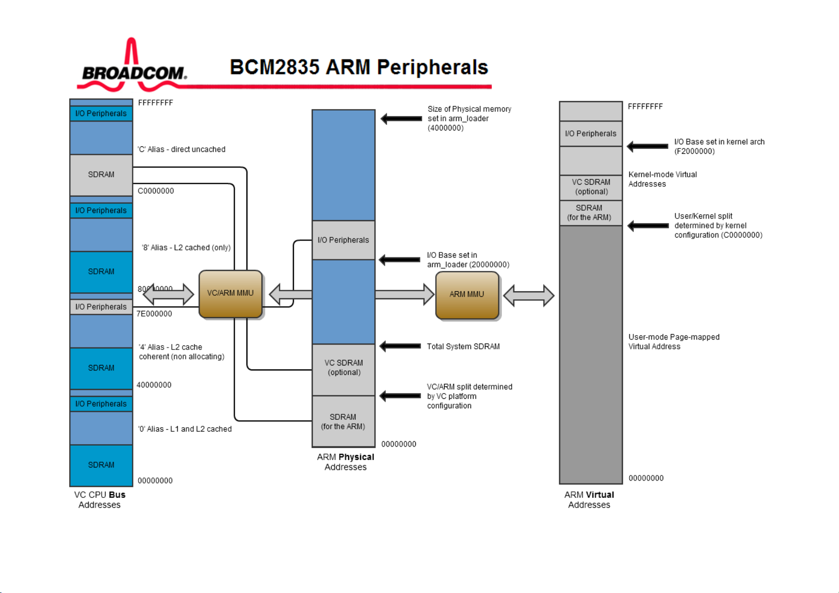
1.2.1 Diagrammatic overview
In addition to the ARM’s MMU, BCM2835 includes a second coarse-grained MMU for
mapping ARM physical addresses onto system bus addresses. This diagram shows the main
address spaces of interest:
06 February 2012 Broadcom Europe Ltd. 406 Science Park Milton Road Cambridge CB4 0WW Page 4
© 2012 Broadcom Corporation. All rights reserved
Page 5
06 February 2012 Broadcom Europe Ltd. 406 Science Park Milton Road Cambridge CB4 0WW Page 5
© 2012 Broadcom Corporation. All rights reserved
Page 6

Addresses in ARM Linux are:
• issued as virtual addresses by the ARM core, then
• mapped into a physical address by the ARM MMU, then
• mapped into a bus address by the ARM mapping MMU, and finally
• used to select the appropriate peripheral or location in RAM.
1.2.2 ARM virtual addresses (standard Linux kernel only)
As is standard practice, the standard BCM2835 Linux kernel provides a contiguous mapping
over the whole of available RAM at the top of memory. The kernel is configured for a
1GB/3GB split between kernel and user-space memory.
The split between ARM and GPU memory is selected by installing one of the supplied
start*.elf files as start.elf in the FAT32 boot partition of the SD card. The minimum amount
of memory which can be given to the GPU is 32MB, but that will restrict the multimedia
performance; for example, 32MB does not provide enough buffering for the GPU to do
1080p30 video decoding.
Virtual addresses in kernel mode will range between 0xC0000000 and 0xEFFFFFFF.
Virtual addresses in user mode (i.e. seen by processes running in ARM Linux) will range
between 0x00000000 and 0xBFFFFFFF.
Peripherals (at physical address 0x20000000 on) are mapped into the kernel virtual address
space starting at address 0xF2000000. Thus a peripheral advertised here at bus address
0x7Ennnnnn is available in the ARM kenel at virtual address 0xF2nnnnnn.
1.2.3 ARM physical addresses
Physical addresses start at 0x00000000 for RAM.
• The ARM section of the RAM starts at 0x00000000.
• The VideoCore section of the RAM is mapped in only if the system is configured to
support a memory mapped display (this is the common case).
The VideoCore MMU maps the ARM physical address space to the bus address space seen
by VideoCore (and VideoCore peripherals). The bus addresses for RAM are set up to map
onto the uncached1 bus address range on the VideoCore starting at 0xC0000000.
Physical addresses range from 0x20000000 to 0x20FFFFFF for peripherals. The bus
addresses for peripherals are set up to map onto the peripheral bus address range starting at
0x7E000000. Thus a peripheral advertised here at bus address 0x7Ennnnnn is available at
physical address 0x20nnnnnn.
1.2.4 Bus addresses
The peripheral addresses specified in this document are bus addresses. Software directly
accessing peripherals must translate these addresses into physical or virtual addresses, as
described above. Software accessing peripherals using the DMA engines must use bus
addresses.
1
BCM2835 provides a 128KB system L2 cache, which is used primarily by the GPU. Accesses to memory are
routed either via or around the L2 cache depending on senior two bits of the bus address.
06 February 2012 Broadcom Europe Ltd. 406 Science Park Milton Road Cambridge CB4 0WW Page 6
© 2012 Broadcom Corporation. All rights reserved
Page 7

Software accessing RAM directly must use physical addresses (based at 0x00000000).
Software accessing RAM using the DMA engines must use bus addresses (based at
0xC0000000).
1.3 Peripheral access precautions for correct memory ordering
The BCM2835 system uses an AMBA AXI-compatible interface structure. In order to keep
the system complexity low and data throughput high, the BCM2835 AXI system does not
always return read data in-order2. The GPU has special logic to cope with data arriving outof-order; however the ARM core does not contain such logic. Therefore some precautions
must be taken when using the ARM to access peripherals.
Accesses to the same peripheral will always arrive and return in-order. It is only when
switching from one peripheral to another that data can arrive out-of-order. The simplest way
to make sure that data is processed in-order is to place a memory barrier instruction at critical
positions in the code. You should place:
• A memory write barrier before the first write to a peripheral.
• A memory read barrier after the last read of a peripheral.
It is not required to put a memory barrier instruction after each read or write access. Only at
those places in the code where it is possible that a peripheral read or write may be followed
by a read or write of a different peripheral. This is normally at the entry and exit points of the
peripheral service code.
As interrupts can appear anywhere in the code so you should safeguard those. If an interrupt
routine reads from a peripheral the routine should start with a memory read barrier. If an
interrupt routine writes to a peripheral the routine should end with a memory write barrier.
2
Normally a processor assumes that if it executes two read operations the data will arrive in order. So a read
from location X followed by a read from location Y should return the data of location X first, followed by the
data of location Y. Data arriving out of order can have disastrous consequences. For example:
a_status = *pointer_to_peripheral_a;
b_status = *pointer_to_peripheral_b;
Without precuations the values ending up in the variables a_status and b_status can be swapped around.
It is theoretical possible for writes to go ‘wrong’ but that is far more difficult to achieve. The AXI system
makes sure the data always arrives in-order at its intended destination. So:
*pointer_to_peripheral_a = value_a;
*pointer_to_peripheral_b = value_b;
will always give the expected result. The only time write data can arrive out-of-order is if two different
peripherals are connected to the same external equipment.
06 February 2012 Broadcom Europe Ltd. 406 Science Park Milton Road Cambridge CB4 0WW Page 7
© 2012 Broadcom Corporation. All rights reserved
Page 8
2 Auxiliaries: UART1 & SPI1, SPI2
2.1 Overview
The Device has three Auxiliary peripherals: One mini UART and two SPI masters. These
three peripheral are grouped together as they share the same area in the peripheral register
map and they share a common interrupt. Also all three are controlled by the auxiliary enable
register.
Auxiliary peripherals Register Map
(offset = 0x7E21 5000)
Address Register Name3 Description Size
0x7E21 5000 AUX_IRQ Auxiliary Interrupt status 3
0x7E21 5004 AUX_ENABLES Auxiliary enables 3
0x7E21 5040 AUX_MU_IO_REG Mini Uart I/O Data 8
0x7E21 5044 AUX_MU_IER_REG Mini Uart Interrupt Enable 8
0x7E21 5048 AUX_MU_IIR_REG Mini Uart Interrupt Identify 8
0x7E21 504C AUX_MU_LCR_REG Mini Uart Line Control 8
0x7E21 5050 AUX_MU_MCR_REG Mini Uart Modem Control 8
0x7E21 5054 AUX_MU_LSR_REG Mini Uart Line Status 8
0x7E21 5058 AUX_MU_MSR_REG Mini Uart Modem Status 8
0x7E21 505C AUX_MU_SCRATCH Mini Uart Scratch 8
0x7E21 5060 AUX_MU_CNTL_REG Mini Uart Extra Control 8
0x7E21 5064 AUX_MU_STAT_REG Mini Uart Extra Status 32
0x7E21 5068 AUX_MU_BAUD_REG Mini Uart Baudrate 16
0x7E21 5080 AUX_SPI0_CNTL0_REG SPI 1 Control register 0 32
0x7E21 5084 AUX_SPI0_CNTL1_REG SPI 1 Control register 1 8
0x7E21 5088 AUX_SPI0_STAT_REG SPI 1 Status 32
0x7E21 5090 AUX_SPI0_IO_REG SPI 1 Data 32
0x7E21 5094 AUX_SPI0_PEEK_REG SPI 1 Peek 16
0x7E21 50C0 AUX_SPI1_CNTL0_REG SPI 2 Control register 0 32
0x7E21 50C4 AUX_SPI1_CNTL1_REG SPI 2 Control register 1 8
3
These register names are identical to the defines in the AUX_IO header file. For programming purposes these
names should be used wherever possible.
06 February 2012 Broadcom Europe Ltd. 406 Science Park Milton Road Cambridge CB4 0WW Page 8
© 2012 Broadcom Corporation. All rights reserved
Page 9

S
S
0x7E21 50C8 AUX_SPI1_STAT_REG SPI 2 Status 32
0x7E21 50D0 AUX_SPI1_IO_REG SPI 2 Data 32
0x7E21 50D4 AUX_SPI1_PEEK_REG SPI 2 Peek 16
2.1.1 AUX registers
There are two Auxiliary registers which control all three devices. One is the interrupt status
register, the second is the Auxiliary enable register. The Auxiliary IRQ status register can
help to hierarchically determine the source of an interrupt.
AUXIRQ Register (0x7E21 5000)
YNOPSIS
The AUXIRQ register is used to check any pending interrupts which may be asserted by
the three Auxiliary sub blocks.
Bit(s) Field Name Description Type Reset
31:3
2
1
0
Reserved, write zero, read as don’t care
SPI 2 IRQ If set the SPI 2 module has an interrupt pending. R 0
SPI 1 IRQ If set the SPI1 module has an interrupt pending. R 0
Mini UART
If set the mini UART has an interrupt pending. R 0
IRQ
AUXENB Register (0x7E21 5004)
YNOPSIS
The AUXENB register is used to enable the three modules; UART, SPI1, SPI2.
Bit(s) Field Name Description Type Reset
31:3
2
Reserved, write zero, read as don’t care
SPI2 enable If set the SPI 2 module is enabled.
R/W 0
If clear the SPI 2 module is disabled. That also
disables any SPI 2 module register access
1
SPI 1 enable If set the SPI 1 module is enabled.
R/W 0
If clear the SPI 1 module is disabled. That also
disables any SPI 1 module register access
0
Mini UART
enable
If set the mini UART is enabled. The UART will
immediately start receiving data, especially if the
R/W 0
UART1_RX line is low.
If clear the mini UART is disabled. That also disables
any mini UART register access
06 February 2012 Broadcom Europe Ltd. 406 Science Park Milton Road Cambridge CB4 0WW Page 9
© 2012 Broadcom Corporation. All rights reserved
Page 10

If the enable bits are clear you will have no access to a peripheral. You can not even read or
write the registers!
GPIO pins should be set up first the before enabling the UART. The UART core is build to
emulate 16550 behaviour. So when it is enabled any data at the inputs will immediately be
received . If the UART1_RX line is low (because the GPIO pins have not been set-up yet)
that will be seen as a start bit and the UART will start receiving 0x00-characters.
Valid stops bits are not required for the UART. (See also Implementation details). Hence
any bit status is acceptable as stop bit and is only used so there is clean timing start for the
next bit.
Looking after a reset: the baudrate will be zero and the system clock will be 250 MHz. So
only 2.5 µseconds suffice to fill the receive FIFO. The result will be that the FIFO is full and
overflowing in no time flat.
2.2 Mini UART
The mini UART is a secondary low throughput4 UART intended to be used as a console. It
needs to be enabled before it can be used. It is also recommended that the correct GPIO
function mode is selected before enabling the mini Uart.
The mini Uart has the following features:
• 7 or 8 bit operation.
• 1 start and 1 stop bit.
• No parities.
• Break generation.
• 8 symbols deep FIFOs for receive and transmit.
• SW controlled RTS, SW readable CTS.
• Auto flow control with programmable FIFO level.
• 16550 like registers.
• Baudrate derived from system clock.
This is a mini UART and it does NOT have the following capabilities:
• Break detection
• Framing errors detection.
• Parity bit
• Receive Time-out interrupt
• DCD, DSR, DTR or RI signals.
The implemented UART is not a 16650 compatible UART However as far as possible the
first 8 control and status registers are laid out like a 16550 UART. Al 16550 register bits
which are not supported can be written but will be ignored and read back as 0. All control
bits for simple UART receive/transmit operations are available.
4
The UART itself has no throughput limitations in fact it can run up to 32 Mega baud. But doing so requires
significant CPU involvement as it has shallow FIFOs and no DMA support.
06 February 2012 Broadcom Europe Ltd. 406 Science Park Milton Road Cambridge CB4 0WW Page 10
© 2012 Broadcom Corporation. All rights reserved
Page 11
S
2.2.1 Mini UART implementation details.
The UART1_CTS and UART1_RX inputs are synchronised and will take 2 system clock
cycles before they are processed.
The module does not check for any framing errors. After receiving a start bit and 8 (or 7)
data bits the receiver waits for one half bit time and then starts scanning for the next start bit.
The mini UART does not check if the stop bit is high or wait for the stop bit to appear. As a
result of this a UART1_RX input line which is continuously low (a break condition or an
error in connection or GPIO setup) causes the receiver to continuously receive 0x00
symbols.
The mini UART uses 8-times oversampling. The Baudrate can be calculated from:
__
freqclocksystem
baudrate
=
( )
regbaudrate
1_*8
+
If the system clock is 250 MHz and the baud register is zero the baudrate is 31.25 Mega
baud. (25 Mbits/sec or 3.125 Mbytes/sec). The lowest baudrate with a 250 MHz system
clock is 476 Baud.
When writing to the data register only the LS 8 bits are taken. All other bits are ignored.
When reading from the data register only the LS 8 bits are valid. All other bits are zero.
2.2.2 Mini UART register details.
AUX_MU_IO_REG Register (0x7E21 5040)
YNOPSIS
The AUX_MU_IO_REG register is primary used to write data to and read data from the
UART FIFOs.
If the DLAB bit in the line control register is set this register gives access to the LS 8 bits
of the baud rate. (Note: there is easier access to the baud rate register)
Bit(s) Field Name Description Type Reset
31:8
7:0
7:0
Reserved, write zero, read as don’t care
LS 8 bits
Baudrate
read/write,
DLAB=1
Transmit data
write,
DLAB=0
Access to the LS 8 bits of the 16-bit baudrate
register.
(Only If bit 7 of the line control register (DLAB bit)
is set)
Data written is put in the transmit FIFO (Provided it
is not full)
(Only If bit 7 of the line control register (DLAB bit)
R/W 0
W 0
is clear)
7:0
Receive data
read,
DLAB=0
Data read is taken from the receive FIFO (Provided
it is not empty)
(Only If bit 7 of the line control register (DLAB bit)
R 0
is clear)
06 February 2012 Broadcom Europe Ltd. 406 Science Park Milton Road Cambridge CB4 0WW Page 11
© 2012 Broadcom Corporation. All rights reserved
Page 12
AUX_MU_IIR_REG Register (0x7E21 5044)
S
YNOPSIS
The AUX_MU_IER_REG register is primary used to enable interrupts
If the DLAB bit in the line control register is set this register gives access to the MS 8 bits
of the baud rate. (Note: there is easier access to the baud rate register)
Bit(s) Field Name Description Type Reset
31:8
7:0
Reserved, write zero, read as don’t care
MS 8 bits
Baudrate
read/write,
Access to the MS 8 bits of the 16-bit baudrate register.
(Only If bit 7 of the line control register (DLAB bit) is
set)
R/w 0
DLAB=1
7:2
Reserved, write zero, read as don’t care
Some of these bits have functions in a 16550
compatible UART but are ignored here
1
0
Enable receive
interrupt
(DLAB=0)
Enable
transmit
interrupt
If this bit is set the interrupt line is asserted whenever
the receive FIFO holds at least 1 byte.
If this bit is clear no receive interrupts are generated.
If this bit is set the interrupt line is asserted whenever
the transmit FIFO is empty.
If this bit is clear no transmit interrupts are generated.
R 0
R 0
(DLAB=0)
06 February 2012 Broadcom Europe Ltd. 406 Science Park Milton Road Cambridge CB4 0WW Page 12
© 2012 Broadcom Corporation. All rights reserved
Page 13
AUX_MU_IER_REG Register (0x7E21 5048)
S
YNOPSIS
The AUX_MU_IIR_REG register shows the interrupt status.
It also has two FIFO enable status bits and (when writing) FIFO clear bits.
Bit(s) Field Name Description Type Reset
31:8
7:6 FIFO enables
Reserved, write zero, read as don’t care
Both bits always read as 1 as the FIFOs are always
R 11
enabled
5:4 - Always read as zero R 00
3 -
Always read as zero as the mini UART has no
R 0
timeout function
2:1 READ:
Interrupt ID
bits
WRITE:
FIFO clear
bits
On read this register shows the interrupt ID bit
00 : No interrupts
01 : Transmit holding register empty
10 : Receiver holds valid byte
11 : <Not possible>
On write:
R/W 00
Writing with bit 1 set will clear the receive FIFO
Writing with bit 2 set will clear the transmit FIFO
0
Interrupt
pending
This bit is clear whenever an interrupt is pending R 1
06 February 2012 Broadcom Europe Ltd. 406 Science Park Milton Road Cambridge CB4 0WW Page 13
© 2012 Broadcom Corporation. All rights reserved
Page 14
AUX_MU_LCR_REG Register (0x7E21 504C)
S
S
YNOPSIS
The AUX_MU_LCR_REG register controls the line data format and gives access to the
baudrate register
Bit(s) Field Name Description Type Reset
31:8
7 DLAB access
Reserved, write zero, read as don’t care
If set the first to Mini UART register give access the
R/W 0
the Baudrate register. During operation this bit must
be cleared.
6 Break
If set high the UART1_TX line is pulled low
R/W 0
continuously. If held for at least 12 bits times that will
indicate a break condition.
5:1
Reserved, write zero, read as don’t care
Some of these bits have functions in a 16550
0
compatible UART but are ignored here
0 data size If clear the UART works in 7-bit mode
R/W 0
If set the UART works in 8-bit mode
AUX_MU_MCR_REG Register (0x7E21 5050)
YNOPSIS
The AUX_MU_MCR_REG register controls the 'modem' signals.
Bit(s) Field Name Description Type Reset
31:8
7:2
Reserved, write zero, read as don’t care
Reserved, write zero, read as don’t care
Some of these bits have functions in a 16550
0
compatible UART but are ignored here
1 RTS If clear the UART1_RTS line is high
R/W 0
If set the UART1_RTS line is low
This bit is ignored if the RTS is used for auto-flow
control. See the Mini Uart Extra Control register
description)
0
Reserved, write zero, read as don’t care
This bit has a function in a 16550 compatible UART
0
but is ignored here
06 February 2012 Broadcom Europe Ltd. 406 Science Park Milton Road Cambridge CB4 0WW Page 14
© 2012 Broadcom Corporation. All rights reserved
Page 15
AUX_MU_LSR_REG Register (0x7E21 5054)
S
S
YNOPSIS
The AUX_MU_LSR_REG register shows the data status.
Bit(s) Field Name Description Type Reset
31:8
7
Reserved, write zero, read as don’t care
Reserved, write zero, read as don’t care
This bit has a function in a 16550 compatible UART
0
but is ignored here
6
5
4:2
Transmitter
idle
Transmitter
empty
This bit is set if the transmit FIFO is empty and the
transmitter is idle. (Finished shifting out the last bit).
This bit is set if the transmit FIFO can accept at least
one byte.
Reserved, write zero, read as don’t care
Some of these bits have functions in a 16550
R 1
R 0
0
compatible UART but are ignored here
1
Receiver
Overrun
This bit is set if there was a receiver overrun. That is:
one or more characters arrived whilst the receive
R/C 0
FIFO was full. The newly arrived charters have been
discarded. This bit is cleared each time this register is
read. To do a non-destructive read of this overrun bit
use the Mini Uart Extra Status register.
0 Data ready
This bit is set if the receive FIFO holds at least 1
R 0
symbol.
AUX_MU_MSR_REG Register (0x7E21 5058)
YNOPSIS
The AUX_MU_MSR_REG register shows the 'modem' status.
Bit(s) Field Name Description Type Reset
31:8
7:6
Reserved, write zero, read as don’t care
Reserved, write zero, read as don’t care
Some of these bits have functions in a 16550
0
compatible UART but are ignored here
5 CTS status
This bit is the inverse of the UART1_CTS input Thus
R 1
:
If set the UART1_CTS pin is low
If clear the UART1_CTS pin is high
3:0
Reserved, write zero, read as don’t care
Some of these bits have functions in a 16550
0
compatible UART but are ignored here
06 February 2012 Broadcom Europe Ltd. 406 Science Park Milton Road Cambridge CB4 0WW Page 15
© 2012 Broadcom Corporation. All rights reserved
Page 16
S
S
AUX_MU_SCRATCH Register (0x7E21 505C)
YNOPSIS
The AUX_MU_SCRATCH is a single byte storage.
Bit(s) Field Name Description Type Reset
31:8
7:0 Scratch
Reserved, write zero, read as don’t care
One whole byte extra on top of the 134217728
R/W 0
provided by the SDC
AUX_MU_CNTL_REG Register (0x7E21 5060)
YNOPSIS
The AUX_MU_CNTL_REG provides access to some extra useful and nice features not
found on a normal 16550 UART .
Bit(s) Field Name Description Type Reset
31:8
7
Reserved, write zero, read as don’t care
CTS assert
level
This bit allows one to invert the CTS auto flow
operation polarity.
R/W 0
If set the CTS auto flow assert level is low*
If clear the CTS auto flow assert level is high*
6
5:4
3
RTS assert
level
RTS AUTO
flow level
Enable
transmit Auto
flow-control
using CTS
This bit allows one to invert the RTS auto flow
operation polarity.
If set the RTS auto flow assert level is low*
If clear the RTS auto flow assert level is high*
These two bits specify at what receiver FIFO level the
RTS line is de-asserted in auto-flow mode.
00 : De-assert RTS when the receive FIFO has 3
empty spaces left.
01 : De-assert RTS when the receive FIFO has 2
empty spaces left.
10 : De-assert RTS when the receive FIFO has 1
empty space left.
11 : De-assert RTS when the receive FIFO has 4
empty spaces left.
If this bit is set the transmitter will stop if the CTS
line is de-asserted.
If this bit is clear the transmitter will ignore the status
of the CTS line
R/W 0
R/W 0
R/W 0
06 February 2012 Broadcom Europe Ltd. 406 Science Park Milton Road Cambridge CB4 0WW Page 16
© 2012 Broadcom Corporation. All rights reserved
Page 17
2
Enable receive
Auto flowcontrol using
RTS
If this bit is set the RTS line will de-assert if the
receive FIFO reaches it 'auto flow' level. In fact the
RTS line will behave as an RTR (Ready To Receive)
line.
If this bit is clear the RTS line is controlled by the
AUX_MU_MCR_REG register bit 1.
R/W 0
1
Transmitter
enable
If this bit is set the mini UART transmitter is enabled.
If this bit is clear the mini UART transmitter is
R/W 1
disabled
0
Receiver
enable
If this bit is set the mini UART receiver is enabled.
If this bit is clear the mini UART receiver is disabled
R/W 1
Receiver enable
If this bit is set no new symbols will be accepted by the receiver. Any symbols in progress of
reception will be finished.
Transmitter enable
If this bit is set no new symbols will be send the transmitter. Any symbols in progress of
transmission will be finished.
Auto flow control
Automatic flow control can be enabled independent for the receiver and the transmitter.
CTS auto flow control impacts the transmitter only. The transmitter will not send out new
symbols when the CTS line is de-asserted. Any symbols in progress of transmission when
the CTS line becomes de-asserted will be finished.
RTS auto flow control impacts the receiver only. In fact the name RTS for the control line is
incorrect and should be RTR (Ready to Receive). The receiver will de-asserted the RTS
(RTR) line when its receive FIFO has a number of empty spaces left. Normally 3 empty
spaces should be enough.
If looping back a mini UART using full auto flow control the logic is fast enough to allow
the RTS auto flow level of '10' (De-assert RTS when the receive FIFO has 1 empty space
left).
Auto flow polarity
To offer full flexibility the polarity of the CTS and RTS (RTR) lines can be programmed.
This should allow the mini UART to interface with any existing hardware flow control
available.
06 February 2012 Broadcom Europe Ltd. 406 Science Park Milton Road Cambridge CB4 0WW Page 17
© 2012 Broadcom Corporation. All rights reserved
Page 18
AUX_MU_STAT_REG Register (0x7E21 5064)
S
YNOPSIS
The AUX_MU_STAT_REG provides a lot of useful information about the internal status of
the mini UART not found on a normal 16550 UART.
Bit(s) Field Name Description Type Reset
31:28
27:24
Reserved, write zero, read as don’t care
Transmit
FIFO fill level
These bits shows how many symbols are stored in the
transmit FIFO
R 0
The value is in the range 0-8
23:20
19:16
Reserved, write zero, read as don’t care
Receive FIFO
fill level
These bits shows how many symbols are stored in the
receive FIFO
R 0
The value is in the range 0-8
15:10
9
Reserved, write zero, read as don’t care
Transmitter
done
This bit is set if the transmitter is idle and the transmit
FIFO is empty.
R 1
It is a logic AND of bits 2 and 8
8
Transmit
FIFO is empty
If this bit is set the transmitter FIFO is empty. Thus it
can accept 8 symbols.
R 1
7 CTS line This bit shows the status of the UART1_CTS line. R 0
6 RTS status This bit shows the status of the UART1_RTS line. R 0
5
Transmit
This is the inverse of bit 1 R 0
FIFO is full
4
Receiver
overrun
This bit is set if there was a receiver overrun. That is:
one or more characters arrived whilst the receive
R 0
FIFO was full. The newly arrived characters have
been discarded. This bit is cleared each time the
AUX_MU_LSR_REG register is read.
3
2
Transmitter is
idle
Receiver is
idle
If this bit is set the transmitter is idle.
If this bit is clear the transmitter is idle.
If this bit is set the receiver is idle.
If this bit is clear the receiver is busy.
R 1
R 1
This bit can change unless the receiver is disabled
1
Space
available
If this bit is set the mini UART transmitter FIFO can
accept at least one more symbol.
R 0
If this bit is clear the mini UART transmitter FIFO is
full
06 February 2012 Broadcom Europe Ltd. 406 Science Park Milton Road Cambridge CB4 0WW Page 18
© 2012 Broadcom Corporation. All rights reserved
Page 19
S
0
Symbol
available
If this bit is set the mini UART receive FIFO contains
at least 1 symbol
R 0
If this bit is clear the mini UART receiver FIFO is
empty
Receiver is idle
This bit is only useful if the receiver is disabled. The normal use is to disable the receiver.
Then check (or wait) until the bit is set. Now you can be sure that no new symbols will
arrive. (e.g. now you can change the baudrate...)
Transmitter is idle
This bit tells if the transmitter is idle. Note that the bit will set only for a short time if the
transmit FIFO contains data. Normally you want to use bit 9: Transmitter done.
RTS status
This bit is useful only in receive Auto flow-control mode as it shows the status of the RTS
line.
AUX_MU_BAUD Register (0x7E21 5068)
YNOPSIS
The AUX_MU_BAUD register allows direct access to the 16-bit wide baudrate counter.
Bit(s) Field Name Description Type Reset
31:16
Reserved, write zero, read as don’t care
15:0 Baudrate mini UART baudrate counter R/W 0
This is the same register as is accessed using the LABD bit and the first two register, but
much easier to access.
06 February 2012 Broadcom Europe Ltd. 406 Science Park Milton Road Cambridge CB4 0WW Page 19
© 2012 Broadcom Corporation. All rights reserved
Page 20
2.3 Universal SPI Master (2x)
The two universal SPI masters are secondary low throughput5 SPI interfaces. Like the UART
the devices needs to be enabled before they can be used. Each SPI master has the following
features:
• Single beat bit length between 1 and 32 bits.
• Single beat variable bit length between 1 and 24 bits
• Multi beat infinite bit length.
• 3 independent chip selects per master.
• 4 entries 32-bit wide transmit and receive FIFOs.
• Data out on rising or falling clock edge.
• Data in on rising or falling clock edge.
• Clock inversion (Idle high or idle low).
• Wide clocking range.
• Programmable data out hold time.
• Shift in/out MS or LS bit first
A major issue with an SPI interface is that there is no SPI standard in any form. Because the
SPI interface has been around for a long time some pseudo-standard rules have appeared
mostly when interfacing with memory devices. The universal SPI master has been developed
to work even with the most 'non-standard' SPI devices.
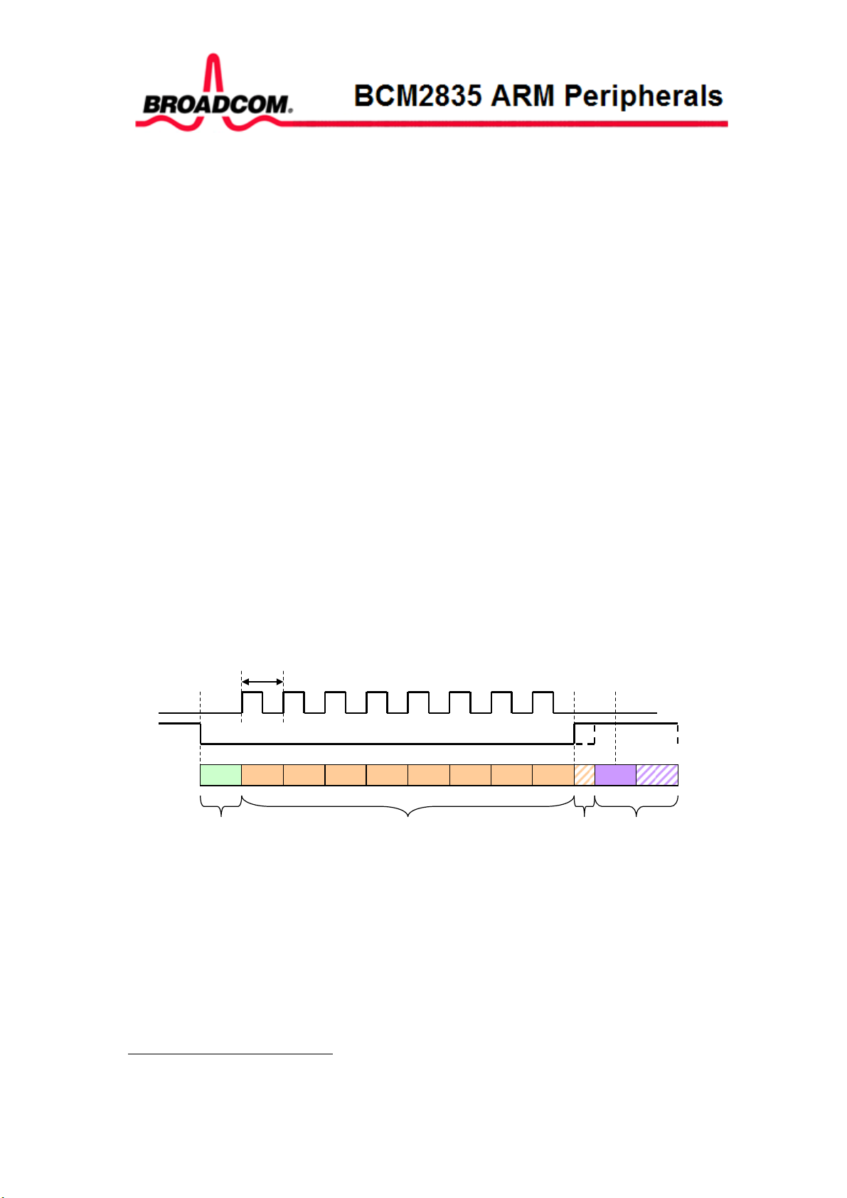
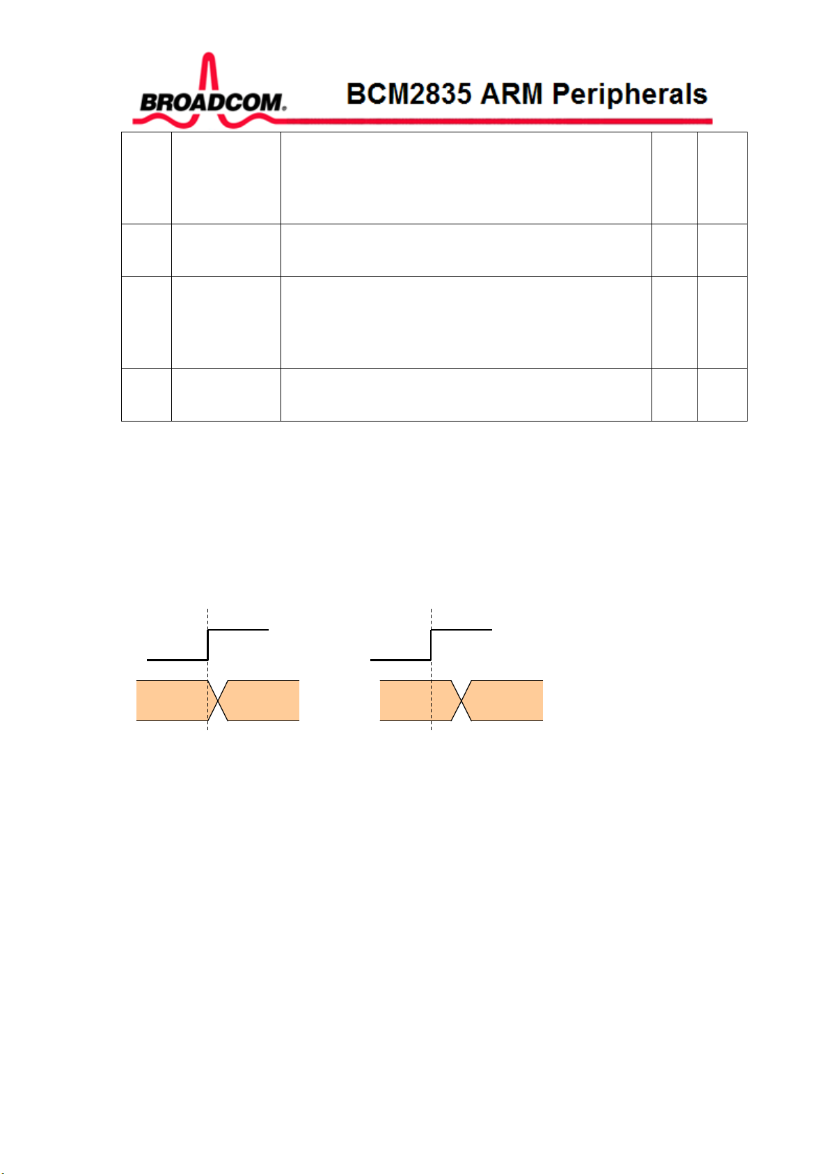
2.3.1 SPI implementation details
The following diagrams shows a typical SPI access cycle. In this case we have 8 SPI clocks.
Clk
Cs_n
1 Bit time
Set-up Operate
Hold
(optional)
Idle
One bit time before any clock edge changes the CS_n will go low. This makes sure that the
MOSI signal has a full bit-time of set-up against any changing clock edges.
The operation normally ends after the last clock cycle. Note that at the end there is one halfbit time where the clock does not change but which still is part of the operation cycle.
There is an option to add a half bit cycle hold time. This makes sure that any MISO data has
at least a full SPI bit time to arrive. (Without this hold time, data clocked out of the SPI
device on the last clock edge would have only half a bit time to arrive).
5
Again the SPIs themselves have no throughput limitations in fact they can run with an SPI clock of 125 MHz.
But doing so requires significant CPU involvement as they have shallow FIFOs and no DMA support.
06 February 2012 Broadcom Europe Ltd. 406 Science Park Milton Road Cambridge CB4 0WW Page 20
© 2012 Broadcom Corporation. All rights reserved
Page 21

Last there is a guarantee of at least a full bit time where the spi chip select is high. A longer
CS_n high period can be programmed for another 1-7 cycles.
The SPI clock frequency is:
__
freqclocksystem
_
=
CLKSPIx
fieldspeed
)1_(*2
+
If the system clock is 250 MHz and the speed field is zero the SPI clock frequency is 125
MHz. The practical SPI clock will be lower as the I/O pads can not transmit or receive
signals at such high speed. The lowest SPI clock frequency with a 250 MHz system clock is
30.5 KHz.
The hardware has an option to add hold time to the MOSI signal against the SPI clk. This is
again done using the system clock. So a 250 MHz system clock will add hold times in units
of 4 ns. Hold times of 0, 1, 4 and 7 system clock cycles can be used. (So at 250MHz an
additional hold time of 0, 4, 16 and 28 ns can be achieved). The hold time is additional to the
normal output timing as specified in the data sheet.
2.3.2 Interrupts
The SPI block has two interrupts: TX FIFO is empty, SPI is Idle.
TX FIFO is empty:
This interrupt will be asserted as soon as the last entry has been read from the transmit FIFO.
At that time the interface will still be busy shifting out that data. This also implies that the
receive FIFO will not yet contain the last received data. It is possible at that time to fill the
TX FIFO again and read the receive FIFO entries which have been received. Note that there
is no "receive FIFO full" interrupt as the number of entries received is always equal to the
number of entries transmitted.
SPI is IDLE:
This interrupt will be asserted when the transmit FIFO is empty and the SPI block has
finished all actions (including the CS-high time) By this time the receive FIFO will have all
received data as well.
2.3.3 Long bit streams
The SPI module works in bursts of maximum 32 bits. Some SPI devices require data which
is longer the 32 bits. To do this the user must make use of the two different data TX
addresses: Tx data written to one address cause the CS to remain asserted. Tx data written to
the other address cause the CS to be de-asserted at the end of the transmit cycle. So in order
to exchange 96 bits you do the following:
Write the first two data words to one address, then write the third word to the other address.
06 February 2012 Broadcom Europe Ltd. 406 Science Park Milton Road Cambridge CB4 0WW Page 21
© 2012 Broadcom Corporation. All rights reserved
Page 22
2.3.4 SPI register details.
S
AUXSPI0/1_CNTL0 Register (0x7E21 5080,0x7E21 50C0)
YNOPSIS
The AUXSPIx_CNTL0 register control many features of the SPI interfaces.
Bit(s) Field Name Description Type Reset
31:20
Speed
Sets the SPI clock speed. spi clk freq =
R/W 0
system_clock_freq/2*(speed+1)
19:17
16
15
chip selects The pattern output on the CS pins when active. R/W 111
post-input
mode
Variable CS
If set the SPI input works in post input mode.
For details see text further down
If 1 the SPI takes the CS pattern and the data from the
R/W 0
R/W 0
TX fifo
If 0 the SPI takes the CS pattern from bits 17-19 of
this register
Set this bit only if also bit 14 (variable width) is set
14
Variable width
If 1 the SPI takes the shift length and the data from
R/W 0
the TX fifo
If 0 the SPI takes the shift length from bits 0-5 of this
register
13:12
DOUT Hold
time
Controls the extra DOUT hold time in system clock
cycles.
R/W 0
00 : No extra hold time
01 : 1 system clock extra hold time
10 : 4 system clocks extra hold time
11 : 7 system clocks extra hold time
11
Enable
Enables the SPI interface. Whilst disabled the FIFOs
R/W 0
can still be written to or read from
This bit should be 1 during normal operation.
10
In rising
If 1 data is clocked in on the rising edge of the SPI
R/W 0
clock
If 0 data is clocked in on the falling edge of the SPI
clock
9
Clear FIFOs
If 1 the receive and transmit FIFOs are held in reset
R/W 0
(and thus flushed.)
This bit should be 0 during normal operation.
06 February 2012 Broadcom Europe Ltd. 406 Science Park Milton Road Cambridge CB4 0WW Page 22
© 2012 Broadcom Corporation. All rights reserved
Page 23
8
Out rising
If 1 data is clocked out on the rising edge of the SPI
clock
If 0 data is clocked out on the falling edge of the SPI
clock
R/W 0
7
6
Invert SPI
CLK
Shift out MS
bit first
If 1 the 'idle' clock line state is high.
If 0 the 'idle' clock line state is low.
If 1 the data is shifted out starting with the MS bit.
(bit 15 or bit 11)
R/W 0
R/W 0
If 0 the data is shifted out starting with the LS bit. (bit
0)
5:0 Shift length Specifies the number of bits to shift
R/W 0
This field is ignored when using 'variable shift' mode
Invert SPI CLK
Changing this bit will immediately change the polarity of the SPI clock output. It is
recommended not to do this when also the CS is active as the connected devices will see this
as a clock change.
DOUT hold time
Because the interface runs of fast silicon the MOSI hold time against the clock will be very
short. This can cause considerable problems on SPI slaves. To make it easier for the slave to
see the data the hold time of the MOSI out against the SPI clock out is programmable.
CLK
CLK
MOSI
No hold time
MOSI
With hold time
Variable width
In this mode the shift length is taken from the transmit FIFO. The transmit data bits 28:24 are
used as shift length and the data bits 23:0 are the actual transmit data. If the option 'shift MS
out first' is selected the first bit shifted out will be bit 23. The receive data will arrive as
normal.
Variable CS
This mode is used together with the variable width mode. In this mode the CS pattern is
taken from the transmit FIFO. The transmit data bits 31:29 are used as CS and the data bits
23:0 are the actual transmit data. This allows the CPU to write to different SPI devices
without having to change the CS bits. However the data length is limited to 24 bits.
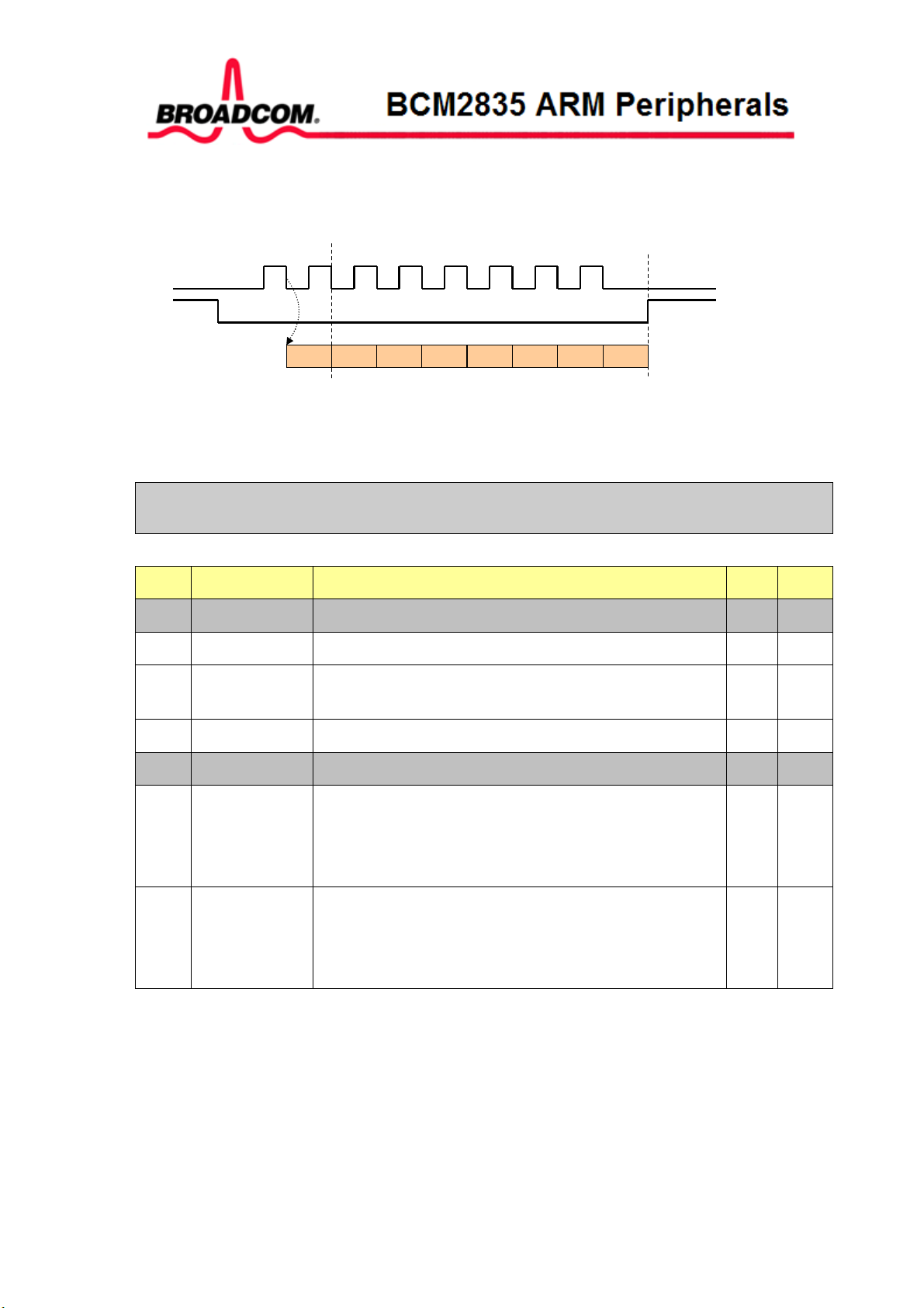
Post-input mode
Some rare SPI devices output data on the falling clock edge which then has to be picked up
on the next falling clock edge. There are two problems with this:
1. The very first falling clock edge there is no valid data arriving.
2. After the last clock edge there is one more 'dangling' bit to pick up.
06 February 2012 Broadcom Europe Ltd. 406 Science Park Milton Road Cambridge CB4 0WW Page 23
© 2012 Broadcom Corporation. All rights reserved
Page 24
S
The post-input mode is specifically to deal with this sort of data. If the post-input mode bit is
set, the data arriving at the first falling clock edge is ignored. Then after the last falling clock
edge the CS remain asserted and after a full bit time the last data bit is picked up. The
following figure shows this behaviour:
Clk
Cs_n
Get first bit Get last bit
In this mode the CS will go high 1 full SPI clock cycle after the last clock edge. This
guarantees a full SPI clock cycle time for the data to settle and arrive at the MISO input.
AUXSPI0/1_CNTL1 Register (0x7E21 5084,0x7E21 50C4)
YNOPSIS
The AUXSPIx_CNTL1 registers control more features of the SPI interfaces.
Bit(s) Field Name Description Type Reset
31:18
10:8
7
- Reserved, write zero, read as don’t care
CS high time Additional SPI clock cycles where the CS is high. R/W 0
TX empty IRQ
If 1 the interrupt line is high when the transmit FIFO
R/W 0
is empty
6
5:2
1
Done IRQ If 1 the interrupt line is high when the interface is idle R/W 0
- Reserved, write zero, read as don’t care
Shift in MS bit
first
If 1 the data is shifted in starting with the MS bit. (bit
15)
R/W 0
If 0 the data is shifted in starting with the LS bit. (bit
0)
0 Keep input
If 1 the receiver shift register is NOT cleared. Thus
R/W 0
new data is concatenated to old data.
If 0 the receiver shift register is cleared before each
transaction.
Keep input
Setting the 'Keep input' bit will make that the input shift register is not cleared between
transactions. However the contents of the shift register is still written to the receive FIFO at
the end of each transaction. E.g. if you receive two 8 bit values 0x81 followed by 0x46 the
receive FIFO will contain: 0x0081 in the first entry and 0x8146 in the second entry. This
mode may save CPU time concatenating bits (4 bits followed by 12 bits).
06 February 2012 Broadcom Europe Ltd. 406 Science Park Milton Road Cambridge CB4 0WW Page 24
© 2012 Broadcom Corporation. All rights reserved
Page 25
S
CS high time
The SPI CS will always be high for at least 1 SPI clock cycle. Some SPI devices need more
time to process the data. This field will set a longer CS-high time. So the actual CS high time
is (CS_high_time + 1) (In SPI clock cycles).
Interrupts
The SPI block has two interrupts: TX FIFO is empty, SPI is Idle.
TX FIFO is empty:
This interrupt will be asserted as soon as the last entry has been read from the transmit FIFO.
At that time the interface will still be busy shifting out that data. This also implies that the
receive FIFO will not yet contain the last received data.
It is possible at that time to fill the TX FIFO again and read the receive FIFO entries which
have been received. There is a RX FIFO level field which tells exactly how many words are
in the receive FIFO. In general at that time the receive FIFO should contain the number of
Tx items minus one (the last one still being received). Note that there is no "receive FIFO
full" interrupt or "receive FIFO overflow" flag as the number of entries received can never
be more then the number of entries transmitted.
AUX is IDLE:
This interrupt will be asserted when the module has finished all activities, including waiting
the minimum CS high time. This guarantees that any receive data will be available and
`transparent' changes can be made to the configuration register (e.g. inverting the SPI clock
polarity).
AUXSPI0/1_STAT Register (0x7E21 5088,0x7E21 50C8)
YNOPSIS
The AUXSPIx_STAT registers show the status of the SPI interfaces.
Bit(s) Field Name Description Type Reset
31:24
23:12
11:5
4
TX FIFO level The number of data units in the transmit data FIFO R/W 0
RX FIFO level The number of data units in the receive data FIFO. R/W 0
- Reserved, write zero, read as don’t care
TX Full If 1 the transmit FIFO is full
R/W 0
If 0 the transmit FIFO can accept at least 1 data unit.
3
TX Empty If 1 the transmit FIFO is empty
R/W 0
If 0 the transmit FIFO holds at least 1 data unit.
2
RX Empty If 1 the receiver FIFO is empty
R/W 0
If 0 the receiver FIFO holds at least 1 data unit.
6
Busy Indicates the module is busy transferring data. R/W 0
5:0 Bit count
The number of bits still to be processed. Starts with
R/W 0
'shift-length' and counts down.
06 February 2012 Broadcom Europe Ltd. 406 Science Park Milton Road Cambridge CB4 0WW Page 25
© 2012 Broadcom Corporation. All rights reserved
Page 26
S
S
Busy
This status bit indicates if the module is busy. It will be clear when the TX FIFO is empty
and the module has finished all activities, including waiting the minimum CS high time.
AUXSPI0/1_PEEK Register (0x7E21 508C,0x7E21 50CC)
YNOPSIS
The AUXSPIx_PEEK registers show received data of the SPI interfaces.
Bit(s) Field Name Description Type Reset
31:16
15:0 Data
- Reserved, write zero, read as don’t care
Reads from this address will show the top entry from
RO 0
the receive FIFO, but the data is not taken from the
FIFO. This provides a means of inspecting the data
but not removing it from the FIFO.
AUXSPI0/1_IO Register
(0x7E21 50A0-0x7E21 50AC
0x7E21 50E0-0x7E21 50EC)
YNOPSIS
The AUXSPIx_IO registers are the primary data port of the SPI interfaces
These four addresses all write to the same FIFO.
Writing to any of these addresses causes the SPI CS_n pins to be de-asserted at
the end of the access
Bit(s) Field Name Description Type Reset
31:16
- Reserved, write zero, read as don’t care
15:0 Data
Writes to this address range end up in the transmit
FIFO. Data is lost when writing whilst the transmit
FIFO is full.
Reads from this address will take the top entry from
the receive FIFO. Reading whilst the receive FIFO is
will return the last data received.
R/W 0
06 February 2012 Broadcom Europe Ltd. 406 Science Park Milton Road Cambridge CB4 0WW Page 26
© 2012 Broadcom Corporation. All rights reserved
Page 27
AUXSPI0/1_TXHOLD Register
S
(0x7E21 50B0-0x7E21 50BC
0x7E21 50F0-0x7E21 50FC)
YNOPSIS
The AUXSPIx_TXHOLD registers are the extended CS port of the SPI interfaces
These four addresses all write to the same FIFO.
Writing to these addresses causes the SPI CS_n pins to remain asserted at the
end of the access
Bit(s) Field Name Description Type Reset
31:16
15:0 Data
- Reserved, write zero, read as don’t care
Writes to this address range end up in the transmit
R/W 0
FIFO. Data is lost when writing whilst the transmit
FIFO is full.
Reads from this address will take the top entry from
the receive FIFO. Reading whilst the receive FIFO is
will return the last data received.
06 February 2012 Broadcom Europe Ltd. 406 Science Park Milton Road Cambridge CB4 0WW Page 27
© 2012 Broadcom Corporation. All rights reserved
Page 28
Address
C
S
DLEN
A
FIFO
DIV
DEL
3 BSC
3.1 Introduction
The Broadcom Serial Controller (BSC) controller is a master, fast-mode (400Kb/s) BSC
controller. The Broadcom Serial Control bus is a proprietary bus compliant with the Philips®
I2C bus/interface version 2.1 January 2000.
• I2C single master only operation (supports clock stretching wait states)
• Both 7-bit and 10-bit addressing is supported.
• Timing completely software controllable via registers
3.2 Register View
The BSC controller has eight memory-mapped registers. All accesses are assumed to be 32bit. Note that the BSC2 master is used dedicated with the HDMI interface and should not be
accessed by user programs.
There are three BSC masters inside BCM. The register addresses starts from
• BSC0: 0x7E20_5000
• BSC1: 0x7E80_4000
• BSC2 : 0x7E80_5000
The table below shows the address of I2C interface where the address is an offset from one of
the three base addreses listed above.
I2C Address Map
Offset
0x0
0x4
0x8
0xc
Register Name Description Size
Control 32
Status 32
Data Length 32
Slave Address 32
0x10
0x14
0x18
Data FIFO 32
Clock Divider 32
Data Delay 32
06 February 2012 Broadcom Europe Ltd. 406 Science Park Milton Road Cambridge CB4 0WW Page 28
© 2012 Broadcom Corporation. All rights reserved
Page 29
0x1c
CLKT
Synopsis
Bit(s)
Field Name
Description
Type
Reset
Reserved
-
Write as 0, read as don't care
Reserved
-
Write as 0, read as don't care
Clock Stretch Timeout 32
C Register
The control register is used to enable interrupts, clear the FIFO, define a read or write
operation and start a transfer.
The READ field specifies the type of transfer.
The CLEAR field is used to clear the FIFO. Writing to this field is a one-shot operation
which will always read back as zero. The CLEAR bit can set at the same time as the
start transfer bit, and will result in the FIFO being cleared just prior to the start of
transfer. Note that clearing the FIFO during a transfer will result in the transfer being
aborted.
The ST field starts a new BSC transfer. This has a one shot action, and so the bit will
always read back as 0 .
The INTD field enables interrupts at the end of a transfer the DONE condition. The
interrupt remains active until the DONE condition is cleared by writing a 1 to the
I2CS.DONE field. Writing a 0 to the INTD field disables interrupts on DONE.
The INTT field enables interrupts whenever the FIFO is or more empty and needs
writing (i.e. during a write transfer) - the TXW condition. The interrupt remains active
until the TXW condition is cleared by writing sufficient data to the FIFO to complete the
transfer. Writing a 0 to the INTT field disables interrupts on TXW.
The INTR field enables interrupts whenever the FIFO is or more full and needs reading
(i.e. during a read transfer) - the RXR condition. The interrupt remains active until the
RXW condition is cleared by reading sufficient data from the RX FIFO. Writing a 0 to
the INTR field disables interrupts on RXR.
The I2CEN field enables BSC operations. If this bit is 0 then transfers will not be
performed. All register accesses are still permitted however.
31:16
15 I2CEN I2C Enable
RW 0x0
0 = BSC controller is disabled
1 = BSC controller is enabled
14:11
10 INTR INTR Interrupt on RX
RW 0x0
0 = Don t generate interrupts on RXR condition.
1 = Generate interrupt while RXR = 1.
9 INTT INTT Interrupt on TX
RW 0x0
0 = Don t generate interrupts on TXW condition.
1 = Generate interrupt while TXW = 1.
06 February 2012 Broadcom Europe Ltd. 406 Science Park Milton Road Cambridge CB4 0WW Page 29
© 2012 Broadcom Corporation. All rights reserved
Page 30
8 INTD INTD Interrupt on DONE
Reserved
-
Write as 0, read as don't care
Reserved
-
Write as 0, read as don't care
0 = Don t generate interrupts on DONE
condition. 1 = Generate interrupt while DONE =
1.
RW 0x0
7 ST ST Start Transfer
0 = No action. 1 = Start a new transfer. One shot
operation. Read back as 0.
6
5:4 CLEAR CLEAR FIFO Clear
00 = No action. x1 = Clear FIFO. One shot
operation. 1x = Clear FIFO. One shot operation.
If CLEAR and ST are both set in the same
operation, the FIFO is cleared before the new
frame is started. Read back as 0.
Note: 2 bits are used to maintain compatibility to
previous version.
3:1
0 READ READ Read Transfer
0 = Write Packet Transfer. 1 = Read Packet
Transfer.
RW 0x0
RW 0x0
RW 0x0
S Register
06 February 2012 Broadcom Europe Ltd. 406 Science Park Milton Road Cambridge CB4 0WW Page 30
© 2012 Broadcom Corporation. All rights reserved
Page 31

Synopsis
Bit(s)
Field Name
Description
Type
Reset
Reserved
-
Write as 0, read as don't care
The status register is used to record activity status, errors and interrupt requests.
The TA field indicates the activity status of the BSC controller. This read-only field
returns a 1 when the controller is in the middle of a transfer and a 0 when idle.
The DONE field is set when the transfer completes. The DONE condition can be used
with I2CC.INTD to generate an interrupt on transfer completion. The DONE field is
reset by writing a 1 , writing a 0 to the field has no effect.
The read-only TXW bit is set during a write transfer and the FIFO is less than full and
needs writing. Writing sufficient data (i.e. enough data to either fill the FIFO more than
full or complete the transfer) to the FIFO will clear the field. When the I2CC.INTT
control bit is set, the TXW condition can be used to generate an interrupt to write more
data to the FIFO to complete the current transfer. If the I2C controller runs out of data
to send, it will wait for more data to be written into the FIFO.
The read-only RXR field is set during a read transfer and the FIFO is or more full and
needs reading. Reading sufficient data to bring the depth below will clear the field.
When I2CC.INTR control bit is set, the RXR condition can be used to generate an
interrupt to read data from the FIFO before it becomes full. In the event that the FIFO
does become full, all I2C operations will stall until data is removed from the FIFO.
The read-only TXD field is set when the FIFO has space for at least one byte of data.
TXD is clear when the FIFO is full. The TXD field can be used to check that the FIFO
can accept data before any is written. Any writes to a full TX FIFO will be ignored.
The read-only RXD field is set when the FIFO contains at least one byte of data. RXD
is cleared when the FIFO becomes empty. The RXD field can be used to check that
the FIFO contains data before reading. Reading from an empty FIFO will return invalid
data.
The read-only TXE field is set when the FIFO is empty. No further data will be
transmitted until more data is written to the FIFO.
The read-only RXF field is set when the FIFO is full. No more clocks will be generated
until space is available in the FIFO to receive more data.
The ERR field is set when the slave fails to acknowledge either its address or a data
byte written to it. The ERR field is reset by writing a 1 , writing a 0 to the field has no
effect.
The CLKT field is set when the slave holds the SCL signal high for too long (clock
stretching). The CLKT field is reset by writing a 1 , writing a 0 to the field has no effect.
31:10
9 CLKT CLKT Clock Stretch Timeout
RW 0x0
0 = No errors detected. 1 = Slave has held the
SCL signal low (clock stretching) for longer and
that specified in the I2CCLKT register Cleared
by writing 1 to the field.
8 ERR ERR ACK Error
RW 0x0
0 = No errors detected. 1 = Slave has not
acknowledged its address. Cleared by writing 1
to the field.
7 RXF RXF - FIFO Full
RO 0x0
0 = FIFO is not full. 1 = FIFO is full. If a read is
underway, no further serial data will be received
until data is read from FIFO.
06 February 2012 Broadcom Europe Ltd. 406 Science Park Milton Road Cambridge CB4 0WW Page 31
© 2012 Broadcom Corporation. All rights reserved
Page 32

6 TXE TXE - FIFO Empty
Synopsis
Bit(s)
Field Name
Description
Type
Reset
Reserved
-
Write as 0, read as don't care
0 = FIFO is not empty. 1 = FIFO is empty. If a
write is underway, no further serial data can be
transmitted until data is written to the FIFO.
RO 0x1
5 RXD RXD - FIFO contains Data
0 = FIFO is empty. 1 = FIFO contains at least 1
byte. Cleared by reading sufficient data from
FIFO.
4 TXD TXD - FIFO can accept Data
0 = FIFO is full. The FIFO cannot accept more
data. 1 = FIFO has space for at least 1 byte.
3 RXR RXR - FIFO needs Reading ( full)
0 = FIFO is less than full and a read is
underway. 1 = FIFO is or more full and a read is
underway. Cleared by reading sufficient data
from the FIFO.
2 TXW TXW - FIFO needs Writing ( full)
0 = FIFO is at least full and a write is underway
(or sufficient data to send). 1 = FIFO is less then
full and a write is underway. Cleared by writing
sufficient data to the FIFO.
1 DONE DONE Transfer Done
0 = Transfer not completed. 1 = Transfer
complete. Cleared by writing 1 to the field.
RO 0x0
RO 0x1
RO 0x0
RO 0x0
RW 0x0
0 TA TA Transfer Active
0 = Transfer not active. 1 = Transfer active.
DLEN Register
The data length register defines the number of bytes of data to transmit or receive in
the I2C transfer. Reading the register gives the number of bytes remaining in the
current transfer.
The DLEN field specifies the number of bytes to be transmitted/received. Reading the
DLEN field when a transfer is in progress (TA = 1) returns the number of bytes still to
be transmitted or received. Reading the DLEN field when the transfer has just
completed (DONE = 1) returns zero as there are no more bytes to transmit or receive.
Finally, reading the DLEN field when TA = 0 and DONE = 0 returns the last value
written. The DLEN field can be left over multiple transfers.
31:16
RO 0x0
06 February 2012 Broadcom Europe Ltd. 406 Science Park Milton Road Cambridge CB4 0WW Page 32
© 2012 Broadcom Corporation. All rights reserved
Page 33

15:0 DLEN Data Length.
Synopsis
Bit(s)
Field Name
Description
Type
Reset
Reserved
-
Write as 0, read as don't care
Synopsis
Bit(s)
Field Name
Description
Type
Reset
Reserved
-
Write as 0, read as don't care
Writing to DLEN specifies the number of bytes to
be transmitted/received. Reading from DLEN
when TA = 1 or DONE = 1, returns the number
of bytes still to be transmitted or received.
Reading from DLEN when TA = 0 and DONE =
0, returns the last DLEN value written. DLEN can
be left over multiple packets.
A Register
The slave address register specifies the slave address and cycle type. The address
register can be left across multiple transfers
The ADDR field specifies the slave address of the I2C device.
RW 0x0
31:7
6:0 ADDR Slave Address. RW 0x0
FIFO Register
The Data FIFO register is used to access the FIFO. Write cycles to this address place
data in the 16-byte FIFO, ready to transmit on the BSC bus. Read cycles access data
received from the bus.
Data writes to a full FIFO will be ignored and data reads from an empty FIFO will result
in invalid data. The FIFO can be cleared using the I2CC.CLEAR field.
The DATA field specifies the data to be transmitted or received.
31:8
7:0 DATA Writes to the register write transmit data to the
FIFO. Reads from register reads received data
from the FIFO.
RW 0x0
06 February 2012 Broadcom Europe Ltd. 406 Science Park Milton Road Cambridge CB4 0WW Page 33
DIV Register
© 2012 Broadcom Corporation. All rights reserved
Page 34

Synopsis
The clock divider register is used to define the clock speed of the BSC peripheral.
Bit(s)
Field Name
Description
Type
Reset
Reserved
-
Write as 0, read as don't care
Synopsis
Bit(s)
Field Name
Description
Type
Reset
The CDIV field specifies the core clock divider used by the BSC.
31:16
15:0 CDIV Clock Divider
SCL = core clock / CDIV
Where core_clk is nominally 150 MHz. If CDIV is
set to 0, the divisor is 32768. CDIV is always
rounded down to an even number. The default
value should result in a 100 kHz I2C clock
frequency.
DEL Register
The data delay register provides fine control over the sampling/launch point of the
data.
The REDL field specifies the number core clocks to wait after the rising edge before
sampling the incoming data.
The FEDL field specifies the number core clocks to wait after the falling edge before
outputting the next data bit.
Note: Care must be taken in choosing values for FEDL and REDL as it is possible to
cause the BSC master to malfunction by setting values of CDIV/2 or greater. Therefore
the delay values should always be set to less than CDIV/2.
RW 0x5dc
31:16 FEDL FEDL Falling Edge Delay
RW 0x30
Number of core clock cycles to wait after the
falling edge of SCL before outputting next bit of
data.
15:0 REDL REDL Rising Edge Delay
RW 0x30
Number of core clock cycles to wait after the
rising edge of SCL before reading the next bit of
data.
CLKT Register
06 February 2012 Broadcom Europe Ltd. 406 Science Park Milton Road Cambridge CB4 0WW Page 34
© 2012 Broadcom Corporation. All rights reserved
Page 35

Synopsis
Bit(s)
Field Name
Description
Type
Reset
Reserved
-
Write as 0, read as don't care
The clock stretch timeout register provides a timeout on how long the master waits for
the slave to stretch the clock before deciding that the slave has hung.
The TOUT field specifies the number I2C SCL clocks to wait after releasing SCL high
and finding that the SCL is still low before deciding that the slave is not responding and
moving the I2C machine forward. When a timeout occurs, the I2CS.CLKT bit is set.
Writing 0x0 to TOUT will result in the Clock Stretch Timeout being disabled.
31:16
15:0 TOUT TOUT Clock Stretch Timeout Value
Number of SCL clock cycles to wait after the
rising edge of SCL before deciding that the slave
is not responding.
RW 0x40
06 February 2012 Broadcom Europe Ltd. 406 Science Park Milton Road Cambridge CB4 0WW Page 35
© 2012 Broadcom Corporation. All rights reserved
Page 36

3.3 10 Bit Addressing
10 Bit addressing is an extension to the standard 7-bit addressing mode. This section
describes in detail how to read/write using 10-bit addressing with this I2C controller.
10-bit addressing is compatible with, and can be combined with, 7 bit addressing. Using 10
bits for addressing exploits the reserved combination 1111 0xx for the first byte following a
START (S) or REPEATED START (Sr) condition.
The 10 bit slave address is formed from the first two bytes following a S or Sr condition.
The first seven bits of the first byte are the combination 11110XX of which the last two bits
(XX) are the two most significant bits of the 10-bit address. The eighth bit of the first byte is
the R/W bit. If the R/W bit is ‘0’ (write) then the following byte contains the remaining 8 bits
of the 10-bit address. If the R/W bit is ‘1’ then the next byte contains data transmitted from
the slave to the master.
Writing
Slave acknowledge
Start
Stop
Figure 3-1 Write to a slave with 10 bit address
Figure 3-1 shows a write to a slave with a 10-bit address, to perform this using the controller
one must do the following:
Assuming we are in the ‘stop’ state: (and the FIFO is empty)
1. Write the number of data bytes to written (plus one) to the I2CDLEN register.
2. Write ‘XXXXXXXX’ to the FIFO where ‘XXXXXXXX’ are the least 8 significant bits
of the 10-bit slave address.
3. Write other data to be transmitted to the FIFO.
4. Write ‘11110XX’ to Slave Address Register where ‘XX’ are the two most significant bits
of the 10-bit address. Set I2CC.READ = 0 and I2CC.ST = 1, this will start a write transfer.
Reading
Slave acknowledge
Master acknowledge
06 February 2012 Broadcom Europe Ltd. 406 Science Park Milton Road Cambridge CB4 0WW Page 36
© 2012 Broadcom Corporation. All rights reserved
Repeat Start
Page 37

Figure 3-2 Read from slave with 10 bit address
Figure 3-2 shows how a read from a slave with a 10-bit address is performed. Following is
the procedure for performing a read using the controller:
1. Write 1 to the I2CDLEN register.
2. Write ‘XXXXXXXX’ to the FIFO where ‘XXXXXXXX’ are the least 8 significant bits
of the 10-bit slave address.
3. Write ‘11110XX’ to the Slave Address Register where ‘XX’ are the two most significant
bits of the 10-bit address. Set I2CC.READ = 0 and I2CC.ST = 1, this will start a write
transfer.
4. Poll the I2CS.TA bit, waiting for the transfer has started.
5. Write the number of data bytes to read to the I2CDLEN register.
6. Set I2CC.READ = 1 and I2CC.ST = 1, this will send the repeat start bit, new slave address
and R/W bit (which is ‘1’) initiating the read.
06 February 2012 Broadcom Europe Ltd. 406 Science Park Milton Road Cambridge CB4 0WW Page 37
© 2012 Broadcom Corporation. All rights reserved
Page 38

4 DMA Controller
4.1 Overview
The majority of hardware pipelines and peripherals within the BCM2835 are bus masters,
enabling them to efficiently satisfy their own data requirements. This reduces the
requirements of the DMA controller to block-to-block memory transfers and supporting some
of the simpler peripherals. In addition, the DMA controller provides a read only prefetch
mode to allow data to be brought into the L2 cache in anticipation of its later use.
Beware that the DMA controller is direcly connected to the peripherals. Thus the DMA
controller must be set-up to use the Physical (harware) addresses of the peripherals.
The BCM2835 DMA Controller provides a total of 16 DMA channels. Each channel operates
independently from the others and is internally arbitrated onto one of the 3 system busses.
This means that the amount of bandwidth that a DMA channel may consume can be
controlled by the arbiter settings.
Each DMA channel operates by loading a Control Block (CB) data structure from memory
into internal registers. The Control Block defines the required DMA operation. Each Control
Block can point to a further Control Block to be loaded and executed once the operation
described in the current Control Block has completed. In this way a linked list of Control
Blocks can be constructed in order to execute a sequence of DMA operations without
software intervention.
The DMA supports AXI read bursts to ensure efficient external SDRAM use. The DMA
control block contains a burst parameter which indicates the required burst size of certain
memory transfers. In general the DMA doesn’t do write bursts, although wide writes will be
done in 2 beat bursts if possible.
Memory-to-Peripheral transfers can be paced by a Data Request (DREQ) signal which is
generated by the peripheral. The DREQ signal is level sensitive and controls the DMA by
gating its AXI bus requests.
A peripheral can also provide a Panic signal alongside the DREQ to indicate that there is an
imminent danger of FIFO underflow or overflow or similar critical situation. The Panic is
used to select the AXI apriority level which is then passed out onto the AXI bus so that it can
be used to influence arbitration in the rest of the system.
The allocation of peripherals to DMA channels is programmable.
The DMA can deal with byte aligned transfers and will minimise bus traffic by buffering and
packing misaligned accesses.
Each DMA channel can be fully disabled via a top level power register to save power.
06 February 2012 Broadcom Europe Ltd. 406 Science Park Milton Road Cambridge CB4 0WW Page 38
© 2012 Broadcom Corporation. All rights reserved
Page 39

DMA Channel Offsets
DMA Channels 0
– 14 Register Set Offsets from DMA0_BASE
0x000
DMA Channel 0 Register Set
0x100
DMA Channel 1 Register Set
0x200
DMA Channel 2 Register Set
0x300
DMA Channel 3 Register Set
0x400
DMA
Channel 4 Register Set
0x500
DMA Channel 5 Register Set
0x600
DMA Channel 6 Register Set
0x700
DMA Channel 7 Register Set
0x800
DMA Channel 8 Register Set
0x900
DMA Channel 9 Register Set
0xa00
DMA Channel 10 Register Set
0xb00
DMA Channel 11
Register Set
0xc00
DMA Channel 12 Register Set
0xd00
DMA Channel 13 Register Set
0xe00
DMA Channel 14 Register Set
DMA Channel 15 Register Set Offset from DMA15_BASE
0x000
DMA Channel 15 Register Set
4.2 DMA Controller Registers
The DMA Controller is comprised of several identical DMA Channels depending upon the
required configuration. Each individual DMA channel has an identical register map (although
LITE channels have less functionality and hence less registers).
DMA Channel 0 is located at the address of 0x7E007000, Channel 1 at 0x7E007100, Channel
2 at 0x7E007200 and so on. Thus adjacent DMA Channels are offset by 0x100.
DMA Channel 15 however, is physically removed from the other DMA Channels and so has
a different address base of 0x7EE05000.
Table 4-1 – DMA Controller Register Address Map
06 February 2012 Broadcom Europe Ltd. 406 Science Park Milton Road Cambridge CB4 0WW Page 39
© 2012 Broadcom Corporation. All rights reserved
Page 40

32-bit
Associated
0 Transfer Information
TI
1 Source Address
SOURCE_AD
2 Destination Address
DEST_AD
3 Transfer Length
TXFR_LEN
4 2D Mode Stride
STRIDE
Next Control Block
6-7 Reserved
– set to zero.
N/A
4.2.1 DMA Channel Register Address Map
Each DMA channel has an identical register map, only the base address of each channel is
different.
There is a global enable register at the top of the Address map that can disable each DMA for
powersaving.
Only three registers in each channels register set are directly writeable (CS, CONBLK_AD
and DEBUG). The other registers (TI, SOURCE_AD, DEST_AD, TXFR_LEN, STRIDE &
NEXTCONBK), are automatically loaded from a Control Block data structure held in
external memory.
4.2.1.1 Control Block Data Structure
Control Blocks (CB) are 8 words (256 bits) in length and must start at a 256-bit aligned
address. The format of the CB data structure in memory, is shown below.
Each 32 bit word of the control block is automatically loaded into the corresponding 32 bit
DMA control block register at the start of a DMA transfer. The descriptions of these registers
also defines the corresponding bit locations in the CB data structure in memory.
Word
Offset Description
5
Address
Read-Only
Register
NEXTCONBK
Table 4-2 – DMA Control Block Definition
The DMA is started by writing the address of a CB structure into the CONBLK_AD register
and then setting the ACTIVE bit. The DMA will fetch the CB from the address set in the
SCB_ADDR field of this reg and it will load it into the read-only registers described below.
It will then begin a DMA transfer according to the information in the CB.
When it has completed the current DMA transfer (length => 0) the DMA will update the
CONBLK_AD register with the contents of the NEXTCONBK register, fetch a new CB from
that address, and start the whole procedure once again.
The DMA will stop (and clear the ACTIVE bit) when it has completed a DMA transfer and
the NEXTCONBK register is set to 0x0000_0000. It will load this value into the
CONBLK_AD reg and then stop.
06 February 2012 Broadcom Europe Ltd. 406 Science Park Milton Road Cambridge CB4 0WW Page 40
© 2012 Broadcom Corporation. All rights reserved
Page 41

Address
0x0
0_CS
DMA Channel 0 Control and Status
32
0x4
0_CONBLK_AD
DMA Channel 0 Control Block Address
32
0x8
0_TI
DMA Channel 0 CB Word 0 (Transfer Information)
32
0xc
0_SOURCE_AD
DMA Channel 0 CB Word 1 (Source Address)
32
0x10
0_DEST_AD
DMA Channel 0 CB Word 2 (Destination Address)
32
0x14
0_TXFR_LEN
DMA
Channel 0 CB Word 3 (Transfer Length)
32
0x18
0_STRIDE
DMA Channel 0 CB Word 4 (2D Stride)
32
0x1c
0_NEXTCONBK
DMA Channel 0 CB Word 5 (Next CB Address)
32
0x20
0_DEBUG
DMA Channel 0 Debug
32
0x100
1_CS
DMA Channel 1 Control and Status
32
0x104
1_CONBLK_AD
DMA Channel 1 Control Block Address
32
0x108
1_TI
DMA Channel 1 CB Word 0 (Transfer Information)
32
0x10c
1_SOURCE_AD
DMA Channel 1 CB Word 1 (Source Address)
32
0x110
1_DEST_AD
DMA Channel 1 CB
Word 2 (Destination Address)
32
0x114
1_TXFR_LEN
DMA Channel 1 CB Word 3 (Transfer Length)
32
Most of the control block registers cannot be written to directly as they loaded automatically
from memory. They can be read to provide status information, and to indicate the progress of
the current DMA transfer. The value loaded into the NEXTCONBK register can be
overwritten so that the linked list of Control Block data structures can be dynamically altered.
However it is only safe to do this when the DMA is paused.
4.2.1.2 Register Map
DMA Address Map
Offset
Register Name Description Size
06 February 2012 Broadcom Europe Ltd. 406 Science Park Milton Road Cambridge CB4 0WW Page 41
© 2012 Broadcom Corporation. All rights reserved
Page 42

0x118
1_STRIDE
DMA Channel 1 CB Word 4 (2D Stride)
32
0x11c
1_NEXTCONBK
DMA Channel 1 CB Word 5 (Next CB Address)
32
0x120
1_DEBUG
DMA Channel 1 Debug
32
0x200
2_CS
DMA Channel 2 Control and Status
32
0x204
2_CONBLK_AD
DMA Channel 2 Control Block Address
32
0x208
2_TI
DMA Channel 2 CB Word 0 (Transfer Information)
32
0x20c
2_SOURCE_AD
DMA Channel 2 CB Wo
rd 1 (Source Address)
32
0x210
2_DEST_AD
DMA Channel 2 CB Word 2 (Destination Address)
32
0x214
2_TXFR_LEN
DMA Channel 2 CB Word 3 (Transfer Length)
32
0x218
2_STRIDE
DMA Channel 2 CB Word 4 (2D Stride)
32
0x21c
2_NEXTCONBK
DMA Channel 2 CB Word 5 (Next CB Address)
32
0x220
2_DEBUG
DMA Channel 2 Debug
32
0x300
3_CS
DMA Channel 3 Control and Status
32
0x304
3_CONBLK_AD
DMA Channel 3 Control Block Address
32
0x308
3_TI
DMA Channel 3 CB Word 0 (Transfer
Information)
32
0x30c
3_SOURCE_AD
DMA Channel 3 CB Word 1 (Source Address)
32
0x310
3_DEST_AD
DMA Channel 3 CB Word 2 (Destination Address)
32
0x314
3_TXFR_LEN
DMA Channel 3 CB Word 3 (Transfer Length)
32
0x318
3_STRIDE
DMA Channel 3 CB Word 4 (2D Stride)
32
0x31c
3_NEXTCONBK
DMA Channel 3 CB
Word 5 (Next CB Address)
32
0x320
3_DEBUG
DMA Channel 0 Debug
32
06 February 2012 Broadcom Europe Ltd. 406 Science Park Milton Road Cambridge CB4 0WW Page 42
© 2012 Broadcom Corporation. All rights reserved
Page 43

0x400
4_CS
DMA Channel 4 Control and Status
32
0x404
4_CONBLK_AD
DMA Channel 4
Control Block Address
32
0x408
4_TI
DMA Channel 4 CB Word 0 (Transfer Information)
32
0x40c
4_SOURCE_AD
DMA Channel 4 CB Word 1 (Source Address)
32
0x410
4_DEST_AD
DMA Channel 4 CB Word 2 (Destination Address)
32
0x414
4_TXFR_LEN
DMA Channel 4 CB Word 3 (Transfer Length)
32
0x418
4_STRIDE
DMA Channel
4 CB Word 4 (2D Stride)
32
0x41c
4_NEXTCONBK
DMA Channel 4 CB Word 5 (Next CB Address)
32
0x420
4_DEBUG
DMA Channel 0 Debug
32
0x500
5_CS
DMA Channel
5 Control and Status
32
0x504
5_CONBLK_AD
DMA Channel 5 Control Block Address
32
0x508
5_TI
DMA Channel 5 CB Word 0 (Transfer Information)
32
0x50c
5_SOURCE_AD
DMA Channel 5 CB Word 1 (Source Address)
32
0x510
5_DEST_AD
DMA Channel 5 CB Word 2 (Destination Address)
32
0x514
5_TXFR_LEN
DMA
Channel 5 CB Word 3 (Transfer Length)
32
0x518
5_STRIDE
DMA Channel 5 CB Word 4 (2D Stride)
32
0x51c
5_NEXTCONBK
DMA Channel 5 CB Word 5 (Next CB Address)
32
0x520
5_DEBUG
DMA Channel 5 Debug
32
0x600
6_CS
DMA Channel 6 Control and Status
32
0x604
6_CONBLK_AD
DMA Channel 6 Control Block Address
32
0x608
6_TI
DMA Channel 6 CB Word 0 (Transfer Information)
32
06 February 2012 Broadcom Europe Ltd. 406 Science Park Milton Road Cambridge CB4 0WW Page 43
© 2012 Broadcom Corporation. All rights reserved
Page 44

0x60c
6_SOURCE_AD
DMA Channel 6 CB Word 1 (Source Address)
32
0x610
6_DEST_AD
DMA Channel 6 CB
Word 2 (Destination Address)
32
0x614
6_TXFR_LEN
DMA Channel 6 CB Word 3 (Transfer Length)
32
0x618
6_STRIDE
DMA Channel 6 CB Word 4 (2D Stride)
32
0x61c
6_NEXTCONBK
DMA Channel 6 CB Word 5 (Next CB Address)
32
0x620
6_DEBUG
DMA Channel 6 Debug
32
0x700
7_CS
DMA Channel 7 Control and Status
32
0x704
7_CONBLK_AD
DMA Channel 7 Control Block Address
32
0x708
7_TI
DMA Channel 7 CB Word 0 (Transfer Information)
32
0x70c
7_SOURCE_AD
DMA Channel 7 CB
Word 1 (Source Address)
32
0x710
7_DEST_AD
DMA Channel 7 CB Word 2 (Destination Address)
32
0x714
7_TXFR_LEN
DMA Channel 7 CB Word 3 (Transfer Length)
32
0x71c
7_NEXTCONBK
DMA Channel 7 CB Word 5 (Next CB Address)
32
0x720
7_DEBUG
DMA Channel 7 Debug
32
0x800
8_CS
DMA Channel 8 Control and Status
32
0x804
8_CONBLK_AD
DMA Channel 8 Control Block Address
32
0x808
8_TI
DMA Channel 8 CB Word 0 (Transfer Information)
32
0x80c
8_SOURCE_AD
DMA Channel 8 CB
Word 1 (Source Address)
32
0x810
8_DEST_AD
DMA Channel 8 CB Word 2 (Destination Address)
32
0x814
8_TXFR_LEN
DMA Channel 8 CB Word 3 (Transfer Length)
32
0x81c
8_NEXTCONBK
DMA Channel 8 CB Word 5 (Next CB Address)
32
06 February 2012 Broadcom Europe Ltd. 406 Science Park Milton Road Cambridge CB4 0WW Page 44
© 2012 Broadcom Corporation. All rights reserved
Page 45

0x820
8_DEBUG
DMA Channel 8 Debug
32
0x900
9_CS
DMA Channel 9 Control and Status
32
0x904
9_CONBLK_AD
DMA Channel 9 Control Block Address
32
0x908
9_TI
DMA Channel 9 CB Word 0 (Transfer Information)
32
0x90c
9_SOURCE_AD
DMA Channel 9 CB
Word 1 (Source Address)
32
0x910
9_DEST_AD
DMA Channel 9 CB Word 2 (Destination Address)
32
0x914
9_TXFR_LEN
DMA Channel 9 CB Word 3 (Transfer Length)
32
0x91c
9_NEXTCONBK
DMA Channel 9 CB Word 5 (Next CB Address)
32
0x920
9_DEBUG
DMA Channel 9 Debug
32
0xa00
10_CS
DMA Channel 10 Control and Status
32
0xa04
10_CONBLK_AD
DMA Channel 10 Control Block Address
32
0xa08
10_TI
DMA Channel 10 CB Word 0 (Transfer Information)
32
0xa0c
10_SOURCE_AD
DMA Channel
10 CB Word 1 (Source Address)
32
0xa10
10_DEST_AD
DMA Channel 10 CB Word 2 (Destination Address)
32
0xa14
10_TXFR_LEN
DMA Channel 10 CB Word 3 (Transfer Length)
32
0xa1c
10_NEXTCONBK
DMA Channel 10 CB Word 5 (Next CB Address)
32
0xa20
10_DEBUG
DMA Channel 10 Debug
32
0xb00
11_CS
DMA Channel 11 Control and Status
32
0xb04
11_CONBLK_AD
DMA Channel 11 Control Block Address
32
0xb08
11_TI
DMA Channel 11 CB Word 0 (Transfer Information)
32
0xb0c
11_SOURCE_AD
DMA
Channel 11 CB Word 1 (Source Address)
32
06 February 2012 Broadcom Europe Ltd. 406 Science Park Milton Road Cambridge CB4 0WW Page 45
© 2012 Broadcom Corporation. All rights reserved
Page 46

0xb10
11_DEST_AD
DMA Channel 11 CB Word 2 (Destination Address)
32
0xb14
11_TXFR_LEN
DMA Channel 11 CB Word 3 (Transfer Length)
32
0xb1c
11_NEXTCONBK
DMA Channel 11 CB Word 5 (Next CB Address)
32
0xb20
11_DEBUG
DMA Channel 11 Debug
32
0xc00
12_CS
DMA Channel 12 Control and Status
32
0xc04
12_CONBLK_AD
DMA Channel 12 Control Block Address
32
0xc08
12_TI
DMA Channel 12 CB Word 0 (Transfer Information)
32
0xc0c
12_SOURCE_AD
DMA Channel 12 CB Word 1 (Source Address)
32
0xc10
12_DEST_AD
DMA Channel 12 CB Word 2 (Destination Address)
32
0xc14
12_TXFR_LEN
DMA Channel 12 CB Word 3 (Transfer Length)
32
0xc1c
12_NEXTCONBK
DMA Channel 12 CB Word 5 (Next CB Address)
32
0xc20
12_DEBUG
DMA Channel 12 Debug
32
0xd00
13_CS
DMA Channel 13 Control and Statu
s 32
0xd04
13_CONBLK_AD
DMA Channel 13 Control Block Address
32
0xd08
13_TI
DMA Channel 13 CB Word 0 (Transfer Information)
32
0xd0c
13_SOURCE_AD
DMA Channel 13 CB Word 1 (Source Address)
32
0xd10
13_DEST_AD
DMA Channel 13 CB Word 2 (Destination Address)
32
0xd14
13_TXFR_LEN
DMA Channel 13 CB Word 3 (Transfer
Length)
32
0xd1c
13_NEXTCONBK
DMA Channel 13 CB Word 5 (Next CB Address)
32
0xd20
13_DEBUG
DMA Channel 13 Debug
32
0xe00
14_CS
DMA Channel 14
Control and Status
32
06 February 2012 Broadcom Europe Ltd. 406 Science Park Milton Road Cambridge CB4 0WW Page 46
© 2012 Broadcom Corporation. All rights reserved
Page 47

0xe04
14_CONBLK_AD
DMA Channel 14 Control Block Address
32
0xe08
14_TI
DMA Channel 14 CB Word 0 (Transfer Information)
32
0xe0c
14_SOURCE_AD
DMA Channel 14 CB Word 1 (Source Address)
32
0xe10
14_DEST_AD
DMA Channel 14 CB Word 2 (Destination Address)
32
0xe14
14_TXFR_LEN
DMA Channel 14 CB Word 3 (Transfer Length)
32
0xe1c
14_NEXTCONBK
DMA Channel 14 CB Word 5 (Next CB Address)
32
0xe20
14_DEBUG
DMA Channel 14 Debug
32
0xfe0
INT_STATUS
Interrupt status of each DMA channel
32
0xff0
ENABLE
Global enable bits for each DMA channel
32
Synopsis
DMA Control And Status register contains the main control and status bits for this DMA channel.
Bit(s)
Field Name
Description
Type
Reset
31 RESET
DMA Channel Reset
W1SC
0x0
30 ABORT
Abort DMA
W1SC
0x0
29 DISDEBUG
Disable debug pause
signal
RW 0x0
0_CS 1_CS 2_CS 3_CS 4_CS 5_CS 6_CS 7_CS 8_CS 9_CS 10_CS 11_CS 12_CS 13_CS 14_CS Register
Writing a 1 to this bit will reset the DMA.
The bit cannot be read, and will self
clear.
Writing a 1 to this bit will abort the
current DMA CB. The DMA will load the
next CB and attempt to continue. The bit
cannot be read, and will self clear.
When set to 1, the DMA will not stop
when the debug pause signal is asserted.
06 February 2012 Broadcom Europe Ltd. 406 Science Park Milton Road Cambridge CB4 0WW Page 47
© 2012 Broadcom Corporation. All rights reserved
Page 48

28 WAIT_FOR_OUTSTANDING_WRITES
Wait for outstanding writes
When set to 1, the DMA will keep a tally
RW 0x0
27:24 Reserved
-
Write as 0, read as don't care
23:20
PANIC_PRIORITY
AXI Panic Priority Level
RW 0x0
19:16
PRIORITY
AXI Priority Level
RW 0x0
15:9
Reserved
-
Write as 0, read as don't care
8 ERROR
DMA Error
RO 0x0
7
Reserved
-
Write as 0, read as don't care
of the AXI writes going out and the write
responses coming in. At the very end of
the current DMA transfer it will wait
until the last outstanding write response
has been received before indicating the
transfer is complete. Whilst waiting it
will load the next CB address (but will
not fetch the CB), clear the active flag (if
the next CB address = zero), and it will
defer setting the END flag or the INT flag
until the last outstanding write response
has been received.
In this mode, the DMA will pause if it has
more than 13 outstanding writes at any
one time.
Sets the priority of panicking AXI bus
transactions. This value is used when the
panic bit of the selected peripheral
channel is 1.
Zero is the lowest priority.
Sets the priority of normal AXI bus
transactions. This value is used when the
panic bit of the selected peripheral
channel is zero.
Zero is the lowest priority.
Indicates if the DMA has detected an
error. The error flags are available in the
debug register, and have to be cleared
by writing to that register.
1 = DMA channel has an error flag set.
0 = DMA channel is ok.
06 February 2012 Broadcom Europe Ltd. 406 Science Park Milton Road Cambridge CB4 0WW Page 48
© 2012 Broadcom Corporation. All rights reserved
Page 49

6 WAITING_FOR_OUTSTANDING_WRITES
DMA is Waiting for the Last Write to be
Received
RO 0x0
5 DREQ_STOPS_DMA
DMA Paused by DREQ State
RO 0x0
4 PAUSED
DMA Paused State
RO 0x0
3 DREQ
DREQ State
RO 0x0
2 INT Interrupt Status
W1C 0x0
Indicates if the DMA is currently waiting
for any outstanding writes to be
received, and is not transferring data.
1 = DMA channel is waiting.
Indicates if the DMA is currently paused
and not transferring data due to the
DREQ being inactive..
1 = DMA channel is paused.
0 = DMA channel is running.
Indicates if the DMA is currently paused
and not transferring data. This will occur
if: the active bit has been cleared, if the
DMA is currently executing wait cycles
or if the debug_pause signal has been
set by the debug block, or the number of
outstanding writes has exceeded the
max count.
1 = DMA channel is paused.
0 = DMA channel is running.
Indicates the state of the selected DREQ
(Data Request) signal, ie. the DREQ
selected by the PERMAP field of the
transfer info.
1 = Requesting data. This will only be
valid once the DMA has started and the
PERMAP field has been loaded from the
CB. It will remain valid, indicating the
selected DREQ signal, until a new CB is
loaded. If PERMAP is set to zero (unpaced transfer) then this bit will read
back as 1.
0 = No data request.
This is set when the transfer for the CB
ends and INTEN is set to 1. Once set it
must be manually cleared down, even if
the next CB has INTEN = 0.
Write 1 to clear.
06 February 2012 Broadcom Europe Ltd. 406 Science Park Milton Road Cambridge CB4 0WW Page 49
© 2012 Broadcom Corporation. All rights reserved
Page 50

1 END DMA End Flag
W1C 0x0
0 ACTIVE
Activate the DMA
RW 0x0
0_CONBLK_AD 1_CONBLK_AD 2_CONBLK_
AD 3_CONBLK_AD 4_CONBLK_AD 5_CONBLK_AD
Synopsis
DMA Control Block Address register.
Bit(s)
Field Name
Description
Type
Reset
31:0 SCB_ADDR
Control Block Address
RW 0x0
Synopsis
DMA Transfer Information.
Bit(s)
Field Name
Description
Type
Reset
Set when the transfer described by the
current control block is complete. Write
1 to clear.
This bit enables the DMA. The DMA will
start if this bit is set and the CB_ADDR is
non zero. The DMA transfer can be
paused and resumed by clearing, then
setting it again.
This bit is automatically cleared at the
end of the complete DMA transfer, ie.
after a NEXTCONBK = 0x0000_0000 has
been loaded.
6_CONBLK_AD 7_CONBLK_AD 8_CONBLK_AD 9_CONBLK_AD 10_CONBLK_AD 11_CONBLK_AD
12_CONBLK_AD 13_CONBLK_AD 14_CONBLK_AD Register
This tells the DMA where to find a Control Block
stored in memory. When the ACTIVE bit is set and this
address is non zero, the DMA will begin its transfer by
loading the contents of the addressed CB into the
relevant DMA channel registers.
At the end of the transfer this register will be updated
with the ADDR field of the NEXTCONBK control block
register. If this field is zero, the DMA will stop.
Reading this register will return the address of the
currently active CB (in the linked list of CB s). The
address must be 256 bit aligned, so the bottom 5 bits
of the address must be zero.
0_TI 1_TI 2_TI 3_TI 4_TI 5_TI 6_TI Register
06 February 2012 Broadcom Europe Ltd. 406 Science Park Milton Road Cambridge CB4 0WW Page 50
© 2012 Broadcom Corporation. All rights reserved
Page 51

31:27
Reserved
-
Write as 0, read as don't care
26 NO_WIDE_BURSTS
Don t Do wide writes as a 2 beat burst
This prevents the DMA from issuing wide writes as 2
RW 0x0
25:21
WAITS
Add Wait Cycles
RW 0x0
20:16
PERMAP
Peripheral Mapping
RW 0x0
15:12
BURST_LENGTH
Burst Transfer
Length
RW 0x0
11 SRC
_IGNORE
Ignore Reads
RW 0x0
10 SRC_DREQ
Control Source Reads with DREQ
RW 0x0
9 SRC_WIDTH
Source Transfer Width
RW 0x0
8 SRC_INC
Source Address Increment
RW 0x0
beat AXI bursts. This is an inefficient access mode, so
the default is to use the bursts.
This slows down the DMA throughput by setting the
number of dummy cycles burnt after each DMA read
or write operation is completed.
A value of 0 means that no wait cycles are to be
added.
Indicates the peripheral number (1-31) whose ready
signal shall be used to control the rate of the
transfers, and whose panic signals will be output on
the DMA AXI bus. Set to 0 for a continuous un-paced
transfer.
Indicates the burst length of the DMA transfers. The
DMA will attempt to transfer data as bursts of this
number of words. A value of zero will produce a single
transfer. Bursts are only produced for specific
conditions, see main text.
1 = Do not perform source reads. In addition,
destination writes will zero all the write strobes. This
is used for fast cache fill operations.
0 = Perform source reads..
1 = The DREQ selected by PER_MAP will gate the
source reads.
0 = DREQ has no effect.
1 = Use 128-bit source read width.
0 = Use 32-bit source read width.
1 = Source address increments after each read. The
address will increment by 4, if S_WIDTH=0 else by 32.
0 = Source address does not change.
06 February 2012 Broadcom Europe Ltd. 406 Science Park Milton Road Cambridge CB4 0WW Page 51
© 2012 Broadcom Corporation. All rights reserved
Page 52

7 DEST_IGNORE
Ignore Writes
1 = Do not perform destination writes.
RW 0x0
6 DEST_DREQ
Control Destination
Writes with DREQ
RW 0x0
5 DEST_WIDTH
Destination Transfer Width
RW 0x0
4 DEST_INC
Destination Address Increment
RW 0x0
3 WAIT_RESP
Wait for a Write Response
RW 0x0
2
Reserved
-
Write as 0, read as don't care
1 TDMODE
2D Mode
RW 0x0
0 INTEN
Interrupt Enable
RW 0x0
0_SOURCE_AD 1_SOURCE_AD 2_SOURCE_AD 3_SOURCE_AD 4_SOURCE_AD 5_SOURCE_AD
0 = Write data to destination.
1 = The DREQ selected by PERMAP will gate the
destination writes.
0 = DREQ has no effect.
1 = Use 128-bit destination write width.
0 = Use 32-bit destination write width.
1 = Destination address increments after each write
The address will increment by 4, if DEST_WIDTH=0
else by 32.
0 = Destination address does not change.
When set this makes the DMA wait until it receives
the AXI write response for each write. This ensures
that multiple writes cannot get stacked in the AXI bus
pipeline.
1= Wait for the write response to be received before
proceeding.
0 = Don t wait; continue as soon as the write data is
sent.
1 = 2D mode interpret the TXFR_LEN register as
YLENGTH number of transfers each of XLENGTH, and
add the strides to the address after each transfer.
0 = Linear mode interpret the TXFR register as a single
transfer of total length {YLENGTH ,XLENGTH}.
1 = Generate an interrupt when the transfer described
by the current Control Block completes.
0 = Do not generate an interrupt.
6_SOURCE_AD 7_SOURCE_AD 8_SOURCE_AD 9_SOURCE_AD 10_SOURCE_AD 11_SOURCE_AD
12_SOURCE_AD 13_SOURCE_AD 14_SOURCE_AD Register
06 February 2012 Broadcom Europe Ltd. 406 Science Park Milton Road Cambridge CB4 0WW Page 52
© 2012 Broadcom Corporation. All rights reserved
Page 53

Synopsis
DMA Source Address
Bit(s)
Field Name
Description
Type
Reset
31:0 S_ADDR
DMA Source Address
RW 0x0
0_DEST_AD 1_DEST_AD 2_DEST_AD 3_DEST_AD 4_DEST_AD 5_DEST_AD 6_DEST_AD
Synopsis
DMA Destination Address
Bit(s)
Field Name
Description
Type
Reset
31:0 D_ADDR
DMA Destination Address
RW 0x0
0_TXFR_LEN 1_TXFR_LEN 2_TXFR_LEN 3_TXFR_LEN 4_TXFR_LEN 5_TXFR_LEN 6_TXFR_LEN
Synopsis
DMA Transfer Length. This specifies the amount of data to be transferred in bytes.
Bit(s)
Field Name
Description
Type
Reset
31:30
Reserved
-
Write as 0, read as don't care
29:16
YLENGTH
When in 2D mode, This is the Y transfer length,
RW 0x0
15:0 XLENGTH
Transfer Length in bytes.
RW
0x0
Source address for the DMA operation. Updated by
the DMA engine as the transfer progresses.
7_DEST_AD 8_DEST_AD 9_DEST_AD 10_DEST_AD 11_DEST_AD 12_DEST_AD 13_DEST_AD
14_DEST_AD Register
Destination address for the DMA operation. Updated
by the DMA engine as the transfer progresses.
Register
In normal (non 2D) mode this specifies the amount of bytes to be transferred.
In 2D mode it is interpreted as an X and a Y length, and the DMA will perform Y transfers, each
of length X bytes and add the strides onto the addresses after each X leg of the transfer.
The length register is updated by the DMA engine as the transfer progresses, so it will indicate
the data left to transfer.
indicating how many xlength transfers are performed.
When in normal linear mode this becomes the top bits
of the XLENGTH
06 February 2012 Broadcom Europe Ltd. 406 Science Park Milton Road Cambridge CB4 0WW Page 53
© 2012 Broadcom Corporation. All rights reserved
Page 54

0_STRIDE 1_STRIDE 2_STRIDE 3_STRIDE 4_STRIDE 5_STRIDE 6_STRIDE Register
Synopsis
DMA 2D
Stride
Bit(s)
Field Name
Description
Type
Reset
31:16
D_STRIDE
Destination Stride (2D Mode)
RW 0x0
15:0 S_STRIDE
Source Stride (2D Mode)
RW 0x0
0_NEXTCONBK 1_NEXTCONBK 2_NEXTCONBK 3_NEXTCONBK 4_NEXTCONBK 5_NEXTCONBK
Synopsis
DMA Next Control Block Address
Bit(s)
Field Name
Description
Type
Reset
31:0 ADDR
Address of next CB for chained DMA operations.
RW
0x0
Synopsis
DMA Debug register.
Bit(s)
Field Name
Description
Type
Reset
31:29
Reserved
-
Write as 0, read as don't care
Signed (2 s complement) byte increment to apply to
the destination address at the end of each row in 2D
mode.
Signed (2 s complement) byte increment to apply to
the source address at the end of each row in 2D
mode.
6_NEXTCONBK 7_NEXTCONBK 8_NEXTCONBK 9_NEXTCONBK 10_NEXTCONBK 11_NEXTCONBK
12_NEXTCONBK 13_NEXTCONBK 14_NEXTCONBK Register
The value loaded into this register can be overwritten so that the linked list of Control Block data
structures can be altered. However it is only safe to do this when the DMA is paused. The
address must be 256 bit aligned and so the bottom 5 bits cannot be set and will read back as
zero.
0_DEBUG 1_DEBUG 2_DEBUG 3_DEBUG 4_DEBUG 5_DEBUG 6_DEBUG Register
06 February 2012 Broadcom Europe Ltd. 406 Science Park Milton Road Cambridge CB4 0WW Page 54
© 2012 Broadcom Corporation. All rights reserved
Page 55

28 LITE DMA Lite
Set if the DMA is a reduced performance LITE
RO 0x0
27:25
VERSION
DMA Version
RO 0x2
24:16
DMA_STATE
DMA State Machine State
RO 0x0
15:8 DMA_ID
DMA ID
RO 0x0
7:4 OUTSTANDING_WRITES
DMA Outstanding Writes Counter
RO 0x0
3
Reserved
-
Writ
e as 0, read as don't care
2 READ_ERROR
Slave Read Response Error
RW 0x0
1 FIFO_ERROR
Fifo Error
RW 0x0
0 READ_LAST_NOT_SET_ERROR
Read Last Not Set Error
RW 0x0
Synopsis
DMA Transfer Information.
Bit(s)
Field Name
Description
Type
Reset
31:26
Reserved
-
Write as 0, read as don't care
engine.
DMA version number, indicating control bit filed
changes.
Returns the value of the DMA engines state
machine for this channel.
Returns the DMA AXI ID of this DMA channel.
Returns the number of write responses that have
not yet been received.
This count is reset at the start of each new DMA
transfer or with a DMA reset.
Set if the read operation returned an error value on
the read response bus. It can be cleared by writing
a 1,
Set if the optional read Fifo records an error
condition. It can be cleared by writing a 1,
If the AXI read last signal was not set when
expected, then this error bit will be set. It can be
cleared by writing a 1.
7_TI 8_TI 9_TI 10_TI 11_TI 12_TI 13_TI 14_TI Register
06 February 2012 Broadcom Europe Ltd. 406 Science Park Milton Road Cambridge CB4 0WW Page 55
© 2012 Broadcom Corporation. All rights reserved
Page 56

25:21
WAITS
Add Wait Cycles
This slows down the DMA throughput by setting the
RW 0x0
20:16
PERMAP
Peripheral Mapping
RW 0x0
15:12
BURST_LENGTH
Burst Transfer Length
RW 0x0
11 SRC_IGNORE
RW 0x0
10 SRC_DREQ
Control Source Reads with DREQ
RW 0x0
9 SRC_WIDTH
Source Transfer Width
RW 0x0
8 SRC_INC
Source Address Increment
RW 0x0
7 DEST_IGNORE
RW 0x0
6 DEST_DREQ
Control Destination Writes with DREQ
RW 0x0
5 DEST_WIDTH
Destination Transfer Width
RW 0x0
number of dummy cycles burnt after each DMA read
or write operation is completed.
A value of 0 means that no wait cycles are to be
added.
Indicates the peripheral number (1-31) whose ready
signal shall be used to control the rate of the
transfers, and whose panic signals will be output on
the DMA AXI bus. Set to 0 for a continuous un-paced
transfer.
Indicates the burst length of the DMA transfers. The
DMA will attempt to transfer data as bursts of this
number of words. A value of zero will produce a single
transfer. Bursts are only produced for specific
conditions, see main text.
1 = The DREQ selected by PER_MAP will gate the
source reads.
0 = DREQ has no effect.
1 = Use 128-bit source read width.
0 = Use 32-bit source read width.
1 = Source address increments after each read. The
address will increment by 4, if S_WIDTH=0 else by 32.
0 = Source address does not change.
1 = The DREQ selected by PERMAP will gate the
destination writes.
0 = DREQ has no effect.
1 = Use 128-bit destination write width.
0 = Use 32-bit destination write width.
06 February 2012 Broadcom Europe Ltd. 406 Science Park Milton Road Cambridge CB4 0WW Page 56
© 2012 Broadcom Corporation. All rights reserved
Page 57

4 DEST_INC
Destination Address Increment
1 = Destination address increments after each write
RW 0x0
3 WAIT_RESP
Wait for a Write Response
RW 0x0
2:1
Reserved
-
Write as 0, read as don't care
0 INTEN
Interrupt Enable
RW 0x0
7_TXFR_LEN 8_TXFR_LEN 9_TXFR_LEN 10_TXFR_LEN 11_TXFR_LEN 12_TXFR_LEN 13_TXFR_LEN
Synopsis
DMA Transfer Length
Bit(s)
Field Name
Description
Type
Reset
31:16
Reserved
-
Write as 0, read as don't care
15:0 XLENGTH
Transfer Length
RW 0x0
Synopsis
DMA Lite Debug register.
Bit(s)
Field Name
Description
Type
Reset
The address will increment by 4, if DEST_WIDTH=0
else by 32.
0 = Destination address does not change.
When set this makes the DMA wait until it receives
the AXI write response for each write. This ensures
that multiple writes cannot get stacked in the AXI bus
pipeline.
1= Wait for the write response to be received before
proceeding.
0 = Don t wait; continue as soon as the write data is
sent.
1 = Generate an interrupt when the transfer described
by the current Control Block completes.
0 = Do not generate an interrupt.
14_TXFR_LEN Register
Length of transfer, in bytes. Updated by the DMA
engine as the transfer progresses.
7_DEBUG 8_DEBUG 9_DEBUG 10_DEBUG 11_DEBUG 12_DEBUG 13_DEBUG 14_DEBUG Register
06 February 2012 Broadcom Europe Ltd. 406 Science Park Milton Road Cambridge CB4 0WW Page 57
© 2012 Broadcom Corporation. All rights reserved
Page 58

31:29
Reserved
-
Write as 0, read as don't care
28 LITE DMA Lite
Set if the DMA is a reduced performance LITE
RO 0x1
27:25
VERSION
DMA Version
RO 0x2
24:16
DMA_STATE
DMA State Machine State
RO 0x0
15:8 DMA_ID
DMA ID
RO 0x0
7:4 OUTSTANDING_WRITES
DMA Outstanding Writes Counter
RO 0x0
3
Reserved
-
Write as 0, read as don't care
2 READ_ERROR
Slave Read Response Error
RW 0x0
1 FIFO_ERROR
Fifo Error
RW 0x0
0 READ_LAST_NOT_SET_ERROR
Read Last Not Set Error
RW 0x0
Synopsis
Interrupt status of each DMA engine
Bit(s)
Field Name
Description
Type
Reset
engine.
DMA version number, indicating control bit filed
changes.
Returns the value of the DMA engines state
machine for this channel.
Returns the DMA AXI ID of this DMA channel.
Returns the number of write responses that have
not yet been received.
This count is reset at the start of each new DMA
transfer or with a DMA reset.
Set if the read operation returned an error value on
the read response bus. It can be cleared by writing
a 1,
Set if the optional read Fifo records an error
condition. It can be cleared by writing a 1,
If the AXI read last signal was not set when
expected, then this error bit will be set. It can be
cleared by writing a 1.
INT_STATUS Register
06 February 2012 Broadcom Europe Ltd. 406 Science Park Milton Road Cambridge CB4 0WW Page 58
© 2012 Broadcom Corporation. All rights reserved
Page 59

31:16
Reserved
-
Write as 0, read as don't care
15 INT15
Interrupt status of DMA engine 15
RW
0x0
14 INT14
Interrupt status of
DMA engine 14
RW
0x0
13 INT13
Interrupt status of DMA engine 13
RW
0x0
12 INT12
Interrupt status of DMA engine 12
RW
0x0
11 INT11
Interrupt status of DMA engine 11
RW
0x0
10 INT10
Interrupt status of DMA engine 10
RW
0x0
9 INT9 Interrupt status of
DMA engine 9
RW
0x0
8 INT8 Interrupt status of DMA engine 8
RW
0x0
7 INT7 Interrupt status of DMA engine 7
RW
0x0
6 INT6 Interrupt status of DMA engine 6
RW
0x0
5 INT5 Interrupt status of DMA engine 5
RW
0x0
4 INT4 Interrupt status of DMA engine 4
RW
0x0
3 INT3 Interrupt status of DMA engine 3
RW
0x0
2 INT2 Interrupt status of DMA engine 2
RW
0x0
1 INT1 Interrupt status of DMA engine 1
RW
0x0
0 INT0 Interrupt status of DMA engine 0
RW
0x0
Synopsis
Global enable bits for each
channel
Bit(s)
Field Name
Description
Type
Reset
31:15
Reserved
-
Write as 0, read as don't care
06 February 2012 Broadcom Europe Ltd. 406 Science Park Milton Road Cambridge CB4 0WW Page 59
ENABLE Register
© 2012 Broadcom Corporation. All rights reserved
Page 60

14 EN14
enable dma engine 14
RW
0x1
13 EN13
enable dma engine 13
RW
0x1
12 EN12
enable dma engine 12
RW
0x1
11 EN11
enable dma engine 11
RW
0x1
10 EN10
enable dma engine 10
RW
0x1
9 EN9 enable dma engine 9
RW
0x1
8 EN8 enable dma engine 8
RW
0x1
7 EN7 enable dma engine 7
RW
0x1
6 EN6 enable dma engine 6
RW
0x1
5 EN5 enable dma engine 5
RW
0x1
4 EN4 enable dma engine 4
RW
0x1
3 EN3 enable dma
engine 3
RW
0x1
2 EN2 enable dma engine 2
RW
0x1
1 EN1 enable dma engine 1
RW
0x1
0 EN0 enable dma engine 0
RW
0x1
06 February 2012 Broadcom Europe Ltd. 406 Science Park Milton Road Cambridge CB4 0WW Page 60
© 2012 Broadcom Corporation. All rights reserved
Page 61

DREQ
Peripheral
DREQ = 1
1 DSI
2 PCM TX
3 PCM RX
4 SMI
5 PWM
6 SPI TX
7 SPI RX
4.2.1.3 Peripheral DREQ Signals
A DREQ (Data Request) mechanism is used to pace the data flow between the DMA and a
peripheral.
Each peripheral is allocated a permanent DREQ signal. Each DMA channel can select which
of the DREQ signals should be used to pace the transfer by controlling the DMA reads, DMA
writes or both. Note that DREQ 0 is permanently enabled and can be used if no DREQ is
required.
When a DREQ signal is being used to pace the DMA reads, the DMA will wait until it has
sampled DREQ high before launching a single or burst read operation. It will then wait for all
the read data to be returned before re-checking the DREQ and starting the next read. Thus
once a peripheral receives the read request it should remove its DREQ as soon as possible to
prevent the DMA from re-sampling the same DREQ assertion.
DREQ’s are not required when reading from AXI peripherals. In this case, the DMA will
request data from the peripheral and the peripheral will only send the data when it is
available. The DMA will not request data that is does not have room for, so no pacing of the
data flow is required.
DREQ’s are required when reading from APB peripherals as the AXI-to-APB bridge will not
wait for an APB peripheral to be ready and will just perfom the APB read regardless. Thus
an APB peripheral needs to make sure that it has all of its read data ready before it drives its
DREQ high.
When writing to peripherals, a DREQ is always required to pace the data. However, due to
the pipelined nature of the AXI bus system, several writes may be in flight before the
peripheral receives any data and withdraws its DREQ signal. Thus the peripheral must
ensure that it has sufficient room in its input FIFO to accommodate the maximum amount of
data that it might receive. If the peripheral is unable to do this, the DMA WAIT_RESP
mechanism can be used to ensure that only one write is in flight at any one time, however this
is less efficient transfer mechanism.
The mapping of peripherals to DREQ’s is as follows:
0
This is always on so use this
channel if no DREQ is required.
06 February 2012 Broadcom Europe Ltd. 406 Science Park Milton Road Cambridge CB4 0WW Page 61
© 2012 Broadcom Corporation. All rights reserved
Page 62

8 BSC/SPI Slave TX
9 BSC/SPI Slave RX
10 unused
11 e.MMC
12 UART TX
13 SD HOST
14 UART RX.
15 DSI
16 SLIMBUS MCTX.
17 HDMI
18 SLIMBUS MCRX
19 SLIMBUS DC0
20 SLIMBUS DC1
21 SLIMBUS DC2
22 SLIMBUS DC3
23 SLIMBUS DC4
24 Scaler FIFO 0 & SMI *
25 Scaler FIFO 1 & SMI *
26 Scaler FIFO 2 & SMI *
27 SLIMBUS DC5
28 SLIMBUS DC6
29 SLIMBUS DC7
30 SLIMBUS DC8
31 SLIMBUS DC9
* The SMI element of the Scaler FIFO 0 & SMI DREQs can be disabled by setting the
SMI_DISABLE bit in the DMA_DREQ_CONTROL register in the system arbiter control
block.
06 February 2012 Broadcom Europe Ltd. 406 Science Park Milton Road Cambridge CB4 0WW Page 62
© 2012 Broadcom Corporation. All rights reserved
Page 63

4.3 AXI Bursts
The DMA supports bursts under specific conditions. Up to 16 beat bursts can be
accommodated.
Peripheral (32 bit wide) read bursts are supported. The DMA will generate the burst if there
is sufficient room in its read buffer to accommodate all the data from the burst. This limits the
burst size to a maximum of 8 beats.
Read bursts in destination ignore mode (DEST_IGNORE) are supported as there is no need
for the DMA to deal with the data. This allows wide bursts of up to 16 beats to be used for
efficient L2 cache fills.
DMA channel 0 and 15 are fitted with an external 128 bit 8 word read FIFO. This enables
efficient memory to memory transfers to be performed. This FIFO allows the DMA to
accommodate a wide read burst up to the size of the FIFO. In practice this will allow a 128
bit wide read burst of 9 as the first word back will be immediately read into the DMA engine
(or a 32 bit peripheral read burst of 16 – 8 in the input buffer and 8 in the fifo). On any DMA
channel, if a read burst is selected that is too large, the AXI read bus will be stalled until the
DMA has written out the data. This may lead to inefficient system operation, and possibly
AXI lock up if it causes a circular dependancy.
In general write bursts are not supported. However to increase the efficiency of L2 cache
fills, src_ignore (SRC_IGNORE) transfers can be specified with a write burst. In this case
the DMA will issue a write burst address sequence followed by the appropriate number o f
zero data, zero strobe write bus cycles, which will cause the cache to pre-fetch the data. To
improve the efficiency of the 128 bit wide bus architecture, and to make use of the DMAs
internal 256 bit registers, the DMA will generate 128 bit wide writes as 2 beat bursts
wherever possible, although this behaviour can be disabled.
4.4 Error Handling
If the DMA detects a Read Response error it will record the fact in the READ_ERROR flag
in the debug register. This will remain set until it is cleared by writing a 1 to it. The DMA
will clear its active flag and generate an interrupt. Any outstanding read data transactions
(remainder of a burst) will be honoured. This allows the operator to either restart the DMA
by clearing the error bit and setting the active bit, or to abort the DMA transfer by clearing
the NEXTCONBK register and restarting the DMA with the ABORT bit set.
The DMA will also record any errors from an external read FIFO. These will be latched in
the FIFO_ERROR bit in the debug register until they are cleared by writing a ‘1’ to the bit.
(note that only DMA0 and 15 have an external read fifo)
If the DMA detects that a read occurred without the AXI rlast set as expected then it will set
the READ_LAST_NOT_SET_ERROR bit in the debug register. This can be cleared by
writing a ‘1’ to it.
The error bits are logically OR’d together and presented as a general ERROR bit in the CS
register.
4.5 DMA LITE Engines
Several of the DMA engines are of the LITE design. This is a reduced specification engine
designed to save space. The engine behaves in the same way as a normal DMA engine
except for the following differences.
06 February 2012 Broadcom Europe Ltd. 406 Science Park Milton Road Cambridge CB4 0WW Page 63
© 2012 Broadcom Corporation. All rights reserved
Page 64

1. The internal data structure is 128 bits instead of 256 bits. This means that if you do
a 128 bit wide read burst of more than 1 beat, the DMA input register will be full
and the read bus will be stalled. The normal DMA engine can accept a read burst of
2 without stalling. If you do a narrow 32 bit read burst from the peripherals then
the lite engine can cope with a burst of 4 as opposed to a burst of 8 for the normal
engine. Note that stalling the read bus will potentially reduce the overall system
performance, and may possible cause a system lockup if you end up with a conflict
where the DMA cannot free the read bus as the read stall has prevented it writing
out its data due to some circular system relationship.
2. The Lite engine does not support 2D transfers. The TDMODE, S_STRIDE,
D_STRIDE and YLENGTH registers will all be removed. Setting these registers
will have no effect.
3. The DMA length register is now 16 bits, limiting the maximum transferrable length
to 65536 bytes.
4. Source ignore (SRC_IGNORE) and destination ignore (DEST_IGNORE) modes
are removed.
The Lite engine will have about half the bandwidth of a normal DMA engine, and are
intended for low bandwith peripheral servicing.
06 February 2012 Broadcom Europe Ltd. 406 Science Park Milton Road Cambridge CB4 0WW Page 64
© 2012 Broadcom Corporation. All rights reserved
Page 65

5 External Mass Media Controller
o Introduction
The External Mass Media Controller (EMMC) is an embedded MultiMedia™ and SD™ card
interface provided by Arasan™. It is compliant to the following standards:
• SD™ Host Controller Standard Specification Version 3.0 Draft 1.0
• SDIO™ card specification version 3.0
• SD™ Memory Card Specification Draft version 3.0
• SD™ Memory Card Security Specification version 1.01
• MMC™ Specification version 3.31,4.2 and 4.4
For convenience in the following text card is used as a placeholder for SD™, embedded
MultiMedia and SDIO™ cards.
For detailed information about the EMMC internals please refer to the Arasan™ document
SD3.0_Host_AHB_eMMC4.4_Usersguide_ver5.9_jan11_10.pdf but make sure to read the
following chapter which lists the changes made to Arasan™’s IP.
Because the EMMC module shares pins with other functionality it must be selected in the
GPIO interface. Please refer to the GPIO section for further details.
The interface to the card uses its own clock clk_emmc which is provided by the clock
manager module. The frequency of this clock should be selected between 50 MHz and 100
MHz. Having a separate clock allows high performance access to the card even if the
VideoCore runs at a reduced clock frequency. The EMMC module contains its own internal
clock divider to generate the card’s clock from clk_emmc.
Additionally can the sampling clock for the response and data from the card be delayed in up
to 40 steps with a configurable delay between 200ps to 1100ps per step typically. The delay
is intended to cancel the internal delay inside the card (up to 14ns) when reading. The delay
per step will vary with temperature and supply voltage. Therefore it is better to use a bigger
delay than necessary as there is no restriction for the maximum delay.
The EMMC module handles the handshaking process on the command and data lines and all
CRC processing automatically.
Command execution is commenced by writing the command plus the appropriate flags to the
CMDTM register after loading any required argument into the ARG1 register. The EMMC
module calculates the CRC checksum, transfers the command to the card, receives the
response and checks its CRC. Once the command has executed or timed-out bit 0 of register
INTERRUPT will be set. Please note that the INTERRUPT register is not self clearing, so the
software has first to reset it by writing 1 before using it to detect if a command has finished.
06 February 2012 Broadcom Europe Ltd. 406 Science Park Milton Road Cambridge CB4 0WW Page 65
© 2012 Broadcom Corporation. All rights reserved
Page 66

Address
ARG2
BLKSIZECNT
ARG1
C
MDTM
RESP0
RESP1
The software is responsible for checking the status bits of the card’s response in order to
verify successful processing by the card.
In order to transfer data from/to the card register DATA is accessed after configuring the host
and sending the according commands to the card using CMDTM. Because the EMMC
module doesn’t interpret the commands sent to the card it is important to configure it
identical to the card setup using the CONTROL0 register. Especial care should be taken to
make sure that the width of the data bus is configured identical for host and card. The card is
synchronized to the data flow by switching off its clock appropriately. A handshake signal
dma_req is available for paced data transfers. Bit 1 of the INTERRUPT register can used to
determine whether a data transfer has finished. Please note that the INTERRUPT register is
not self clearing, so the software has first to reset it by writing 1 before using it to detect if a
data transfer has finished.
The EMMC module restricts the maximum block size to the size of the internal data FIFO
which is 1k bytes. In order to get maximum performance for data transfers it is necessary to
use multiple block data transfers. In this case the EMMC module uses two FIFOs in pingpong mode, i.e. one is used to transfer data to/from the card while the other is simultaneously
accessed by DMA via the AXI bus. If the EMMC module is configured for single block
transfers only one FIFO is used, so no DMA access is possible while data is transferred
to/from the card and vice versa resulting in long dead times.
o Registers
Contrary to Arasan™’s documentation the EMMC module registers can only be accessed as
32 bit registers, i.e. the two LSBs of the address are always zero.
The EMMC register base address is 0x7E300000
EMMC Address Map
Offset
0x0
0x4
0x8
0xc
Register Name Description Size
ACMD23 Argument 32
Block Size and Count 32
Argument 32
Command and Transfer Mode 32
0x10
0x14
Response bits 31 : 0 32
Response bits 63 : 32 32
06 February 2012 Broadcom Europe Ltd. 406 Science Park Milton Road Cambridge CB4 0WW Page 66
© 2012 Broadcom Corporation. All rights reserved
Page 67

0x18
RESP2
RESP3
DATA
STATUS
CONTROL0
CONTROL1
INTERRUPT
IRPT_MASK
IRPT_EN
CONTROL2
FORCE_IRPT
BOOT_TIMEOUT
DBG_SEL
EXRDFIFO_CFG
EXRDFIFO_EN
TUNE_STEP
TUNE_STEPS_STD
TUNE_STEPS_DDR
SPI_INT_SPT
SLOTISR_VER
Response bits 95 : 64 32
0x1c
0x20
0x24
0x28
0x2c
0x30
0x34
0x38
0x3c
0x50
Response bits 127 : 96 32
Data 32
Status 32
Host Configuration bits 32
Host Configuration bits 32
Interrupt Flags 32
Interrupt Flag Enable 32
Interrupt Generation Enable 32
Host Configuration bits 32
Force Interrupt Event 32
0x70
0x74
0x80
0x84
0x88
0x8c
0x90
0xf0
0xfc
Timeout in boot mode 32
Debug Bus Configuration 32
Extension FIFO Configuration 32
Extension FIFO Enable 32
Delay per card clock tuning step 32
Card clock tuning steps for SDR 32
Card clock tuning steps for DDR 32
SPI Interrupt Support 32
Slot Interrupt Status and Version 32
ARG2 Register
06 February 2012 Broadcom Europe Ltd. 406 Science Park Milton Road Cambridge CB4 0WW Page 67
© 2012 Broadcom Corporation. All rights reserved
Page 68

Synopsis
Bit(s)
Field Name
Description
Type
Reset
Synopsis
Bit(s)
Field Name
Description
Type
Reset
Reserved
-
Write as 0, read as don't care
Synopsis
Bit(s)
Field Name
Description
Type
Reset
This register contains the argument for the SD card specific command ACMD23
(SET_WR_BLK_ERASE_COUNT). ARG2 must be set before the ACMD23 command
is issued using the CMDTM register.
31:0 ARGUMENT Argument to be issued with ACMD23 RW 0x0
BLKSIZECNT Register
This register must not be accessed or modified while any data transfer between card
and host is ongoing.
It contains the number and size in bytes for data blocks to be transferred. Please note
that the EMMC module restricts the maximum block size to the size of the internal data
FIFO which is 1k bytes.
BLKCNT is used to tell the host how many blocks of data are to be transferred. Once
the data transfer has started and the TM_BLKCNT_EN bit in the CMDTM register is
set the EMMC module automatically decreases the BNTCNT value as the data blocks
are transferred and stops the transfer once BLKCNT reaches 0.
31:16 BLKCNT Number of blocks to be transferred RW 0x0
15:10
9:0 BLKSIZE Block size in bytes RW 0x0
ARG1 Register
This register contains the arguments for all commands except for the SD card specific
command ACMD23 which uses ARG2. ARG1 must be set before the command is
issued using the CMDTM register.
31:0 ARGUMENT Argument to be issued with command RW 0x0
06 February 2012 Broadcom Europe Ltd. 406 Science Park Milton Road Cambridge CB4 0WW Page 68
© 2012 Broadcom Corporation. All rights reserved
Page 69

Synopsis
Bit(s)
Field Name
Description
Type
Reset
Reserved
-
Write as 0, read as don't care
Reserved
-
Write as 0, read as don't care
CMDTM Register
This register is used to issue commands to the card. Besides the command it also
contains flags informing the EMMC module what card response and type of data
transfer to expect. Incorrect flags will result in strange behaviour.
For data transfers two modes are supported: either transferring a single block of data
or several blocks of the same size. The SD card uses two different sets of commands
to differentiate between them but the host needs to be additionally configured using
TM_MULTI_BLOCK. It is important that this bit is set correct for the command sent to
the card, i.e. 1 for CMD18 and CMD25 and 0 for CMD17 and CMD24. Multiple block
transfer gives a better performance.
The BLKSIZECNT register is used to configure the size and number of blocks to be
transferred. If bit TM_BLKCNT_EN of this register is set the transfer stops
automatically after the number of data blocks configured in the BLKSIZECNT register
has been transferred.
The TM_AUTO_CMD_EN bits can be used to make the host to send automatically a
command to the card telling it that the data transfer has finished once the BLKCNT bits
in the BLKSIZECNT register are 0.
31:30
29:24 CMD_INDEX Index of the command to be issued to the card RW 0x0
23:22 CMD_TYPE Type of command to be issued to the card:
RW 0x0
00 = normal
01 = suspend (the current data transfer)
10 = resume (the last data transfer)
11 = abort (the current data transfer)
21 CMD_ISDATA Command involves data transfer:
RW 0x0
0 = no data transfer command
1 = data transfer command
20 CMD_IXCHK_EN Check that response has same index as
RW 0x0
command:
0 = disabled
1 = enabled
19 CMD_CRCCHK_EN Check the responses CRC:
RW 0x0
0 = disabled
1 = enabled
18
17:16 CMD_RSPNS_TYPE Type of expected response from card:
06 February 2012 Broadcom Europe Ltd. 406 Science Park Milton Road Cambridge CB4 0WW Page 69
RW 0x0
00 = no response
01 = 136 bits response
10 = 48 bits response
11 = 48 bits response using busy
© 2012 Broadcom Corporation. All rights reserved
Page 70

15:6
Reserved
-
Write as 0, read as don't care
Reserved
-
Write as 0, read as don't care
Synopsis
Bit(s)
Field Name
Description
Type
Reset
Synopsis
5 TM_MULTI_BLOCK Type of data transfer
0 = single block
1 = multiple block
4 TM_DAT_DIR Direction of data transfer:
0 = from host to card
1 = from card to host
3:2 TM_AUTO_CMD_EN Select the command to be send after completion
of a data transfer:
00 = no command
01 = command CMD12
10 = command CMD23
11 = reserved
1 TM_BLKCNT_EN Enable the block counter for multiple block
transfers:
0 = disabled
1 = enabled
0
RW 0x0
RW 0x0
RW 0x0
RW 0x0
RESP0 Register
This register contains the status bits of the SD card s response. In case of commands
CMD2 and CMD10 it contains CID[31:0] and in case of command CMD9 it contains
CSD[31:0].
Note: this register is only valid once the last command has completed and no new
command was issued.
31:0 RESPONSE Bits 31:0 of the card s response RW 0x0
RESP1 Register
In case of commands CMD2 and CMD10 this register contains CID[63:32] and in case
of command CMD9 it contains CSD[63:32].
Note: this register is only valid once the last command has completed and no new
command was issued.
06 February 2012 Broadcom Europe Ltd. 406 Science Park Milton Road Cambridge CB4 0WW Page 70
© 2012 Broadcom Corporation. All rights reserved
Page 71

Bit(s)
Field Name
Description
Type
Reset
Synopsis
Bit(s)
Field Name
Description
Type
Reset
Synopsis
Bit(s)
Field Name
Des
cription
Type
Reset
Synopsis
Bit(s)
Field Name
Description
Type
Reset
31:0 RESPONSE Bits 63:32 of the card s response RW 0x0
RESP2 Register
In case of commands CMD2 and CMD10 this register contains CID[95:64] and in case
of command CMD9 it contains CSD[95:64].
Note: this register is only valid once the last command has completed and no new
command was issued.
31:0 RESPONSE Bits 95:64 of the card s response RW 0x0
RESP3 Register
In case of commands CMD2 and CMD10 this register contains CID[127:96] and in
case of command CMD9 it contains CSD[127:96].
Note: this register is only valid once the last command has completed and no new
command was issued.
31:0 RESPONSE Bits 127:96 of the card s response RW 0x0
DATA Register
This register is used to transfer data to/from the card.
Bit 1 of the INTERRUPT register can be used to check if data is available. For paced
DMA transfers the high active signal dma_req can be used.
31:0 DATA Data to/from the card RW 0x0
06 February 2012 Broadcom Europe Ltd. 406 Science Park Milton Road Cambridge CB4 0WW Page 71
© 2012 Broadcom Corporation. All rights reserved
Page 72

Synopsis
Bit(s)
Field Name
Description
Type
Reset
Reserved
-
Write as 0, read as don't care
Reserved
-
Write as 0, read as don't care
Reserved
-
Write as 0, read as don't care
STATUS Register
This register contains information intended for debugging. Its values change
automatically according to the hardware. As it involves resynchronisation between
different clock domains it changes only after some latency and it is easy sample the
values too early.
Therefore it is not recommended to use this register for polling. Instead use the
INTERRUPT register which implements a handshake mechanism which makes it
impossible to miss a change when polling.
31:29
28:25 DAT_LEVEL1 Value of data lines DAT7 to DAT4 RW 0xf
24 CMD_LEVEL Value of command line CMD RW 0x1
23:20 DAT_LEVEL0 Value of data lines DAT3 to DAT0 RW 0xf
19:10
9 READ_TRANSFER New data can be read from EMMC:
0 = no
1 = yes
8 WRITE_TRANSFER New data can be written to EMMC:
0 = no
1 = yes
7:3
2 DAT_ACTIVE At least one data line is active:
0 = no
1 = yes
RW 0x0
RW 0x0
RW 0x0
1 DAT_INHIBIT Data lines still used by previous data transfer:
0 CMD_INHIBIT Command line still used by previous command:
06 February 2012 Broadcom Europe Ltd. 406 Science Park Milton Road Cambridge CB4 0WW Page 72
RW 0x0
0 = no
1 = yes
RW 0x0
0 = no
1 = yes
© 2012 Broadcom Corporation. All rights reserved
Page 73

Synopsis
Bit(s)
Field Name
Description
Type
Reset
Reserved
-
Write as 0, read as don't care
Reserved
-
Write as 0, read as don't care
CONTROL0 Register
This register is used to configure the EMMC module.
For the exact details please refer to the Arasan documentation
SD3.0_Host_AHB_eMMC4.4_Usersguide_ver5.9_jan11_10.pdf. Bits marked as
reserved in this document but not by the Arasan documentation refer to functionality
which has been disabled due to the changes listed in the previous chapter.
31:23
22 ALT_BOOT_EN Enable alternate boot mode access:
0 = disabled
1 = enabled
21 BOOT_EN Boot mode access:
0 = stop boot mode access
1 = start boot mode access
20 SPI_MODE SPI mode enable:
0 = normal mode
1 = SPI mode
19 GAP_IEN Enable SDIO interrupt at block gap (only valid if
the HCTL_DWIDTH bit is set):
0 = disabled
1 = enabled
18 READWAIT_EN Use DAT2 read-wait protocol for SDIO cards
supporting this:
0 = disabled
1 = enabled
RW 0x0
RW 0x0
RW 0x0
RW 0x0
RW 0x0
17 GAP_RESTART Restart a transaction which was stopped using
16 GAP_STOP Stop the current transaction at the next block
15:6
5 HCTL_8BIT Use 8 data lines:
06 February 2012 Broadcom Europe Ltd. 406 Science Park Milton Road Cambridge CB4 0WW Page 73
RW 0x0
the GAP_STOP bit:
0 = ignore
1 = restart
RW 0x0
gap:
0 = ignore
1 = stop
RW 0x0
0 = disabled
1 = enabled
© 2012 Broadcom Corporation. All rights reserved
Page 74

4:3
Reserved
-
Write as 0, read as don't care
Reserved
-
Write as 0, read as don't care
Synopsis
Bit(s)
Field Name
Description
Type
Reset
Reserved
-
Write as 0, read as don't care
Reserved
-
Write as 0, read as don't care
2 HCTL_HS_EN Select high speed mode (i.e. DAT and CMD
lines change on the rising CLK edge):
0 = disabled
1 = enabled
1 HCTL_DWIDTH Use 4 data lines:
0 = disabled
1 = enabled
0
CONTROL1 Register
This register is used to configure the EMMC module.
For the exact details please refer to the Arasan documentation
SD3.0_Host_AHB_eMMC4.4_Usersguide_ver5.9_jan11_10.pdf. Bits marked as
reserved in this document but not by the Arasan documentation refer to functionality
which has been disabled due to the changes listed in the previous chapter.
CLK_STABLE seems contrary to its name only to indicate that there was a rising edge
on the clk_emmc input but not that the frequency of this clock is actually stable.
RW 0x0
RW 0x0
31:27
26 SRST_DATA Reset the data handling circuit:
0 = disabled
1 = enabled
25 SRST_CMD Reset the command handling circuit:
0 = disabled
1 = enabled
24 SRST_HC Reset the complete host circuit:
0 = disabled
1 = enabled
23:20
19:16 DATA_TOUNIT Data timeout unit exponent:
1111 = disabled
x = TMCLK * 2^(x+13)
15:8 CLK_FREQ8 SD clock base divider LSBs RW 0x0
RW 0x0
RW 0x0
RW 0x0
RW 0x0
06 February 2012 Broadcom Europe Ltd. 406 Science Park Milton Road Cambridge CB4 0WW Page 74
© 2012 Broadcom Corporation. All rights reserved
Page 75

Reserved
-
Write as 0, read as don't care
Synopsis
Bit(s)
Field Name
Description
Type
Reset
Reserved
-
Write as 0, read as don't care
Reserved
-
Write as 0, read as don't care
7:6 CLK_FREQ_MS2 SD clock base divider MSBs RW 0x0
5 CLK_GENSEL Mode of clock generation:
0 = divided
1 = programmable
4:3
2 CLK_EN SD clock enable:
0 = disabled
1 = enabled
1 CLK_STABLE SD clock stable:
0 = no
1 = yes
0 CLK_INTLEN Clock enable for internal EMMC clocks for power
saving:
0 = disabled
1 = enabled
RW 0x0
RW 0x0
RO 0x0
RW 0x0
INTERRUPT Register
This register holds the interrupt flags. Each flag can be disabled using the according bit
in the IRPT_MASK register.
For the exact details please refer to the Arasan documentation
SD3.0_Host_AHB_eMMC4.4_Usersguide_ver5.9_jan11_10.pdf. Bits marked as
reserved in this document but not by the Arasan documentation refer to functionality
which has been disabled due to the changes listed in the previous chapter.
ERR is a generic flag and is set if any of the enabled error flags is set.
31:25
24 ACMD_ERR Auto command error:
0 = no error
1 = error
23
22 DEND_ERR End bit on data line not 1:
0 = no error
1 = error
RW 0x0
RW 0x0
06 February 2012 Broadcom Europe Ltd. 406 Science Park Milton Road Cambridge CB4 0WW Page 75
© 2012 Broadcom Corporation. All rights reserved
Page 76

21 DCRC_ERR Data CRC error:
Reserved
-
Write as 0, read as don't care
Reserved
-
Write as 0, read as don't care
0 = no error
1 = error
RW 0x0
20 DTO_ERR Timeout on data line:
0 = no error
1 = error
19 CBAD_ERR Incorrect command index in response:
0 = no error
1 = error
18 CEND_ERR End bit on command line not 1:
0 = no error
1 = error
17 CCRC_ERR Command CRC error:
0 = no error
1 = error
16 CTO_ERR Timeout on command line:
0 = no error
1 = error
15 ERR An error has occured:
0 = no error
1 = error
RW 0x0
RW 0x0
RW 0x0
RW 0x0
RW 0x0
RO 0x0
14 ENDBOOT Boot operation has terminated:
0 = no
1 = yes
13 BOOTACK Boot acknowledge has been received:
0 = no
1 = yes
12 RETUNE Clock retune request was made:
0 = no
1 = yes
11:9
8 CARD Card made interrupt request:
0 = no
1 = yes
7:6
RW 0x0
RW 0x0
RO 0x0
RO 0x0
06 February 2012 Broadcom Europe Ltd. 406 Science Park Milton Road Cambridge CB4 0WW Page 76
© 2012 Broadcom Corporation. All rights reserved
Page 77

5 READ_RDY DATA register contains data to be read:
Reserved
-
Write as 0, read as don't care
Synopsis
Bit(s)
Field Name
Description
Type
Reset
Reserved
-
Write as 0, read as don't care
Reserved
-
Write as 0, read as don't care
0 = no
1 = yes
RW 0x0
4 WRITE_RDY Data can be written to DATA register:
0 = no
1 = yes
3
2 BLOCK_GAP Data transfer has stopped at block gap:
0 = no
1 = yes
1 DATA_DONE Data transfer has finished:
0 = no
1 = yes
0 CMD_DONE Command has finished:
0 = no
1 = yes
IRPT_MASK Register
RW 0x0
RW 0x0
RW 0x0
RW 0x0
This register is used to mask the interrupt flags in the INTERRUPT register.
For the exact details please refer to the Arasan documentation
SD3.0_Host_AHB_eMMC4.4_Usersguide_ver5.9_jan11_10.pdf. Bits marked as
reserved in this document but not by the Arasan documentation refer to functionality
which has been disabled due to the changes listed in the previous chapter.
31:25
24 ACMD_ERR Set flag if auto command error:
0 = no
1 = yes
23
22 DEND_ERR Set flag if end bit on data line not 1:
0 = no
1 = yes
RW 0x0
RW 0x0
06 February 2012 Broadcom Europe Ltd. 406 Science Park Milton Road Cambridge CB4 0WW Page 77
© 2012 Broadcom Corporation. All rights reserved
Page 78

21 DCRC_ERR Set flag if data CRC error:
Reserved
-
Write as 0, read as don't care
Reserved
-
Write as 0, read as don't care
Reserved
-
Write as 0, read as don't care
0 = no
1 = yes
RW 0x0
20 DTO_ERR Set flag if timeout on data line:
0 = no
1 = yes
19 CBAD_ERR Set flag if incorrect command index in response:
0 = no
1 = yes
18 CEND_ERR Set flag if end bit on command line not 1:
0 = no
1 = yes
17 CCRC_ERR Set flag if command CRC error:
0 = no
1 = yes
16 CTO_ERR Set flag if timeout on command line:
0 = no
1 = yes
15
14 ENDBOOT Set flag if boot operation has terminated:
0 = no
1 = yes
RW 0x0
RW 0x0
RW 0x0
RW 0x0
RW 0x0
RW 0x0
13 BOOTACK Set flag if boot acknowledge has been received:
0 = no
1 = yes
12 RETUNE Set flag if clock retune request was made:
0 = no
1 = yes
11:9
8 CARD Set flag if card made interrupt request:
0 = no
1 = yes
7:6
5 READ_RDY Set flag if DATA register contains data to be
read:
0 = no
1 = yes
RW 0x0
RW 0x0
RW 0x0
RW 0x0
06 February 2012 Broadcom Europe Ltd. 406 Science Park Milton Road Cambridge CB4 0WW Page 78
© 2012 Broadcom Corporation. All rights reserved
Page 79

4 WRITE_RDY Set flag if data can be written to DATA register:
Reserved
-
Write as 0, read as don't care
Synopsis
Bit(s)
Field Name
Description
Type
Reset
Reserved
-
Write as 0, read as don't care
Reserved
-
Write as 0, read as don't care
0 = no
1 = yes
RW 0x0
3
2 BLOCK_GAP Set flag if data transfer has stopped at block
gap:
0 = no
1 = yes
1 DATA_DONE Set flag if data transfer has finished:
0 = no
1 = yes
0 CMD_DONE Set flag if command has finished:
0 = no
1 = yes
IRPT_EN Register
This register is used to enable the different interrupts in the INTERRUPT register to
generate an interrupt on the int_to_arm output.
For the exact details please refer to the Arasan documentation
SD3.0_Host_AHB_eMMC4.4_Usersguide_ver5.9_jan11_10.pdf. Bits marked as
reserved in this document but not by the Arasan documentation refer to functionality
which has been disabled due to the changes listed in the previous chapter.
RW 0x0
RW 0x0
RW 0x0
31:25
24 ACMD_ERR Create interrupt if auto command error:
23
22 DEND_ERR Create interrupt if end bit on data line not 1:
21 DCRC_ERR Create interrupt if data CRC error:
06 February 2012 Broadcom Europe Ltd. 406 Science Park Milton Road Cambridge CB4 0WW Page 79
RW 0x0
0 = no
1 = yes
RW 0x0
0 = no
1 = yes
RW 0x0
0 = no
1 = yes
© 2012 Broadcom Corporation. All rights reserved
Page 80

20 DTO_ERR Create interrupt if timeout on data line:
Reserved
-
Write as 0, read as don't care
Reserved
-
Write as 0, read as don't care
Reserved
-
Write as 0, read as don't care
0 = no
1 = yes
RW 0x0
19 CBAD_ERR Create interrupt if incorrect command index in
response:
0 = no
1 = yes
18 CEND_ERR Create interrupt if end bit on command line not 1:
0 = no
1 = yes
17 CCRC_ERR Create interrupt if command CRC error:
0 = no
1 = yes
16 CTO_ERR Create interrupt if timeout on command line:
0 = no
1 = yes
15
14 ENDBOOT Create interrupt if boot operation has terminated:
0 = no
1 = yes
RW 0x0
RW 0x0
RW 0x0
RW 0x0
RW 0x0
13 BOOTACK Create interrupt if boot acknowledge has been
received:
0 = no
1 = yes
12 RETUNE Create interrupt if clock retune request was
made:
0 = no
1 = yes
11:9
8 CARD Create interrupt if card made interrupt request:
0 = no
1 = yes
7:6
5 READ_RDY Create interrupt if DATA register contains data to
be read:
0 = no
1 = yes
RW 0x0
RW 0x0
RW 0x0
RW 0x0
06 February 2012 Broadcom Europe Ltd. 406 Science Park Milton Road Cambridge CB4 0WW Page 80
© 2012 Broadcom Corporation. All rights reserved
Page 81

4 WRITE_RDY Create interrupt if data can be written to DATA
Reserved
-
Write as 0, read as don't care
Synopsis
Bit
(s) Field Name
Description
Type
Reset
Reserved
-
Write as 0, read as don't care
Reserved
-
Write as 0, read as don't care
register:
0 = no
1 = yes
RW 0x0
3
2 BLOCK_GAP Create interrupt if data transfer has stopped at
block gap:
0 = no
1 = yes
1 DATA_DONE Create interrupt if data transfer has finished:
0 = no
1 = yes
0 CMD_DONE Create interrupt if command has finished:
0 = no
1 = yes
CONTROL2 Register
This register is used to enable the different interrupts in the INTERRUPT register to
generate an interrupt on the int_to_arm output.
For the exact details please refer to the Arasan documentation
SD3.0_Host_AHB_eMMC4.4_Usersguide_ver5.9_jan11_10.pdf. Bits marked as
reserved in this document but not by the Arasan documentation refer to functionality
which has been disabled due to the changes listed in the previous chapter.
RW 0x0
RW 0x0
RW 0x0
31:24
23 TUNED Tuned clock is used for sampling data:
22 TUNEON Start tuning the SD clock:
21:19
06 February 2012 Broadcom Europe Ltd. 406 Science Park Milton Road Cambridge CB4 0WW Page 81
RW 0x0
0 = no
1 = yes
RW 0x0
0 = not tuned or tuning complete
1 = tuning
© 2012 Broadcom Corporation. All rights reserved
Page 82

18:16 UHSMODE Select the speed mode of the SD card:
Reserved
-
Write as 0, read as don't care
Reserved
-
Write as 0, read as don't care
Synopsis
000 = SDR12
001 = SDR25
010 = SDR50
011 = SDR104
100 = DDR50
other = reserved
RW 0x0
15:8
7 NOTC12_ERR Error occurred during auto command CMD12
execution:
0 = no error
1 = error
6:5
4 ACBAD_ERR Command index error occurred during auto
command execution:
0 = no error
1 = error
3 ACEND_ERR End bit is not 1 during auto command execution:
0 = no error
1 = error
2 ACCRC_ERR Command CRC error occurred during auto
command execution:
0 = no error
1 = error
RO 0x0
RO 0x0
RO 0x0
RO 0x0
1 ACTO_ERR Timeout occurred during auto command
execution:
0 = no error
1 = error
0 ACNOX_ERR Auto command not executed due to an error:
0 = no
1 = yes
RO 0x0
RO 0x0
FORCE_IRPT Register
This register is used to fake the different interrupt events for debugging.
For the exact details please refer to the Arasan documentation
SD3.0_Host_AHB_eMMC4.4_Usersguide_ver5.9_jan11_10.pdf. Bits marked as
reserved in this document but not by the Arasan documentation refer to functionality
which has been disabled due to the changes listed in the previous chapter.
06 February 2012 Broadcom Europe Ltd. 406 Science Park Milton Road Cambridge CB4 0WW Page 82
© 2012 Broadcom Corporation. All rights reserved
Page 83

Bit(s)
Field Name
Descri
ption
Type
Reset
Reserved
-
Write as 0, read as don't care
Reserved
-
Write as 0, read as don't care
Reserved
-
Write as 0, read as don't care
31:25
24 ACMD_ERR Create auto command error:
0 = no
1 = yes
23
22 DEND_ERR Create end bit on data line not 1:
0 = no
1 = yes
21 DCRC_ERR Create data CRC error:
0 = no
1 = yes
20 DTO_ERR Create timeout on data line:
0 = no
1 = yes
19 CBAD_ERR Create incorrect command index in response:
0 = no
1 = yes
RW 0x0
RW 0x0
RW 0x0
RW 0x0
RW 0x0
18 CEND_ERR Create end bit on command line not 1:
0 = no
1 = yes
17 CCRC_ERR Create command CRC error:
0 = no
1 = yes
16 CTO_ERR Create timeout on command line:
0 = no
1 = yes
15
14 ENDBOOT Create boot operation has terminated:
0 = no
1 = yes
13 BOOTACK Create boot acknowledge has been received:
0 = no
1 = yes
RW 0x0
RW 0x0
RW 0x0
RW 0x0
RW 0x0
06 February 2012 Broadcom Europe Ltd. 406 Science Park Milton Road Cambridge CB4 0WW Page 83
© 2012 Broadcom Corporation. All rights reserved
Page 84

12 RETUNE Create clock retune request was made:
Reserved
-
Write as 0, read as don't care
Reserved
-
Write as 0, read as don't care
Reserved
-
Write as 0, read as don't care
Synopsis
Bit(s)
Field Name
Description
Type
Reset
0 = no
1 = yes
RW 0x0
11:9
8 CARD Create card made interrupt request:
0 = no
1 = yes
7:6
5 READ_RDY Create DATA register contains data to be read:
0 = no
1 = yes
4 WRITE_RDY Create data can be written to DATA register:
0 = no
1 = yes
3
2 BLOCK_GAP Create interrupt if data transfer has stopped at
block gap:
0 = no
1 = yes
RW 0x0
RW 0x0
RW 0x0
RW 0x0
1 DATA_DONE Create data transfer has finished:
0 = no
1 = yes
0 CMD_DONE Create command has finished:
0 = no
1 = yes
BOOT_TIMEOUT Register
This register configures after how many card clock cycles a timeout for e.MMC cards in
boot mode is flagged
31:0 TIMEOUT Number of card clock cycles after which a
timeout during boot mode is flagged
RW 0x0
RW 0x0
RW 0x0
06 February 2012 Broadcom Europe Ltd. 406 Science Park Milton Road Cambridge CB4 0WW Page 84
© 2012 Broadcom Corporation. All rights reserved
Page 85

Synopsis
Bit(s)
Field Name
Descri
ption
Type
Reset
Reserved
-
Write as 0, read as don't care
Synopsis
Bit(s)
Field Name
Description
Type
Reset
Reserved
-
Write as 0, read as don't care
Synopsis
Bit(s)
Field Name
Description
Type
Reset
Reserved
-
Write as 0, read as don't care
DBG_SEL Register
This register selects which submodules are accessed by the debug bus.
For the exact details please refer to the Arasan documentation
SD3.0_Host_AHB_eMMC4.4_Usersguide_ver5.9_jan11_10.pdf. Bits marked as
reserved in this document but not by the Arasan documentation refer to functionality
which has been disabled due to the changes listed in the previous chapter.
31:1
0 SELECT Submodules accessed by debug bus:
0 = receiver and fifo_ctrl
1 = others
EXRDFIFO_CFG Register
This register allows fine tuning the dma_req generation for paced DMA transfers when
reading from the card. If the extension data FIFO contains less than RD_THRSH 32
bits words dma_req becomes inactive until the card has filled the extension data FIFO
above threshold. This compensates the DMA latency.
When writing data to the card the extension data FIFO feeds into the EMMC module s
FIFO and no fine tuning is required Therefore the RD_THRSH value is in this case
ignored.
31:3
RW 0x0
2:0 RD_THRSH Read threshold in 32 bits words RW 0x0
31:1
06 February 2012 Broadcom Europe Ltd. 406 Science Park Milton Road Cambridge CB4 0WW Page 85
EXRDFIFO_EN Register
This register enables the extension data register. It should be enabled for paced DMA
transfers and be bypassed for burst DMA transfers.
© 2012 Broadcom Corporation. All rights reserved
Page 86

0 ENABLE Enable the extension FIFO:
Synopsis
Bit(s)
Field Name
Description
Type
Reset
Reserved
-
Write as 0, read as don't care
Synopsis
Bit(s)
Field Name
Description
Type
Reset
Reserved
-
Write as 0, read as don't care
0 = bypass
1 = enabled
TUNE_STEP Register
This register is used to delay the card clock when sampling the returning data and
command response from the card.
DELAY determines by how much the sampling clock is delayed per step.
RW 0x0
31:3
2:0 DELAY Sampling clock delay per step:
000 = 200ps typically
001 = 400ps typically
010 = 400ps typically
011 = 600ps typically
100 = 700ps typically
101 = 900ps typically
110 = 900ps typically
111 = 1100ps typically
TUNE_STEPS_STD Register
This register is used to delay the card clock when sampling the returning data and
command response from the card. It determines by how many steps the sampling
clock is delayed in SDR mode.
RW 0x0
31:6
5:0 STEPS Number of steps (0 to 40) RW 0x0
06 February 2012 Broadcom Europe Ltd. 406 Science Park Milton Road Cambridge CB4 0WW Page 86
TUNE_STEPS_DDR Register
© 2012 Broadcom Corporation. All rights reserved
Page 87

Synopsis
This register is used to delay the card clock when sampling the returning data and
Bit(s)
Field
Name
Description
Type
Reset
Reserved
-
Write as 0, read as don't care
Synopsis
Bit(s)
Field Name
Description
Type
Reset
Reserved
-
Write as 0, read as don't care
Synopsis
Bit(s)
Field Name
Description
Type
Reset
command response from the card. It determines by how many steps the sampling
clock is delayed in DDR mode.
31:6
5:0 STEPS Number of steps (0 to 40) RW 0x0
SPI_INT_SPT Register
This register controls whether assertion of interrupts in SPI mode is possible
independent of the card select line.
For the exact details please refer to the Arasan documentation
SD3.0_Host_AHB_eMMC4.4_Usersguide_ver5.9_jan11_10.pdf. Bit marked as
reserved in this document but not by the Arasan documentation refer to functionality
which has been disabled due to the changes listed in the previous chapter.
31:8
7:0 SELECT Interrupt independent of card select line:
0 = no
1 = yes
RW 0x0
SLOTISR_VER Register
This register contains the version information and slot interrupt status.
For the exact details please refer to the Arasan documentation
SD3.0_Host_AHB_eMMC4.4_Usersguide_ver5.9_jan11_10.pdf. Bit marked as
reserved in this document but not by the Arasan documentation refer to functionality
which has been disabled due to the changes listed in the previous chapter.
31:24 VENDOR Vendor Version Number RW 0x0
23:16 SDVERSION Host Controller specification version RW 0x0
06 February 2012 Broadcom Europe Ltd. 406 Science Park Milton Road Cambridge CB4 0WW Page 87
© 2012 Broadcom Corporation. All rights reserved
Page 88

15:8
Reserved
-
Write as 0, read as don't care
7:0 SLOT_STATUS Logical OR of interrupt and wakeup signal for
each slot
RW 0x0
06 February 2012 Broadcom Europe Ltd. 406 Science Park Milton Road Cambridge CB4 0WW Page 88
© 2012 Broadcom Corporation. All rights reserved
Page 89

6 General Purpose I/O (GPIO)
There are 54 general-purpose I/O (GPIO) lines split into two banks. All GPIO pins have at
least two alternative functions within BCM. The alternate functions are usually peripheral IO
and a single peripheral may appear in each bank to allow flexibility on the choice of IO
voltage. Details of alternative functions are given in section 6.2. Alternative Function
Assignments.
The block diagram for an individual GPIO pin is given below :
Figure 6-1 GPIO Block Diagram
06 February 2012 Broadcom Europe Ltd. 406 Science Park Milton Road Cambridge CB4 0WW Page 89
© 2012 Broadcom Corporation. All rights reserved
Page 90

0x 7E20 0000
0x 7E20 0004
0x 7E20 000C
0x 7E20 0010
0x 7E20 0014
0x 7E20 0018
0x 7E20 001C
0x 7E20 0020
0x 7E20 0024
0x 7E20 0028
0x 7E20 002C
0x 7E20 0030
0x 7E20 0034
0x 7E20 0038
0x 7E20 003C
0x 7E20 0040
0x 7E20 0044
0x 7E20 0048
0x 7E20 004C
0x 7E20 0050
0x 7E20 0054
0x 7E20 0058
0x 7E20 005C
The GPIO peripheral has three dedicated interrupt lines. These lines are triggered by the
setting of bits in the event detect status register. Each bank has its’ own interrupt line with the
third line shared between all bits.
The Alternate function table also has the pull state (pull-up/pull-down) which is applied after
a power down.
6.1 Register View
The GPIO has 41 registers. All accesses are assumed to be 32-bit.
Address Field Name Description Size
0x 7E20 0000
0x 7E20 0008
GPFSEL0 GPIO Function Select 0
GPFSEL0 GPIO Function Select 0
GPFSEL1 GPIO Function Select 1
GPFSEL2 GPIO Function Select 2
GPFSEL3 GPIO Function Select 3
GPFSEL4 GPIO Function Select 4
GPFSEL5 GPIO Function Select 5
- Reserved
GPSET0 GPIO Pin Output Set 0 32 W
GPSET1 GPIO Pin Output Set 1 32 W
- Reserved - -
GPCLR0 GPIO Pin Output Clear 0 32 W
GPCLR1 GPIO Pin Output Clear 1 32 W
- Reserved - -
Read/
Write
32 R/W
32 R/W
32 R/W
32 R/W
32 R/W
32 R/W
32 R/W
- -
GPLEV0 GPIO Pin Level 0 32 R
GPLEV1 GPIO Pin Level 1 32 R
- Reserved - -
GPEDS0 GPIO Pin Event Detect Status 0 32 R/W
GPEDS1 GPIO Pin Event Detect Status 1 32 R/W
- Reserved - -
GPREN0 GPIO Pin Rising Edge Detect Enable 0 32 R/W
GPREN1 GPIO Pin Rising Edge Detect Enable 1 32 R/W
- Reserved - -
GPFEN0 GPIO Pin Falling Edge Detect Enable 0 32 R/W
GPFEN1 GPIO Pin Falling Edge Detect Enable 1 32 R/W
06 February 2012 Broadcom Europe Ltd. 406 Science Park Milton Road Cambridge CB4 0WW Page 90
© 2012 Broadcom Corporation. All rights reserved
Page 91

Address Field Name Description Size
0x 7E20 0060
0x 7E20 0064
0x 7E20 0068
0x 7E20 006C
0x 7E20 0070
0x 7E20 0074
0x 7E20 0078
0x 7E20
007C
0x 7E20 0080
0x 7E20 0084
0x 7E20 0088
0x 7E20 008C
0x 7E20 0090
0x 7E20 0094
0x 7E20 0098
0x 7E20 009C
0x
7E20 00A0
0x 7E20 00B0
S
The function select registers are used to define the operation of
the general
-
purpose I/O
- Reserved - -
GPHEN0 GPIO Pin High Detect Enable 0 32 R/W
GPHEN1 GPIO Pin High Detect Enable 1 32 R/W
- Reserved - -
GPLEN0 GPIO Pin Low Detect Enable 0 32 R/W
GPLEN1 GPIO Pin Low Detect Enable 1 32 R/W
- Reserved - -
GPAREN0 GPIO Pin Async. Rising Edge Detect 0 32 R/W
GPAREN1 GPIO Pin Async. Rising Edge Detect 1 32 R/W
- Reserved - -
GPAFEN0 GPIO Pin Async. Falling Edge Detect 0 32 R/W
GPAFEN1 GPIO Pin Async. Falling Edge Detect 1 32 R/W
- Reserved - -
Read/
Write
GPPUD GPIO Pin Pull-up/down Enable 32 R/W
GPPUDCLK0 GPIO Pin Pull-up/down Enable Clock 0 32 R/W
GPPUDCLK1 GPIO Pin Pull-up/down Enable Clock 1 32 R/W
- Reserved - -
- Test 4 R/W
Table 6-1 GPIO Register Assignment
GPIO Function Select Registers (GPFSELn)
YNOPSIS
pins. Each of the 54 GPIO pins has at least two alternative functions as defined in section
16.2. The FSEL{n} field determines the functionality of the nth GPIO pin. All unused
alternative function lines are tied to ground and will output a “0” if selected. All pins reset
to normal GPIO input operation.
Bit(s) Field Name Description Type Reset
31-30 --- Reserved R 0
06 February 2012 Broadcom Europe Ltd. 406 Science Park Milton Road Cambridge CB4 0WW Page 91
© 2012 Broadcom Corporation. All rights reserved
Page 92

29-27 FSEL9 FSEL9 - Function Select 9
000 = GPIO Pin 9 is an input
001 = GPIO Pin 9 is an output
100 = GPIO Pin 9 takes alternate function 0
101 = GPIO Pin 9 takes alternate function 1
110 = GPIO Pin 9 takes alternate function 2
111 = GPIO Pin 9 takes alternate function 3
011 = GPIO Pin 9 takes alternate function 4
010 = GPIO Pin 9 takes alternate function 5
26-24 FSEL8 FSEL8 - Function Select 8 R/W 0
23-21 FSEL7 FSEL7 - Function Select 7 R/W 0
20-18 FSEL6 FSEL6 - Function Select 6 R/W 0
17-15 FSEL5 FSEL5 - Function Select 5 R/W 0
14-12 FSEL4 FSEL4 - Function Select 4 R/W 0
11-9 FSEL3 FSEL3 - Function Select 3 R/W 0
8-6 FSEL2 FSEL2 - Function Select 2 R/W 0
5-3 FSEL1 FSEL1 - Function Select 1 R/W 0
2-0 FSEL0 FSEL0 - Function Select 0 R/W 0
R/W 0
Table 6-2 – GPIO Alternate function select register 0
Bit(s) Field Name Description Type Reset
31-30 --- Reserved R 0
29-27 FSEL19 FSEL19 - Function Select 19
000 = GPIO Pin 19 is an input
001 = GPIO Pin 19 is an output
100 = GPIO Pin 19 takes alternate function 0
101 = GPIO Pin 19 takes alternate function 1
110 = GPIO Pin 19 takes alternate function 2
111 = GPIO Pin 19 takes alternate function 3
011 = GPIO Pin 19 takes alternate function 4
010 = GPIO Pin 19 takes alternate function 5
26-24 FSEL18 FSEL18 - Function Select 18 R/W 0
23-21 FSEL17 FSEL17 - Function Select 17 R/W 0
20-18 FSEL16 FSEL16 - Function Select 16 R/W 0
17-15 FSEL15 FSEL15 - Function Select 15 R/W 0
14-12 FSEL14 FSEL14 - Function Select 14 R/W 0
11-9 FSEL13 FSEL13 - Function Select 13 R/W 0
R/W 0
8-6 FSEL12 FSEL12 - Function Select 12 R/W 0
5-3 FSEL11 FSEL11 - Function Select 11 R/W 0
2-0 FSEL10 FSEL10 - Function Select 10 R/W 0
Table 6-3 – GPIO Alternate function select register 1
06 February 2012 Broadcom Europe Ltd. 406 Science Park Milton Road Cambridge CB4 0WW Page 92
© 2012 Broadcom Corporation. All rights reserved
Page 93

Bit(s) Field Name Description Type Reset
31-30 --- Reserved R 0
29-27 FSEL29 FSEL29 - Function Select 29
000 = GPIO Pin 29 is an input
001 = GPIO Pin 29 is an output
100 = GPIO Pin 29 takes alternate function 0
101 = GPIO Pin 29 takes alternate function 1
110 = GPIO Pin 29 takes alternate function 2
111 = GPIO Pin 29 takes alternate function 3
011 = GPIO Pin 29 takes alternate function 4
010 = GPIO Pin 29 takes alternate function 5
26-24 FSEL28 FSEL28 - Function Select 28 R/W 0
23-21 FSEL27 FSEL27 - Function Select 27 R/W 0
20-18 FSEL26 FSEL26 - Function Select 26 R/W 0
17-15 FSEL25 FSEL25 - Function Select 25 R/W 0
14-12 FSEL24 FSEL24 - Function Select 24 R/W 0
11-9 FSEL23 FSEL23 - Function Select 23 R/W 0
8-6 FSEL22 FSEL22 - Function Select 22 R/W 0
5-3 FSEL21 FSEL21 - Function Select 21 R/W 0
2-0 FSEL20 FSEL20 - Function Select 20 R/W 0
R/W 0
Table 6-4 – GPIO Alternate function select register 2
Bit(s) Field Name Description Type Reset
31-30 --- Reserved R 0
29-27 FSEL39 FSEL39 - Function Select 39
000 = GPIO Pin 39 is an input
001 = GPIO Pin 39 is an output
100 = GPIO Pin 39 takes alternate function 0
101 = GPIO Pin 39 takes alternate function 1
110 = GPIO Pin 39 takes alternate function 2
111 = GPIO Pin 39 takes alternate function 3
011 = GPIO Pin 39 takes alternate function 4
010 = GPIO Pin 39 takes alternate function 5
26-24 FSEL38 FSEL38 - Function Select 38 R/W 0
23-21 FSEL37 FSEL37 - Function Select 37 R/W 0
20-18 FSEL36 FSEL36 - Function Select 36 R/W 0
17-15 FSEL35 FSEL35 - Function Select 35 R/W 0
14-12 FSEL34 FSEL34 - Function Select 34 R/W 0
11-9 FSEL33 FSEL33 - Function Select 33 R/W 0
8-6 FSEL32 FSEL32 - Function Select 32 R/W 0
R/W 0
06 February 2012 Broadcom Europe Ltd. 406 Science Park Milton Road Cambridge CB4 0WW Page 93
© 2012 Broadcom Corporation. All rights reserved
Page 94

5-3 FSEL31 FSEL31 - Function Select 31 R/W 0
2-0 FSEL30 FSEL30 - Function Select 30 R/W 0
Table 6-5 – GPIO Alternate function select register 3
Bit(s) Field Name Description Type Reset
31-30 --- Reserved R 0
29-27 FSEL49 FSEL49 - Function Select 49
000 = GPIO Pin 49 is an input
001 = GPIO Pin 49 is an output
100 = GPIO Pin 49 takes alternate function 0
101 = GPIO Pin 49 takes alternate function 1
110 = GPIO Pin 49 takes alternate function 2
111 = GPIO Pin 49 takes alternate function 3
011 = GPIO Pin 49 takes alternate function 4
010 = GPIO Pin 49 takes alternate function 5
26-24 FSEL48 FSEL48 - Function Select 48 R/W 0
23-21 FSEL47 FSEL47 - Function Select 47 R/W 0
20-18 FSEL46 FSEL46 - Function Select 46 R/W 0
17-15 FSEL45 FSEL45 - Function Select 45 R/W 0
14-12 FSEL44 FSEL44 - Function Select 44 R/W 0
11-9 FSEL43 FSEL43 - Function Select 43 R/W 0
8-6 FSEL42 FSEL42 - Function Select 42 R/W 0
5-3 FSEL41 FSEL41 - Function Select 41 R/W 0
2-0 FSEL40 FSEL40 - Function Select 40 R/W 0
R/W 0
Table 6-6 – GPIO Alternate function select register 4
Bit(s) Field Name Description Type Reset
31-12 --- Reserved R 0
11-9 FSEL53 FSEL53 - Function Select 53
000 = GPIO Pin 53 is an input
001 = GPIO Pin 53 is an output
100 = GPIO Pin 53 takes alternate function 0
101 = GPIO Pin 53 takes alternate function 1
110 = GPIO Pin 53 takes alternate function 2
111 = GPIO Pin 53 takes alternate function 3
011 = GPIO Pin 53 takes alternate function 4
010 = GPIO Pin 53 takes alternate function 5
8-6 FSEL52 FSEL52 - Function Select 52 R/W 0
5-3 FSEL51 FSEL51 - Function Select 51 R/W 0
2-0 FSEL50 FSEL50 - Function Select 50 R/W 0
06 February 2012 Broadcom Europe Ltd. 406 Science Park Milton Road Cambridge CB4 0WW Page 94
© 2012 Broadcom Corporation. All rights reserved
R/W 0
Page 95

Table 6-7 – GPIO Alternate function select register 5
S
S
GPIO Pin Output Set Registers (GPSETn)
YNOPSIS
The output set registers are used to set a GPIO pin. The SET{n} field defines the
respective GPIO pin to set, writing a “0” to the field has no effect. If the GPIO pin is
being used as in input (by default) then the value in the SET{n} field is ignored.
However, if the pin is subsequently defined as an output then the bit will be set
according to the last set/clear operation. Separating the set and clear functions
removes the need for read-modify-write operations
Bit(s) Field Name Description Type Reset
31-0 SETn (n=0..31)
0 = No effect
1 = Set GPIO pin n
R/W 0
Table 6-8 – GPIO Output Set Register 0
Bit(s) Field Name Description Type Reset
31-22 -
21-0 SETn
(n=32..53)
Reserved
0 = No effect
1 = Set GPIO pin n.
R 0
R/W 0
Table 6-9 – GPIO Output Set Register 1
GPIO Pin Output Clear Registers (GPCLRn)
YNOPSIS
The output clear registers) are used to clear a GPIO pin. The CLR{n} field defines
the respective GPIO pin to clear, writing a “0” to the field has no effect. If the GPIO
pin is being used as in input (by default) then the value in the CLR{n} field is
ignored. However, if the pin is subsequently defined as an output then the bit will
be set according to the last set/clear operation. Separating the set and clear
functions removes the need for read-modify-write operations.
Bit(s) Field Name Description Type Reset
31-0 CLRn (n=0..31)
0 = No effect
1 = Clear GPIO pin n
R/W 0
Table 6-10 – GPIO Output Clear Register 0
Bit(s) Field Name Description Type Reset
31-22 -
Reserved
R 0
06 February 2012 Broadcom Europe Ltd. 406 Science Park Milton Road Cambridge CB4 0WW Page 95
© 2012 Broadcom Corporation. All rights reserved
Page 96

21-0 CLRn
S
S
(n=32..53)
0 = No effect
1 = Set GPIO pin n
Table 6-11 – GPIO Output Clear Register 1
GPIO Pin Level Registers (GPLEVn)
R/W 0
YNOPSIS
The pin level registers return the actual value of the pin. The LEV{n} field gives the
value of the respective GPIO pin.
Bit(s) Field Name Description Type Reset
31-0 LEVn (n=0..31)
0 = GPIO pin n is low
0 = GPIO pin n is high
R/W 0
Table 6-12 – GPIO Level Register 0
Bit(s) Field Name Description Type Reset
31-22 -
21-0 LEVn (n=32..53)
Reserved
0 = GPIO pin n is low
0 = GPIO pin n is high
R 0
R/W 0
Table 6-13 – GPIO Level Register 1
GPIO Event Detect Status Registers (GPEDSn)
YNOPSIS
The event detect status registers are used to record level and edge events on the
GPIO pins. The relevant bit in the event detect status registers is set whenever: 1)
an edge is detected that matches the type of edge programmed in the rising/falling
edge detect enable registers, or 2) a level is detected that matches the type of level
programmed in the high/low level detect enable registers. The bit is cleared by
writing a “1” to the relevant bit.
The interrupt controller can be programmed to interrupt the processor when any of
the status bits are set. The GPIO peripheral has three dedicated interrupt lines.
Each GPIO bank can generate an independent interrupt. The third line generates a
single interrupt whenever any bit is set.
Bit(s) Field Name Description Type Reset
31-0 EDSn (n=0..31)
0 = Event not detected on GPIO pin n
1 = Event detected on GPIO pin n
R/W 0
Table 6-14 – GPIO Event Detect Status Register 0
06 February 2012 Broadcom Europe Ltd. 406 Science Park Milton Road Cambridge CB4 0WW Page 96
© 2012 Broadcom Corporation. All rights reserved
Page 97

Bit(s) Field Name Description Type Reset
S
0 = Rising edge detect disabled on GPIO pin
n.
0 = Rising edge detect disabled on GPIO pin
n.
31-22 -
21-0 EDSn
(n=32..53)
Reserved
0 = Event not detected on GPIO pin n
1 = Event detected on GPIO pin n
R 0
R/W 0
Table 6-15 – GPIO Event Detect Status Register 1
GPIO Rising Edge Detect Enable Registers (GPRENn)
YNOPSIS
The rising edge detect enable registers define the pins for which a rising edge
transition sets a bit in the event detect status registers (GPEDSn). When the
relevant bits are set in both the GPRENn and GPFENn registers, any transition (1
to 0 and 0 to 1) will set a bit in the GPEDSn registers. The GPRENn registers use
synchronous edge detection. This means the input signal is sampled using the
system clock and then it is looking for a “011” pattern on the sampled signal. This
has the effect of suppressing glitches.
Bit(s) Field Name Description Type Reset
31-0 RENn (n=0..31)
1 = Rising edge on GPIO pin n sets corresponding bit
in EDSn.
R/W 0
Table 6-16 – GPIO Rising Edge Detect Status Register 0
Bit(s) Field Name Description Type Reset
31-22 -
21-0 RENn
(n=32..53)
Reserved
1 = Rising edge on GPIO pin n sets corresponding bit
in EDSn.
R 0
R/W 0
Table 6-17 – GPIO Rising Edge Detect Status Register 1
06 February 2012 Broadcom Europe Ltd. 406 Science Park Milton Road Cambridge CB4 0WW Page 97
© 2012 Broadcom Corporation. All rights reserved
Page 98

GPIO Falling Edge Detect Enable Registers (GPRENn)
S
0 =
Falling
edge detect disabled on GPIO pin
n.
0 =
Falling
edge detect disabled on GPIO pin
n.
S
0 = High detect disabled on GPIO pin
n
0 = High detect disabled on GPIO pin
n
YNOPSIS
The falling edge detect enable registers define the pins for which a falling edge
transition sets a bit in the event detect status registers (GPEDSn). When the relevant
bits are set in both the GPRENn and GPFENn registers, any transition (1 to 0 and 0
to 1) will set a bit in the GPEDSn registers. The GPFENn registers use synchronous
edge detection. This means the input signal is sampled using the system clock and
then it is looking for a “100” pattern on the sampled signal. This has the effect of
suppressing glitches.
Bit(s) Field Name Description Type Reset
31-0 FENn (n=0..31)
1 = Falling edge on GPIO pin n sets corresponding bit in
EDSn.
R/W 0
Table 6-18 – GPIO Falling Edge Detect Status Register 0
Bit(s) Field Name Description Type Reset
31-22 -
21-0 FENn (n=32..53)
Reserved
1 = Falling edge on GPIO pin n sets corresponding bit in
EDSn.
R 0
R/W 0
Table 6-19 – GPIO Falling Edge Detect Status Register 1
GPIO High Detect Enable Registers (GPHENn)
YNOPSIS
The high level detect enable registers define the pins for which a high level sets a bit in
the event detect status register (GPEDSn). If the pin is still high when an attempt is
made to clear the status bit in GPEDSn then the status bit will remain set.
Bit(s) Field Name Description Type Reset
31-0 HENn (n=0..31)
1 = High on GPIO pin n sets corresponding bit in GPEDS
R/W 0
Table 6-20 – GPIO High Detect Status Register 0
Bit(s) Field Name Description Type Reset
31-22 -
21-0 HENn (n=32..53)
Reserved
1 = High on GPIO pin n sets corresponding bit in GPEDS
R 0
R/W 0
Table 6-21 – GPIO High Detect Status Register 1
06 February 2012 Broadcom Europe Ltd. 406 Science Park Milton Road Cambridge CB4 0WW Page 98
© 2012 Broadcom Corporation. All rights reserved
Page 99

S
0 =
Low detect disabled on GPIO pin
n
0 =
Low detect disabled on GPIO pin
n
S
GPIO Low Detect Enable Registers (GPLENn)
YNOPSIS
The low level detect enable registers define the pins for which a low level sets a bit in
the event detect status register (GPEDSn). If the pin is still low when an attempt is
made to clear the status bit in GPEDSn then the status bit will remain set.
Bit(s) Field Name Description Type Reset
31-0 LENn (n=0..31)
1 = Low on GPIO pin n sets corresponding bit in GPEDS
R/W 0
Table 6-22 – GPIO Low Detect Status Register 0
Bit(s) Field Name Description Type Reset
31-22 -
21-0 LENn (n=32..53)
Reserved
1 = Low on GPIO pin n sets corresponding bit in GPEDS
R 0
R/W 0
Table 6-23 – GPIO Low Detect Status Register 1
GPIO Asynchronous rising Edge Detect Enable Registers (GPARENn)
YNOPSIS
The asynchronous rising edge detect enable registers define the pins for which a
asynchronous rising edge transition sets a bit in the event detect status registers
(GPEDSn).
Asynchronous means the incoming signal is not sampled by the system clock. As such
rising edges of very short duration can be detected.
Bit(s) Field Name Description Type Reset
31-0 ARENn (n=0..31)
0 = Asynchronous rising edge detect disabled on GPIO pin
n.
1 = Asynchronous rising edge on GPIO pin n sets
corresponding bit in EDSn.
R/W 0
Table 6-24 – GPIO Asynchronous rising Edge Detect Status Register 0
Bit(s) Field Name Description Type Reset
31-22 -
21-0 ARENn
(n=32..53)
Reserved
0 = Asynchronous rising edge detect disabled on GPIO pin
n.
1 = Asynchronous rising edge on GPIO pin n sets
corresponding bit in EDSn.
R 0
R/W 0
06 February 2012 Broadcom Europe Ltd. 406 Science Park Milton Road Cambridge CB4 0WW Page 99
© 2012 Broadcom Corporation. All rights reserved
Page 100

Table 6-25 – GPIO Asynchronous rising Edge Detect Status Register 1
S
S
GPIO Asynchronous Falling Edge Detect Enable Registers (GPAFENn)
YNOPSIS
The asynchronous falling edge detect enable registers define the pins for which a
asynchronous falling edge transition sets a bit in the event detect status registers
(GPEDSn). Asynchronous means the incoming signal is not sampled by the system
clock. As such falling edges of very short duration can be detected.
Bit(s) Field Name Description Type Reset
31-0 AFENn (n=0..31)
0 = Asynchronous falling edge detect disabled on GPIO
pin n.
1 = Asynchronous falling edge on GPIO pin n sets
corresponding bit in EDSn.
R/W 0
Table 6-26 – GPIO Asynchronous Falling Edge Detect Status Register 0
Bit(s) Field Name Description Type Reset
31-22 -
21-0 AFENn (n=32..53)
Reserved
0 = Asynchronous falling edge detect disabled on GPIO
pin n.
1 = Asynchronous falling edge on GPIO pin n sets
corresponding bit in EDSn.
R 0
R/W 0
Table 6-27 – GPIO Asynchronous Falling Edge Detect Status Register 1
GPIO Pull-up/down Register (GPPUD)
YNOPSIS
The GPIO Pull-up/down Register controls the actuation of the internal pull-up/down
control line to ALL the GPIO pins. This register must be used in conjunction with the 2
GPPUDCLKn registers.
Note that it is not possible to read back the current Pull-up/down settings and so it is the
users’ responsibility to ‘remember’ which pull-up/downs are active. The reason for this is
that GPIO pull-ups are maintained even in power-down mode when the core is off, when
all register contents is lost.
The Alternate function table also has the pull state which is applied after a power down.
Bit(s) Field Name Description Type Reset
06 February 2012 Broadcom Europe Ltd. 406 Science Park Milton Road Cambridge CB4 0WW Page 100
© 2012 Broadcom Corporation. All rights reserved
 Loading...