

Page 1
ACPL-32JT, ACPL-C87AT
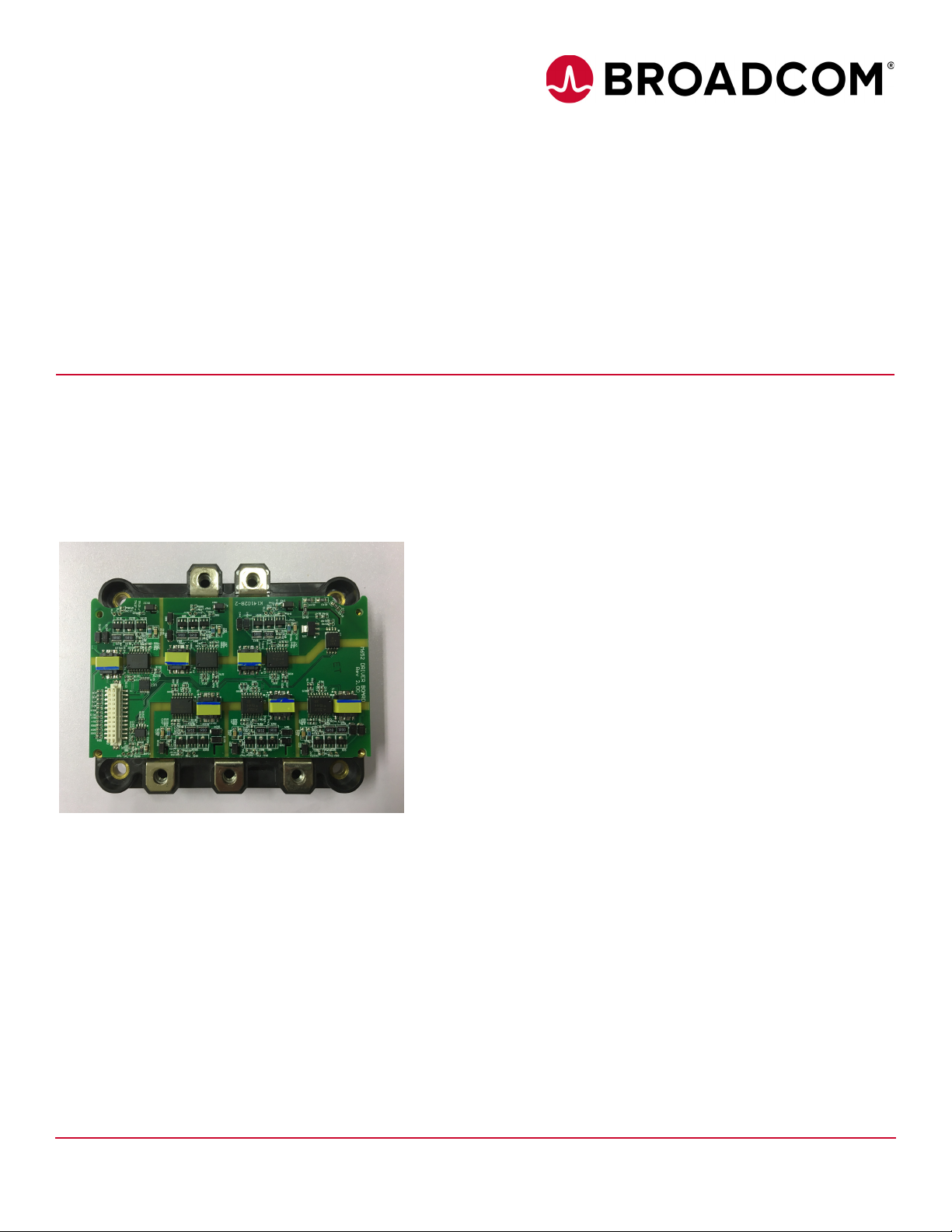
Evaluation Driver Board for Fuji M652 6-in-1 IGBT
User Guide
Introduction
This evaluation driver board is optimized for a Fuji M652 6-in-1
Integrated Gate Bipolar Transistor (IGBT ) module rated at 650V,
600A. It features 6 x ACPL-32JT for IGBT gate driving and 1 x
ACPL-C87AT for bus voltage sensing.
Figure 1 Evaluation Driver Board for Fuji M652 IGBT
An ACPL-32JT monitors each IGBT for short circuit events by
way of the collector voltage and triggers a local fault shutdown
sequence when required. A small gate discharge device slowly
reduces the short circuit collector current to prevent
overvoltage damage. The IGBT is shut off before the dissipated
energy can reach destructive levels.
Key Features
Gate Driver
The ACPL-32JT is an Automotive 2.5 Amp Gate Drive
Optocoupler. It features an integrated flyback controller for
isolated DC-DC converter, IGBT desaturation sensing, and
protection with soft-shutdown.
Integrated Flyback Controller
Each ACPL-32JT has an integrated DC-DC flyback controller
that is paired with a flyback transformer to provide a split rail
Vcc2 voltage of +15V/–5V with up to 2W of isolated power for
driving each IGBT. This distributed power supply architecture
removes the need for a separate monolithic power supply.
Bus Voltage Sensing
The ACPL-C87AT is an automotive unity-gain isolated voltage
sensor that utilizes superior optical coupling technology, with a
sigma-delta analog-to-digital converter, chopper stabilized
amplifiers, and a fully differential circuit topology to provide
unequaled isolation-mode noise rejection, low offset, high gain
accuracy, and stability.
An ACPL-C87AT is used with a resistor chain for bus voltage
sensing.
Fault Detection and Protection
The power stage of a typical three-phase inverter is susceptible
to destructive failures due to overcurrent and overvoltage
conditions.
Broadcom
- 1 -
Page 2
ACPL-32JT, ACPL-C87AT User Guide
Board Operation
Power Supply
The board accepts 8V to 18V applied across DC12 to GND1. The
nominal voltage is 12V.
PWM Inputs
There are six Pulse Width Modulation (PWM) inputs for driving
the IGBT module: PWMLW, PWMHW, PWMLV, PWMHV, PWMLU,
PWMHU.
0V: Input Low
5V: Input High (max 5.5V)
Signals are referenced to GND1.
The input LEDs of the ACPL-32JT gate drivers are driven by an
on-board current buffer.
Desat Fault Feedback
There are six Desat Fault feedback outputs, one for each IGBT:
FLU, FHU, FLV, FHV, FLW, FHW.
When fault on gate driver secondary side is detected, Fault
feedback is pulled Low.
Low: Desat Fault Detected
High (5V): No Fault
Board Design
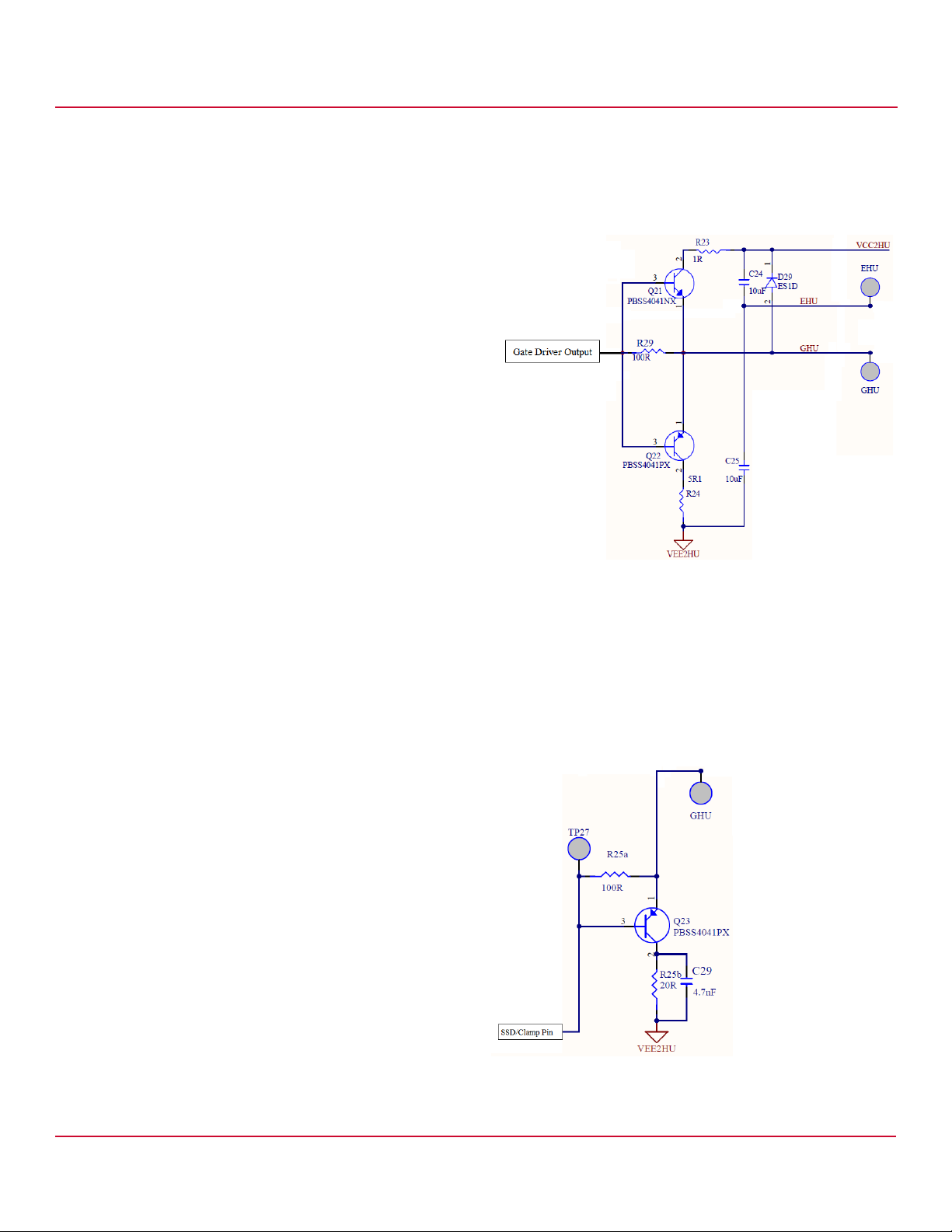
Gate Driving
Figure 2 Gate Driving
The Gate Driver output is connected to a push-pull buffer to
drive the IGBT gate.
The strength of the turn-on and turn-off is controlled by Ron
and Roff respectively (R23 and R24 in Figure 2).
UVLO Feedback
There are six Under-Voltage Lock Out (UVLO) feedback outputs,
one for each IGBT: ULU, UHU, ULV, UHV, ULW, UHW.
When undervoltage on gate driver secondary side is detected,
UVLO feedback is pulled Low.
Low: Undervoltage Detected
High (5V): Voltage Normal
Broadcom
Soft Shutdown
Figure 3 Soft Shutdown
- 2 -
Page 3
ACPL-32JT, ACPL-C87AT User Guide
The IGBT collector voltage is sensed by the ACPL-32JT gate
drivers through the Desat pin. When desaturation events are
detected, ACPL-32JT applies a soft shutdown to the IGBT gate
to prevent damage. A PNP buffer transistor is used to
customize the shutdown process. The shutdown strength is
controlled by Rssd and Cssd.
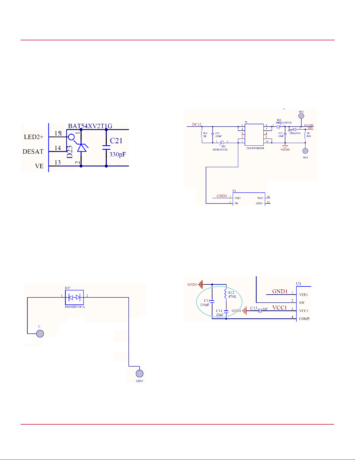
Desat Blanking
Figure 4 Desat Blanking
The total blanking time is calculated in terms of internal
blanking time tDESAT(BLANKING) (0.6 μs typ), external
capacitance CBLANK (330 pF), FAULT threshold voltage VDESAT
(7V typ), and DESAT charge current ICHG (0.9 mA typ) as
follows:
tBLANK = tDESAT(BLANKING) + (CBLANK × VDESAT/ICHG)
= 0.6 μs + (330 pF × 7V/0.9 mA)
~ 3.2 μs
Active Clamp
Figure 5 Active Clamp
A Transient Voltage Suppressor (TVS) rated at 510V is placed
between the Gate and Collector of the IGBT to provide active
clamp protection. Vce of the IGBT is clamped and protected by
the TVS.
DC/DC Converter
Figure 6 DC/DC Converter
Each ACPL-32JT Gate Driver integrates a DC/DC converter that
provides distributed power to the secondary side.
For DC12 = 8V to 18V, this circuit nominally supports a
secondary-side load of up to 60 mA (including Icc2 of
ACPL-32JT) at the regulated VCC2 voltage.
Figure 7 Compensation Network
The compensation network is referenced to a nominal
transformer of Lp = 60 μH, Ls = 260 μH.
Broadcom
- 3 -
Page 4

ACPL-32JT, ACPL-C87AT User Guide
Bus Voltage Sense Ratio
R146 R147+
R142 R143 R144 R145 R146 R147+++++
----------------------------------------------------------------------------------------------------------
=
2k 2k+
200k 200k 200k 200k 2k 2k+++++
-------------------------------------------------------------------------------------------
=
4.975 mV/V =
Bus Voltage Sensing
Bus voltage is sensed through a precision resistor chain. ACPL-C87AT optically isolates the signal for transmission to a
microcontroller (output Voltage Sense Output (VSO) on P1 header).
The Bus Voltage Sense Ratio may be calculated as follows:
Connection Interface (Connector Header P1)
Pin Name Typ e LEVEL Item Logic
1 FLU OUT TTL Fault Feedback for U-bottom L: Fault
3 ULU OUT TTL Under-Voltage Lock Out Feedback for
5 FLV OUT TTL Fault Feedback for V-bottom L: Fault
7 ULV OUT TTL Under-Voltage Lock Out Feedback for
9 FLW OUT TTL Fault Feedback for W-bottom L: Fault
11 ULW OUT TTL Under-Voltage Lock Out Feedback for
13 UHU OUT TTL Under-Voltage Lock Out Feedback for U-top L: Under-Voltage Lock Out
15 FHU OUT TTL Fault Feedback for U-top L: Fault
17 UHV OUT TTL Under-Voltage Lock Out Feedback for V-top L: Under-Voltage Lock Out
19 FHV OUT TTL Fault Feedback for V-top L: Fault
21 UHW OUT TTL Under-Voltage Lock Out Feedback for W-top L: Under-Voltage Lock Out
23 FHW OUT TTL Fault Feedback for W-top L: Fault
2 PWMLW IN TTL PWM input for W-bottom H: Led on, L: Led off
4 PWMHW IN TTL PWM input for W-top H: Led on, L: Led off
6 PWMLV IN TTL PWM input for V-bottom H: Led on, L: Led off
8 PWMHV IN TTL PWM input for V-top H: Led on, L: Led off
10 PWMLU IN TTL PWM input for U-bottom H: Led on, L: Led off
12 PWMHU IN TTL PWM input for U-top H: Led on, L: Led off
14 DC12 Power 8V to 18V DC power supply —
16 GND1 Ground Ground Low Voltage Side Ground —
18 GND1 Ground Ground Low Voltage Side Ground —
20 VSO OUT Analog
(0 to 2V)
22 OT1 OUT — Connection to IGBT NTC Thermistor Pin T1 —
24 OT2 OUT — Connection to IGBT NTC Thermistor Pin T2 —
U-bottom
V-bottom
W-bottom
Bus Voltage Sensor Output Analog (0 to 2V)
L: Under-Voltage Lock Out
L: Under-Voltage Lock Out
L: Under-Voltage Lock Out
Broadcom
- 4 -
Page 5
ACPL-32JT, ACPL-C87AT User Guide
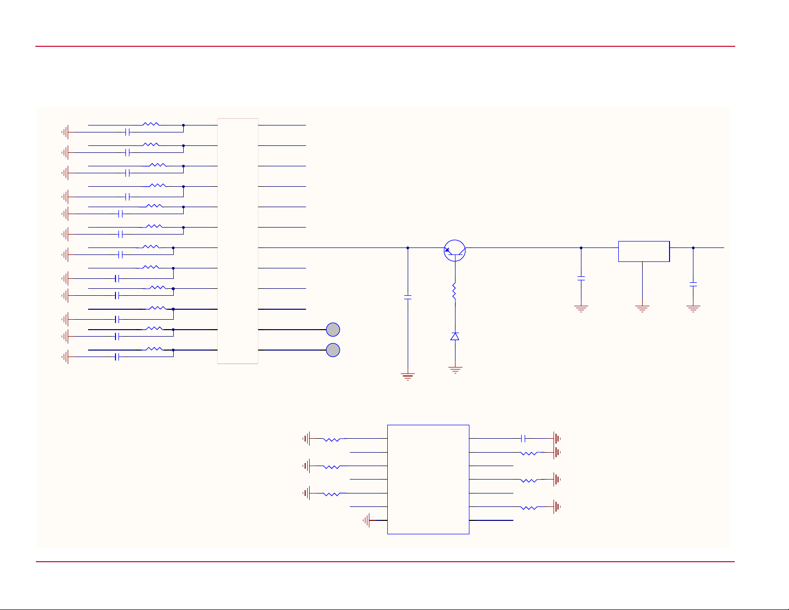
Circuit Schematic
M652 Driver Board
GND1
GND1
GND1
GND1
GND1
GND1
GND1
GND1
GND1
GND1
GND1
GND1
DC5
C36 1nF
DC5
C37 1nF
DC5
C76 1nF
DC5
C77 1nF
DC5
C116 1nF
DC5
C117 1nF
C16 1nF
DC5
C17 1nF
DC5
C56 1nF
DC5
C57 1nF
DC5
C96 1nF
DC5
C97 1nF
R34 4K7
R33 4K7
R74 4K7
R73 4K7
R114 4K7
R113 4K7
4K7
4K7
R14
R53 4K7
R54 4K7
R93 4K7
R94 4K7
P1
FLU
1 2
ULU
3 4
FLV
5 6
ULV
7 8
FLW
9 10
ULW
11 12
UHU
13
FHU
15
UHV
17
FHV
19
UHW OT1
21
FHW OT2
23
DF11CZ24DS2V22
PWMLW
PWMHW
PWMLV
14
16
18
20
22
24
PWMHV
PWMLU
PWMHU
DC12
GND1
GND1
VSO
GND1
C11
10uF
1
GND1
Q161
2
FCX591A
3
R161
1K
1
D66
MMSZ4689ET1G
2
U11
NCV8664ST50T3G
0.1uF
1
VIN
OUT
GND
2
GND1GND1
VCC1DC12DC5 R13
C131
DC5
3
C132
10uF
GND1
GND1
GND1
GND1
R162
5K
R163
5K
R164
5K
PWMHU
PWMALU
PWMHV
PWMAHV
GND1
1
2
3
4
5
6
7
Broadcom
- 5 -
U12
1A
1Y
2A
2Y
3A
3Y
GND
SN74AC04-Q1
VCC
DC5
14
PWMLVPWMAHU
13
6A
PWMALVPWMLU
12
6Y
11
PWMLW
5A
10
PWMALW
5Y
9
PWMHW
4A
8
PWMAHW
4Y
C161
0.1uF
5K
R165
R166 5K
R167 5K
GND1
GND1
GND1
GND1
Page 6

ACPL-32JT, ACPL-C87AT User Guide
R22a
51R
1K
R21
12
D22
MURA160T3G
GND1
1uF
C15
330pF
C21
1uF
C23a
VEE2HU
12
D23
BAT54XV2T1G
C
EHU
GHU
VEE1
1
SW
2
VCC1
3
COMP
4
/UVLO
5
/FAULT
6
AN
7
CA
8
VEE2
9
SSD/CLAMP
10
VO
11
VCC2
12
VE
13
DESAT
14
LED2+
15
VEE2
16
U1
ACPL-32JT
VCC1
GND1
R12
470K
C14
22nF
C13
330pF
GND1
PWMAHU
R15 5K1
VCC2HU
VEE2HU
R23
1R
R24
5R1
10uF
C24
1
3
2
Q21
PBSS4041NX
1
3
2
Q22
PBSS4041PX
R25a
100R
VCC2HU
GHU
VEE2HU
UHU
FHU
C25
10uF
EHU
C
R16
110R
R17
110R
12
D29
ES1D
TP21
TP27
1 2
D27
P6SMB510CA
1
3
2
Q23
PBSS4041PX
VEE2HU
R27
NM
C26
33nF
NM
R28c
R29
100R
0R
R28a
R25b
20R
TP22
1uF
C23b
DC5
C27
NM
C28
NM
C29
4.7nF
1
12
D21
MBRS1100T3G
1 2
D11
MURS105T3G
R112KC12
220nF
1
2
3
4
5 6
7
8
9
10
T1
TRANSFORMER
VCC2HU
DC12
VEE2HU
1 2
D24
1SMA4744
R26
1K
EHU
C22
10uF
TP24
TP23
TP26
TP25
M652 Driver Board: U-Top
Broadcom
- 6 -
Page 7

ACPL-32JT, ACPL-C87AT User Guide
ELU
GLU
GND1
1uF
C35
330pF
C41
1uF
C43
51R
R42a
VEE2LU
1K
R41
1
2
BAT54XV2T1G
D43
EHU
VEE1
1
SW
2
VCC1
3
COMP
4
/UVLO
5
/FAULT
6
AN
7
CA
8
VEE2
9
SSD/CLAMP
10
VO
11
VCC2
12
VE
13
DESAT
14
LED2+
15
VEE2
16
U2
ACPL-32JT
VCC1
GND1
R32
470K
C34
22nF
C33
330pF
GND1
12
D41
MBRS1100T3G
1 2
D31
MURS105T3G
R312KC32
220nF
1
2
3
4
5 6
7
8
9
10
T2
TRANSFORMER
VCC2LU
DC12
PWMALU
R35 5K1
VCC2LU
VEE2LU
1R
R43
5R1
R44
10uF
C44
1
3
2
Q41
PBSS4041NX
1
3
2
Q42
PBSS4041PX
R45a
100R
VCC2LU
GLU
VEE2LU
ULU
FLU
C45
10uF
R47
NM
33nF
C46
R36
110R
R37 110R
1 2
D44
1SMA4744
R46
220R
ELU
C42
10uF
VEE2LU
12
D42
MURA160T3G
12
D49
ES1D
TP41
TP43
TP47
TP44
1 2
D47
P6SMB510CA
1
3
2
Q43
PBSS4041PX
VEE2LU
NM
R48a
100R
R49
0R
R48b
TP42
DC5
1uF
C43b
R45b
20R
C49
4.7nF
C48
NM
C47
NM
TP46
TP45
M652 Driver Board: U-Bottom
Broadcom
- 7 -
Page 8

ACPL-32JT, ACPL-C87AT User Guide
EHV
GHV
GND1
1uF
C55
330pF
C61
1uF
C63a
R62a
51R
VEE2HV
1K
R61
12
BAT54XV2T1G
D63
C
VEE1
1
SW
2
VCC1
3
COMP
4
/UVLO
5
/FAULT
6
AN
7
CA
8
VEE2
9
SSD/CLAMP
10
VO
11
VCC2
12
VE
13
DESAT
14
LED2+
15
VEE2
16
U3
ACPL-32JT
VCC1
GND1
R52
470K
C54
22nF
C53
330pF
GND1
12
D61
MBRS1100T3G
1 2
D51
MURS105T3G
R512KC52
220nF
1
2
3
4
5 6
7
8
9
10
T3
TRANSFORMER
VCC2HV
DC12
VEE2HV
PWMAHV
R55 5K1
VCC2HV
VEE2HV
1R
R63
5R1
R64
10uF
C64
1
3
2
Q61
PBSS4041NX
1
3
2
Q62
PBSS4041PX
R65a
100R
VCC2HV
GHV
UHV
FHV
C65
10uF
VEE2HV
R67
NM
33nF
C66
R56
110R
R57
110R
1 2
D64
1SMA4744
R66
1K
EHV
C62
10uF
12
D62
MURA160T3G
1
2
D69
ES1D
TP61
TP67
TP63
TP64
1 2
D67
P6SMB510CA
1
3
2
Q63
PBSS4041PX
VEE2HV
0R
R68b
NM
R68a
100R
R69
TP62
DC5
1uF
C63b
R65b
20R
C69
4.7nF
C67
NM
C68
NM
TP66
TP65
M652 Driver Board: V-Top
Broadcom
- 8 -
Page 9

ACPL-32JT, ACPL-C87AT User Guide
ELV
GLV
GND1
1uF
C75
330pF
C81
1uF
C83a
R82a
51R
VEE2LV
1K
R81
12
BAT54XV2T1G
D83
EHV
VEE1
1
SW
2
VCC1
3
COMP
4
/UVLO
5
/FAULT
6
AN
7
CA
8
VEE2
9
SSD/CLAMP
10
VO
11
VCC2
12
VE
13
DESAT
14
LED2+
15
VEE2
16
U4
ACPL-32JT
VCC1
GND1
R72
470K
C74
22nF
C73
330pF
GND1
12
D81
MBRS1100T3G
1 2
D71
MURS105T3G
R712KC72
220nF
1
2
3
4
5 6
7
8
9
10
T4
TRANSFORMER
VCC2LV
DC12
VEE2LV
PWMALV
R75 5K1
VCC2LV
VEE2LV
1R
R83
5R1
R84
10uF
C84
1
3
2
Q81
PBSS4041NX
1
3
2
Q82
PBSS4041PX
R85a
100R
VCC2LV
GLV
VEE2LV
ULV
FLV
C85
10uF
R87
NM
33nF
C86
R76
110R
R77
110R
1 2
D84
1SMA4744
R86
1K
ELV
C82
10uF
12
D82
MURA160T3G
1
2
D89
ES1D
TP81
TP83
TP87
TP84
1 2
D87
P6SMB510CA
1
3
2
Q83
PBSS4041PX
VEE2LV
0R
R88b
NM
R88a
100R
R89
TP82
DC5
1uF
C83b
R85b
20R
C89
4.7nF
C88
NM
C87
NM
TP86
TP85
M652 Driver Board: V-Bottom
Broadcom
- 9 -
Page 10

ACPL-32JT, ACPL-C87AT User Guide
EHW
GHW
GND1
1uF
C95
330pF
C101
1uF
C103a R102a
51R
VEE2HW
1K
R101
12
BAT54XV2T1G
D103
C
VEE1
1
SW
2
VCC1
3
COMP
4
/UVLO
5
/FAULT
6
AN
7
CA
8
VEE2
9
SSD/CLAMP
10
VO
11
VCC2
12
VE
13
DESAT
14
LED2+
15
VEE2
16
U5
ACPL-32JT
VCC1
GND1
R92
470K
C94
22nF
C93
330pF
1
12
D101
MBRS1100T3G
1 2
D91
MURS105T3G
R91
2K
C92
220nF
1
2
3
4
5 6
7
8
9
10
T5
TRANSFORMER
VCC2HW
DC12
VEE2HW
PWMAHW
R95 5K1
VCC2HW
VEE2HW
1R
R103
5R1
R104
10uF
C104
1
3
2
Q101
PBSS4041NX
1
3
2
Q102
PBSS4041PX
R105a
100R
VCC2HW
GHW
VEE2HW
UHW
FHW
C105
10uF
R10
NM33nF
C106
R96
110R
R97
110R
1 2
D104
1SMA4744
R106
1K
EHW
C102
10uF
12
D102
MURA160T3G
12
D109
ES1D
TP101
TP103
TP107
TP104
1 2
D107
P6SMB510CA
1
3
2
Q103
PBSS4041PX
VEE2HW
0R
R108b
NM
R108a
100R
R109
TP102
DC5
1uF
C103b
R105b
20R
C109
4.7nF
C108
NM
C107
NM
TP106
TP105
M652 Driver Board: W-Top
Broadcom
- 10 -
7
GND
Page 11

ACPL-32JT, ACPL-C87AT User Guide
ELW
GLW
GND1
1uF
C115
330pF
C122
1uF
C123a
R122a
51R
VEE2LW
1K
R121
12
BAT54XV2T1G
D123
EHW
VEE1
1
SW
2
VCC1
3
COMP
4
/UVLO
5
/FAULT
6
AN
7
CA
8
VEE2
9
SSD/CLAMP
10
VO
11
VCC2
12
VE
13
DESAT
14
LED2+
15
VEE2
16
U6
ACPL-32JT
VCC1
GND1
R112
470K
C114
22nF
C113
330pF
GND
1
12
D121
MBRS1100T3G
1 2
D111
MURS105T3G
R1112KC112
220nF
1
2
3
4
5 6
7
8
9
10
T6
TRANSFORMER
VCC2LW
DC12
VEE2LW
PWMALW
R115 5K1
VCC2LW
VEE2LW
1R
R123
5R1
R124
10uF
C124
1
3
2
Q121
PBSS4041NX
1
3
2
Q122
PBSS4041PX
R125a
100R
VCC2LW
GLW
VEE2LW
ULW
FLW
C125
10uF
R127
NM
33nF
C126
R116
110R
R117
110R
1 2
D124
1SMA4744
R126
1K
ELW
C121
10uF
12
D122
MURA160T3G
1
2
D129
ES1D
TP121
TP123
TP127
TP124
1 2
D127
P6SMB510CA
1
3
2
Q123
PBSS4041PX
VEE2LW
0R
R128b
NM
R128a
100R
R129
TP122
DC5
1uF
C123b
R125b
20R
C129
4.7nF
C127
NM
C128
NM
TP126
TP125
M652 Driver Board: W-Bottom
Broadcom
- 11 -
Page 12

VDD1
1
VIN+
2
SD
3
GND14GND2
5
VOUT-
6
VOUT+
7
VDD2
8
VDD
N
T
U7
ACPL-C87AT
20K
R152
20K
R153
20KR155
20KR154
1uF
C143
R146
2K 0.1%
R145
200K 0.1%
1
V-
4
3
2
5
6
7
V+
8
U31
OPA2171AIDR
R144
200K 0.1%
R143
200K 0.1%
R142
200K 0.1%
R147
2K 0.1%
1uF
C151
2K
R157
10K
R156
0.1uF
C155
1nF
C152
0.1uF
C154
39R
R148
10nF
C144
1nFC153
ELU
C
C142
10uF
VCC2LU
GND1
GND1
GND1
GND1
GND1 GND1
VSO
10R
R141
10R
R151
DC5
GND
2
OUT
3
VIN
1
U21
NCV8664ST50T3G
C141
0.1uF
ELU
R158
0R
GND1
NM
R159
ELU ELU
ELU
ELU
10R
R168
DC5
ACPL-32JT, ACPL-C87AT User Guide
M652 Driver Board: Bus Voltage Sensing
ND
U
ND
Broadcom
- 12 -
Page 13

ACPL-32JT, ACPL-C87AT User Guide
Board Dimensions
Broadcom
- 13 -
Page 14

ACPL-32JT, ACPL-C87AT User Guide
Component Location — Top
Broadcom
- 14 -
Page 15

ACPL-32JT, ACPL-C87AT User Guide
Component Location — Bottom
Broadcom
- 15 -
Page 16

For product information and a complete list of distributors, please go to our web
site: www.broadcom.com.
Broadcom, the pulse logo, Connecting everything, Avago Technologies, Avago,
and the A logo are among the trademarks of Broadcom in the United States,
certain other countries and/or the EU.
Copyright © 2017 Broadcom. All Rights Reserved.
The term "Broadcom" refers to Broadcom Limited and/or its subsidiaries. For
more information, please visit www.broadcom.com.
Broadcom reserves the right to make changes without further notice to any
products or data herein to improve reliability, function, or design.
Information furnished by Broadcom is believed to be accurate and reliable.
However, Broadcom does not assume any liability arising out of the application
or use of this information, nor the application or use of any product or circuit
described herein, neither does it convey any license under its patent rights nor
the rights of others.
January 24, 2017 – ACPL-32JT-C87AT-UG100
 Loading...