

Page 1

TABLE OF CONTENTS
PARAGRAPH PAGE NO.
SECTION I POWER SUPPLY THEORY OF OPERATION
1-1 Introduction 1-1
1-3 General Description 1-1
1-6 AC Input 1-1
1-8 Conventional Rectifier Circuitry 1-1
1-10 Soft-Start Circuit 1-1
1-12 AC Line Detection/Synchronization 1-2
1-15 Soft-Start Control Circuit 1-2
1-18 Power Factor Corrector Circuit Board Control Circuit 1-2
1-20 SCR Controlled Rectifier Circuit 1-5
1-23 Filter Circuit 1-5
1-25 Power Supply Enable Circuit 1-5
1-28 Switching Regulator Circuit 1-5
1-30 Low Voltage Power Supply 1-6
1-31 Switching Regulator Control Circuit 1-6
1-33 Switching Regulator Circuit Operation 1-6
1-34 Power Control/Correction Circuit 1-6
1-38 Fault Detection 1-7
1-43 Crowbar Circuit 1-7
1-47 Power Supply Circuit Grounds 1-8
SECTION II POWER SUPPLY CIRCUIT BOARD MAINTENANCE
2-1 Introduction 2-1
2-3 Safety Considerations 2-1
2-6 First Level Maintenance 2-1
2-8 Cleaning and Inspection 2-1
2-10 Second Level Maintenance 2-2
2-12 Troubleshooting 2-2
2-13 Safety Considerations 2-2
2-14 Removing/Installing a Power Supply Circuit Board 2-2
2-17 Troubleshooting Procedures 2-3
2-18 Component Replacement Procedure 2-4
SECTION III POWER SUPPLY CIRCUIT BOARD PARTS LIST
3-1 Introduction 3-1
SECTION IV POWER SUPPLY CIRCUIT BOARD DRAWINGS
4-1 Introduction 4-1
LIST OF ILLUSTRATIONS
FIGURE TITLE PAGE NO.
1-1 POWER SUPPLY CIRCUIT BOARD 1-3
SIMPLIFIED SCHEMATIC
LIST OF TABLES
TABLE TITLE PAGE NO.
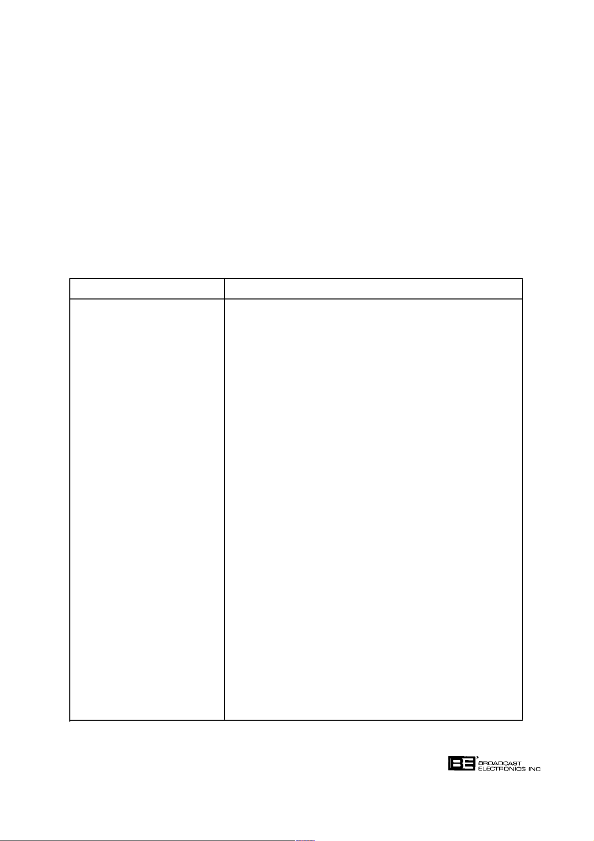
2-1 POWER SUPPLY MODULE TROUBLESHOOTING 2-3
3-1 REPLACEABLE PARTS LIST INDEX 3-1
Page 2

SECTION I
POWER SUPPLY THEORY OF OPERATION
1-1. INTRODUCTION.
1-2. This section presents a general description of the Broadcast Electronics AM-10A/AM-6A
transmitter power supply assembly.
1-3.
1-4. DC operating potentials for the RF power modules are provided by power supply assemĆ
1-5. The modular design of the power supply assembly allows the power supply circuit board
1-6.
1-7. AC power from the ac input switch is applied through fuses F6 and F7 to power trans-
1-8.
1-9. AC power from a winding of power transformer T1 is applied to bridge rectifier D11. D11
GENERAL DESCRIPTION.
blies (refer to Figure 1-1). The power supply assembly consists of: 1) a power supply cirĆ
cuit board and 2) filter and transformer components located on a power supply panel.
One power supply assembly provides dc operating potentials for one power block. The
AM-10A transmitter is equipped with 5 power supply assemblies. The AM-6A transmitter is equipped with 3 power supply assemblies.
to be removed from the transmitter for maintenance. The following text presents a deĆ
scription of the power supply circuit board and the components located on the power supply panel assembly.
AC INPUT.
former T1. Fuses F6 and F7 protect the circuitry from over-current conditions. TransĆ
former T1 consists of: 1) a single primary winding and 2) five secondary windings. The
transformer is designed to provide low-voltage ac samples for application to five convenĆ
tional bridge rectifier circuits.
CONVENTIONAL RECTIFIER CIRCUITRY.
rectifies the ac potential into an unregulated 30V dc supply for application to the RF power
module power amplifier circuit boards. Capacitor C21 provides filtering for the supply. AC
power from a second winding of transformer T1 is applied to bridge rectifier D10. D10 recĆ
tifies the ac potential into an unregulated +20V dc supply for the power supply circuit
board circuitry. Capacitor C20 provides filtering for the supply. AC power from a third
winding of ac power transformer T1 is applied to bridge rectifier D9. D9 rectifies the ac
potential into an unregulated +20 volt dc supply for application to: 1) the modulator circuit board and 2) to regulator U3. U3 is a +15 volt dc regulator. The output of U3 routed
for application to the components on the power supply circuit board. AC power from a
fourth winding of power transformer T1 is applied to bridge rectifier D12. D12 rectifies
the ac potential into an unregulated +15V dc supply for application to: 1) the power supply circuit board and 2) regulator U4. U4 is a +12 volt dc regulator. The output of U4
routed for application to the components on the power supply circuit board. An ac sample
from the winding is routed for application to a soft-start circuit. Capacitor C15 provides
filtering for the supply.
1-10.
1-11. An ac sample from the winding of T1 is also routed to a soft-start circuit. The soft-start
SOFT-START CIRCUIT.
circuit is designed to eliminate component stress during turn-on by limiting the current
in-rush. The circuit consists of an ac line detection/synchronization and soft-start control
circuits.
1-1
Page 3

1-12. AC LINE DETECTION/SYNCHRONIZATION. An ac sample from a winding of transformĆ
er T1 is rectified by diodes D7 and D8 and applied to integrated circuit U6B. U6B funcĆ
tions as a zero phase detector. As the ac line phase approaches zero degrees, U6B will
output a HIGH pulse. The HIGH pulse is applied to: 1) transistor Q2, 2) transistor Q7 of
the soft-start circuit, and 3) ac line detector U5A/U5B. The pulse biases transistor Q2
and optical coupler U2 on. Q2 and U2 will output a pulse each time the ac line phase is
zero. As a result, U2 will output a 120 Hz signal to the controller circuit board.
1-13. U5A and U5B function as an ac line voltage detector. When ac line voltage is present,
U5A will output a LOW. The LOW allows transistor Q3 to be biased on. With Q3 on, a
+12 volt dc signal is applied to optical coupler U1. When a power supply enable and a
PWM OK signal is applied to U1, U1 will output a reference voltage to a soft-start control
circuit for power supply operation. When ac line voltage is not present, U5A will output a
HIGH, the HIGH biases transistor Q3 off to terminate power supply operation. When ac
power is re-applied, U5B will maintain a HIGH for 100 milliseconds to allow the circuit to
stabilize during turn-on operations.
1-14. In addition to the ac line voltage detection circuit, integrated circuit U6A functions as a
low line voltage detector. When the dc supply is above the threshold at U6A, U6A will
output a LOW to bias transistor Q1 off. As a result, a HIGH ac OK signal indicating acĆ
ceptable ac line voltage is applied to optical coupler U9. When the dc supply is below 185
volts, U6A will output a HIGH to bias transistor Q1 on. As a result, a LOW ac OK signal
indicating low ac line voltage is applied to optical coupler U9. When the voltage increases
to approximately 190 volts, the output of U6A will go LOW to enable the power supply.
1-15. This circuit is also used to detect high ac line voltage potentials. If the ac line voltage is
above approximately 270 volts, transistor Q28 will be biased on. With Q28 on, the input
to U6A will be muted. When the input is muted: 1) the transmitter output power will be
muted and 2) no transmitter fault or emergency condition will be generated.
1-16.
1-17. The circuit generates the soft-start pulses from two signals: 1) a ramp signal and 2) a
1-18.
1-19. Transistors Q26 and Q27 control a power factor corrector circuit board (not used in
SOFT-START CONTROL CIRCUIT. The soft-start control circuit consists of: 1) transistors
Q4 through Q9 and 2) integrated circuit U7. The circuit is designed to generate short
duration pulses in each time the ac line waveform crosses the 0 volt axis. The pulses are
applied to an SCR controlled rectifier to slowly bias the components on during initial start
operations. This operation eliminates the component stress at power-on by limiting the
supply in-rush current.
triangle signal. The ramp signal is generated by transistors Q4 and Q5. When ac line
voltage is detected, a +12 volt signal from U1 is applied to transistor Q4. Q4 operates in
association with capacitor C16 and transistor Q5 to generate a ramp voltage. The
triangle signal is generated by transistors Q6 and Q7. Pulses from U6B are applied to
transistor Q7. Q7 operates in association with capacitor C17 and transistor Q6 to generate a triangle signal. The triangle signal and the ramp signal are applied to comparator
U7. U7 responds by generating a square-wave signal with a short duty cycle when the ac
line phase is zero. The square-wave signal from U7 is applied to soft-start driver transisĆ
tors Q8 and Q9. Q8 and Q9 will slowly bias the rectifier circuit on to limit the current
in-rush.
POWER FACTOR CORRECTOR CIRCUIT BOARD CONTROL CIRCUIT.
A-Series AM transmitters). During soft-start operation, ramp voltage will drop below
approximately 3V. When this occurs, the output of transistor Q26 will go LOW. This
LOW biases transistor Q27 on. With Q27 on, a LOW energizes two relays on the power
factor corrector circuit board. With the relays energized, a capacitor is inserted into the
circuit to enable power factor correction.
1-2
Page 4
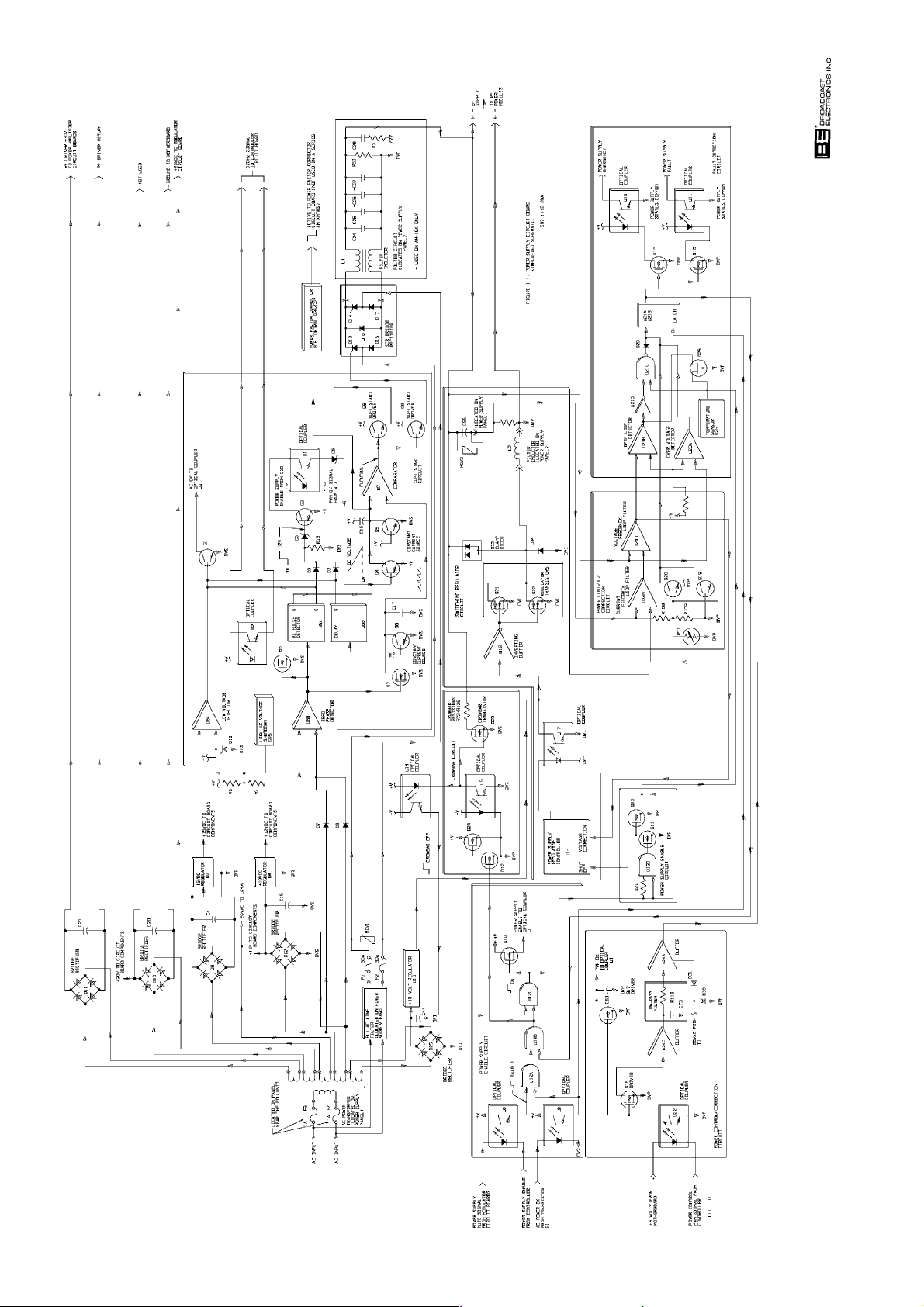
597-1112-28A
COPYRIGHT © 1997 BROADCAST ELECTRONICS, INC
(1-3/1-4)
SIMPLIFIED SCHEMATIC
FIGURE 1-1. POWER SUPPLY CIRCUIT BOARD
Page 5

1-20. SCR CONTROLLED RECTIFIER CIRCUIT.
1-21. The ac line voltage is rectified into a main dc supply for the modulator and amplifier cirĆ
cuitry by an SCR controlled bridge rectifier circuit. Primary ac power for the main dc
supply is applied to ac line filter FL1. FL1 is a modular line filter designed to protect the
circuitry from EMI. The ac from filter FL1 is applied to fuses F1 and F2. The fuses protect the power supply circuitry from over-current conditions. Metal-Oxide-Varistor
MOV1 prevents damage to the rectifier circuitry from ac line voltage surge potentials.
1-22. The SCR controlled rectifier circuit consists of diodes D15 through D17 and SCRs D13
and D14. The rectifier circuit is controlled by the soft-start control circuit. When power
is required from the circuit, the soft-start circuit will output synchronized ac line pulses
to SCRs D13 and D14. The SCRs will respond by slowly biasing the rectifier circuit on.
The rectifier will output an unregulated and unfiltered dc supply at a maximum of 300V
to an inductor and capacitor filter network located on the power supply panel.
1-23.
1-24. The output of the rectifier circuit is applied to a filter network consisting of inductor L1
1-25.
1-26. The power supply is controlled by a: 1) power supply enable signal from the controller
1-27. When a power supply mute operation is required, an RF power module modulator circuit
FILTER CIRCUIT.
and capacitors C24 through C27. The filter is designed to remove the ripple in the supply.
The output of the capacitor network generates the positive leg of the B supply. The B supĆ
ply is the main operating supply for the RF power modules. The negative leg of the B
supply is generated by a switching regulator circuit (refer to the following text).
POWER SUPPLY ENABLE CIRCUIT.
and 2) power supply mute signal from the modulator circuit boards. When power supply
operation is required, the controller will output a LOW power supply enable signal to optiĆ
cal coupler U8. With no mute signals present, U8 will output a HIGH to AND gate U12A.
With a HIGH ac OK signal from U9 indicating the presence of ac power and no power
supply faults, U12A will output a HIGH to U12B. With a HIGH from U21A/U21B, U12B
will output a HIGH to U12C and to Q12. With a HIGH from U14 indicating the crowbar
circuit is off, U12C will output a HIGH after a one second delay to: 1) transistor Q10,
2) AND gate U12D, and 3) NAND gate U21C. The HIGH biases Q12 and U15 on to disable the crowbar circuit. Q10 will respond by routing a HIGH power supply enable signal
to optical coupler U1. U1 will output a dc voltage to enable the power supply soft-start
circuit. AND gate U12D will output a HIGH to transistor Q11. The HIGH biases Q11 on
to enable regulator controller U13 and bias Q13 off.
board will output a mute signal to optical coupler U8. U8 will output a LOW to AND gate
U12A. With a HIGH ac OK signal from U9, U12A will output a LOW to U12B. U12B will
output a LOW to U12C and to Q12. The LOW biases Q12 and U15 off to enable the crowĆ
bar circuit. U12C will output a LOW to: 1) transistor Q10, 2) AND gate U12D. Q10 will
be biased off to terminate power supply operation by disabling the drive to the SCR rectifiĆ
er circuit. U12D will disable Q11 which allows a HIGH to disable regulator controller
U13 and bias Q13 on. Q13 will output a LOW to disable the fault detection circuit to preĆ
vent erroneous fault indications during mute conditions.
1-28.
1-29. The B supply is regulated and controlled by a switching regulator circuit. The switching
SWITCHING REGULATOR CIRCUIT.
regulator circuit generates the - leg of the B supply and consists of: 1) a low voltage power supply circuit, 2) a power control network, 3) optical coupler U17, 4) inverting buffer
U19, and 5) switching regulator transistors Q21 and Q22.
1-5
Page 6

1-30. LOW VOLTAGE POWER SUPPLY. A dc operating supply for the optical couplers and the
inverting buffers is generated by bridge rectifier D25. D25 full-wave rectifies an ac potential from ac transformer T1 into an unregulated +20V supply. The supply is applied to
+18V regulator U16. The output of U16 is further regulated to a 5V operating potential
by a resistive divider and a zener diode. The 5V supply is applied to optical coupler U17
and buffer U19.
1-31.
1-32. Integrated circuit U13 functions as the switching regulator controller. U13 is a PWM outĆ
1-33.
1-34.
SWITCHING REGULATOR CONTROL CIRCUIT. The switching regulator circuit is conĆ
trolled by: 1) regulator controller U13 and 2) a power control/correction circuit. The cirĆ
cuits function in a closed-loop to control the operation of the switching regulator. As a
result, the regulator outputs a precision dc operating voltage at the appropriate level for
application to the RF power modules.
put device designed to produce two out-of-phase square wave signals with varying duty
cycles. The duty cycle is varied in response to the signal from the voltage correction cirĆ
cuit. With a correction voltage present at U13, U13 will output a PWM square wave signal to optical coupler U17. U17 provides isolation for the transition of the signal from two
different circuit ground potentials. The output of coupler U17 is inverted by inverting
buffer U19.
SWITCHING REGULATOR CIRCUIT OPERATION. The PWM output of U19 is applied to
the gates of IGBT (insulated-gate-bipolar-transistor) switching regulator transistors Q21
and Q22. The transistors function to regulate the negative leg of the B supply. The out-
put of the transistor switching regulator circuit is applied to filter inductor L2. Protection
of the transistors from switching transients during turn on/off operation is provided by
clamp diode D32. Capacitor C55 provides filtering for the negative leg of the B supply.
The output of the regulator circuit (B- leg) is applied to circuitry on the modulator circuit
board.
POWER CONTROL/CORRECTION CIRCUIT.
1-35. The switching regulator output voltage is controlled by a PWM (pulse-width-modulated)
signal from the controller. The PWM signal is a 1 kHz square-wave signal with a duty
cycle which varies in response to different power levels. The PWM signal from the controller is applied to optical coupler U22. With a +5 volt signal from the motherboard, U22
will output the PWM signal to transistors Q17 and Q18. Q17 will discharge capacitor C63
when a 1 kHz control signal is present. C63 will output a LOW PWM OK signal to optical
coupler U1. Q18 inverts the power control PWM signal. The output of Q18 is applied
through buffer U24C to a low-pass filter consisting of: 1) resistors R115, R116, and R117
and 2) capacitors C75, C76, and C77. The filter converts the power control PWM squarewave signal into a dc control voltage. The voltage is routed through buffer U24A to U24B.
1-36. U24B functions as a current feedback loop filter. U24B differentially amplifies the dc conĆ
trol voltage and a current sample from the switching regulator output filter capacitor. As
a result, U24B produces a dc control voltage for application to U24D.
1-37. U24D functions as a voltage feedback loop filter. U24D differentially amplifies the control
voltage from U24B and a voltage sample from the B+ leg of the supply. As a result,
U24D produces a dc control voltage for application to: 1) switching regulator controller
U13 and 2) a fault detection circuit. U13 will respond to the correction voltage by changing the duty cycle of the PWM drive signal to optical coupler U17. The switching regulator circuit will respond by changing the output voltage to a level required by the power
control PWM signal.
1-6
Page 7

1-38. FAULT DETECTION.
1-39. A fault detection circuit monitors the regulator for four conditions: 1) over-voltage,
2) open-loop, 3) over-current, and 4) over temperature. Over-voltage conditions are
monitored by U23A. U23A compares a sample of the B+ leg to a reference voltage. When
the B+ sample exceeds the reference voltage, the output of U23A will go LOW. The LOW
is routed to fault detector latch U21A/U21B. Open-loop conditions are monitored by
U23B. U23B compares a correction voltage sample to a reference voltage. When the
correction voltage sample exceeds the reference, the output of U23B will go LOW. The
LOW is inverted at U21D and applied to NAND gate U21C. With a HIGH power supply
enable signal from U12C, U21C will output a LOW to fault detector latch U21A/U21B.
1-40. Over-current conditions are monitored by transistors Q19 and Q20. When an over-curĆ
rent condition occurs, Q19 and Q20 will output a LOW. The LOW is routed to fault detecĆ
tor latch U21A/U21B. Over-temperature conditions are monitored by temperature sensor
U25. When the power supply temperature exceeds 72 degrees C, U25 will output a LOW
through transistor Q25 to U21D. The LOW is inverted at U21D and applied to NAND
gate U21C.
1-41. With a LOW from U21C or U23A, latch U21A/U21B will: 1) output a HIGH to transistor
Q16 and 2) output a LOW to transistor Q15 and to U12B. Transistor Q16 will be biased
on and will output a LOW to enable optical coupler U11. U11 will respond by generating
a power supply fault signal. AND gate U12B will output a LOW to: 1) disable regulator
controller U13, 2) disable the SCR controlled rectifier circuit, and 3) initiate a logic seĆ
quence to enable the crowbar circuit (refer to the following text). Transistor Q15 will be
biased off and will disable optical coupler U10. The output of U10 will open.
1-42. The output of U10 is connected in parallel with U10 on each power supply circuit board.
When the output of U10 on each power supply circuit board is open, a HIGH power supply emergency signal to be applied to the controller. The power supply emergency signal
indicates all power supply modules contain fault conditions.
1-43.
1-44. The power supply circuit board is equipped with a crowbar circuit to discharge the B supĆ
1-45. During a power supply off, ac off, or power supply mute condition, AND gate U12A will
1-46. When U15 is biased off, optical coupler U14 will also be disabled. With U14 disabled, a
CROWBAR CIRCUIT.
ply during power supply off, ac off, and power supply mute conditions. The crowbar circuit consists of: 1) crowbar MOSFET Q23 and 2) resistor R72. Control of the circuit is
provided by logic gates which monitor power supply off, ac off, and power supply mute
conditions.
output a LOW to U12B. With a HIGH from U21A/U21B, U12B will output a LOW to
transistor Q12. The LOW biases Q12 and optical coupler U15 off. As a result, a HIGH is
applied to the gate of crowbar MOSFET Q23. The HIGH biases Q23 on to short the B
supply and discharge capacitors C24, C25, C26, C27 and C55. Resistor R72 limits the curĆ
rent during shorting operations.
LOW is applied to U12C. U12C will output a LOW to disable the PWM drive to the
switching regulator circuit.
1-7
Page 8

1-47. POWER SUPPLY CIRCUIT GROUNDS.
1-48. The power supply circuit board is equipped with three isolated circuit grounds: 1) 0VS,
2) 0VP, and 3) 0VI. The circuit grounds are at different potentials and are not referenced
to earth ground. The 0VS ground is the circuit ground for the: 1) SCR controlled bridge
rectifier circuit, 2) soft-start control circuit, 3) ac line voltage detector circuit, and 4) lowvoltage detection circuit. The 0VP circuit ground is used to create the negative leg of the
B supply. The 0VI ground is the circuit ground for the: 1) crowbar circuit, 2) switching
regulator circuit, 3) inverting drive buffers, and 4) switching regulator transistors. The
circuit grounds are used in association with the circuitry to generate the operating voltages for the RF power modules.
1-8
Page 9
SECTION II
POWER SUPPLY CIRCUIT BOARD MAINTENANCE
2-1. INTRODUCTION.
2-2. This section provides maintenance information for the AM-10A/AM-6A transmitter
power supply circuit board assembly.
2-3.
SAFETY CONSIDERATIONS.
WARNING
THE TRANSMITTER CONTAINS MULTIPLE CIRCUIT
GROUNDS WITH HIGH AC AND DC POTENTIALS
WARNING
WARNING
WARNING
WITH RESPECT TO THE CABINET WHICH IS AT
EARTH POTENTIAL. DO NOT ENERGIZE THE
TRANSMITTER WITH TEST EQUIPMENT CONĆ
NECTED TO THE TRANSMITTER OUTPUT
NETWORK, RF POWER MODULE, RF COMBINER, OR
POWER SUPPLY COMPONENTS.
2-4. The AM-10A/AM-6A transmitters contain high voltages and currents. If safety
precautions are not practiced, contact with the high voltages and currents could cause
serious injury or death. The transmitter is equipped with many built-in safety features,
however good judgement, care, and common sense must be practiced to prevent accidents.
2-5. In addition to high voltages and currents, the transmitters contain multiple circuit
grounds with high ac and dc potentials with respect to the cabinet which is at earth
potential. The potentials could cause serious injury or death if maintenance personnel
simultaneously touch a circuit ground and the cabinet. As a result, operation of the
transmitter with test equipment connected to transmitter output network, RF power
module, RF combiner, or power supply components is extremely dangerous and must not
be attempted. Therefore, never energize the transmitter with test equipment connected
to the transmitter output network, RF power module, RF combiner, or power supply
components. Test equipment may be connected to the ECU circuit boards from the front
of the transmitter using the supplied extender circuit board with power energized. The
maintenance procedures presented in this section should be performed only by trained
and experienced maintenance personnel.
2-6.
2-7. First level maintenance consists of precautionary procedures applied to the equipment to
2-8.
FIRST LEVEL MAINTENANCE.
prevent future failures. The procedures are performed on a regular basis and the results
recorded in a performance log.
CLEANING AND INSPECTION.
2-1
WARNING: DISCONNECT POWER PRIOR TO SERVICING
Page 10

WARNING
DISCONNECT ALL TRANSMITTER PRIMARY POWER
BEFORE PROCEEDING.
WARNING
2-9. Ensure all transmitter primary power is disconnected and clean a circuit board of
accumulated dust as required using a nylon bristle brush and vacuum cleaner. Inspect
the circuit board for improperly seated semiconductors and components damage by
overheating. In addition, inspect the circuit board for loose hardware. Repeat the
procedure for each power supply circuit board in the transmitter.
2-10.
2-11. Second level maintenance is the performance of procedures required to restore a power
2-12.
SECOND LEVEL MAINTENANCE.
supply circuit board to operation after a fault has occurred. The power supply circuit
board contains no adjustments. Therefore, the following text presents only
troubleshooting procedures.
TROUBLESHOOTING.
WARNING
THE TRANSMITTER CONTAINS MULTIPLE CIRCUIT
GROUNDS WITH HIGH AC AND DC POTENTIALS
WARNING
WARNING
WARNING
WITH RESPECT TO THE CABINET WHICH IS AT
EARTH POTENTIAL. DO NOT ENERGIZE THE
TRANSMITTER WITH TEST EQUIPMENT CONĆ
NECTED TO THE TRANSMITTER OUTPUT
NETWORK, RF POWER MODULE, RF COMBINER, OR
POWER SUPPLY COMPONENTS.
2-13. SAFETY CONSIDERATIONS. The AM-10A/AM-6A transmitters are equipped with
extensive indicator and meter circuitry to allow the operator to isolate problems to a
specific area within the transmitter. Due to the hazardous voltages and currents
contained in the equipment, operation of the transmitter with test equipment connected
to transmitter output network, RF power module, RF combiner, or power supply
components is extremely dangerous and must not be attempted. Test equipment may be
connected to the ECU circuit boards from the front of the transmitter using the supplied
extender circuit board with power energized. The maintenance procedures presented in
this section should be performed only by trained and experienced maintenance personnel.
2-14.
REMOVING/INSTALLING A POWER SUPPLY CIRCUIT BOARD. A power supply circuit
board is removed by disconnecting three connectors, loosening the mounting hardware,
and sliding the circuit board from the mounting pins. To remove or install a power supply
circuit board, proceed as follows:
WARNING
DISCONNECT ALL TRANSMITTER PRIMARY POWER
BEFORE PROCEEDING.
WARNING
2-15. Disconnect all transmitter primary power.
2-16. To remove a power supply circuit board, proceed as follows:
1. Refer to Figure 5-2/5-3 in SECTION V, MAINTENANCE and locate the desired
power supply circuit board to be removed.
2-2
WARNING: DISCONNECT POWER PRIOR TO SERVICING
Page 11
2. Disconnect connectors P1, P2, and P3 on the circuit board assembly.
3. Loosen the power supply circuit board mounting hardware.
4. Lift the circuit board from the mounting pins and remove the circuit board from
the cabinet.
2-17.
1. RED POWER SUPPLY 1. Check for an over-temperature condition by
INDICATION inspecting the fans and filter.
TROUBLESHOOTING PROCEDURES. The power supply module troubleshooting
procedures are presented in Table 2-1. During the execution of the troubleshooting
information, perform all the procedures for a symptom. The symptom may contain
multiple component failures. Once the trouble is isolated, refer to the circuit board
theory of operation and schematic diagrams to assist in problem resolution.
TABLE 2-1. POWER SUPPLY MODULE TROUBLESHOOTING
(Sheet 1 of 2)
SYMPTOM CIRCUITRY TO CHECK
2.. Check transistors Q21 and Q22 as follows:
A. Using a digital voltmeter, operate the voltmeter
to diode check. On Q21, place the negative lead on
the drain (center pin) and the positive lead on the
source.
1. If the voltmeter indicates a non-shorted
condition, check transistor Q23.
2. If the voltmeter indicates a shorted condition,
proceed as follows:
a. On Q21, place the negative lead on the drain
(center pin) and the positive lead on the gate
and record the voltmeter indication.
b. On Q22, place the negative lead on the drain
and the positive lead on the gate and
record the voltmeter indication.
c. The transistor with the lowest voltage is
defective.
2. Place the negative lead on the drain of Q21
and the positive lead on the source and
determine if a short circuit condition is
present.
3. If a short circuit condition is present,
defective Q21.
B. Repeat the procedure for transistor Q22.
3. Check transistor Q23 as follows:
A. Using a digital voltmeter, operate the
voltmeter to diode check and troubleshoot
transistor Q23 as follows:
1. Place the negative lead on the drain
and the positive lead on the gate and
determine if a short circuit condition is
present.
2-3
WARNING: DISCONNECT POWER PRIOR TO SERVICING
Page 12

TABLE 2-1. POWER SUPPLY MODULE TROUBLESHOOTING
(Sheet 2 of 2)
SYMPTOM CIRCUITRY TO CHECK
RED POWER SUPPLY 2. Place the negative lead on the drain
INDICATION (CONT'D) and the positive lead on the source and
determine if a short circuit condition is
present.
3. If a short circuit condition is present,
defective Q23.
3. Visually inspect crowbar resistor R72.
4. Check SCRs D13/D14 and diodes D15, D16, and D17
for a short circuit condition.
5. Replace all blown fuses on the circuit board.
NO 120 Hz SIGNAL OUTPUT 1. Check for a 120 Hz square-wave pulse at the
source of transistor Q55 on the controller circuit
board.
A. If a 120 Hz signal is present, defective Q55 on
the controller circuit board.
B. If a 120 Hz signal is not present, defective U3
on the power supply circuit board.
2. Re-install the power supply circuit board and
operate the transmitter. If the circuit board
remains defective, contact the Broadcast
Electronics Customer Service Department.
MOD PWR INDICATORS 1. Check U7, U9A, U9B, U9C, U9D, Q9 and Q21.
EXTINGUISHED ON A
POWER BLOCK
2-18. COMPONENT REPLACEMENT PROCEDURE. Component replacement procedures for
the power supply circuit board are presented in PART I SECTION V. Refer to
COMPONENT REPLACEMENT in SECTION V as required for the replacement
procedures.
2-4
WARNING: DISCONNECT POWER PRIOR TO SERVICING
Page 13

SECTION III
POWER SUPPLY CIRCUIT BOARD
PARTS LIST
3-1. INTRODUCTION.
3-2. This section provides descriptions and part numbers of electrical components, assemblies,
and selected mechanical parts required for maintenance of the power supply circuit board.
Each table entry in this section is indexed by reference designators appearing on the appliĆ
cable schematic.
TABLE 3-1. REPLACEABLE PARTS LIST INDEX
TABLE DESCRIPTION PART NO. PAGE
3-2 Power Supply Panel Assembly 957-0315 3-2
3-3 Power Supply Circuit Board Assembly 917-0315-001 3-2
3-4 Power Supply Panel Harness, AM-10A 947-0189 3-9
3-5 Power Supply Capacitor Circuit Board Assembly 917-0315-004 3-9
3-6 Power Supply Bulk Capacitor Circuit Board Assembly 917-0315-002 3-9
3-1
Page 14

TABLE 3-2. POWER SUPPLY PANEL ASSEMBLY - 957-0315
REF. DES. DESCRIPTION PART NO. QTY.
L1 Choke, 3.6 MH, AM XMTR 370-2363 1
L2 Choke, 1.04 uH, AM XMTR 370-2364 1
T1 Transformer, Power Supply, Primary: 220V ac 50/60 Hz 376-0047 1
Secondary: 1. 20.0V @ .04A
2. 18.0V @ .01A
3. 18.0V @ .40A
4. 15.5V @ .25A
5. 31.0V @ 3.0A
---- RFI Filter, 30VB6, 30A, 120VAC, 50/60 Hz 339-0024 1
---- Pin Connector 417-0036 2
---- Pins, Connector 417-0053 10
---- Connector Housing, 2-Pin, Male 418-0702 1
---- Plug, Connector Housing, 12-Pin 418-1271 1
---- Blank, Power Supply AC Input Circuit Board 517-0315-006 1
---- Power Supply Circuit Board Assembly, AM-1A 917-0315-001 1
---- Power Supply Bulk Capacitor Circuit Board Assembly, AM-1A 917-0315-002 1
---- Power Supply Capacitor Circuit Board Assembly, AM-1A 917-0315-004 1
---- Power Supply Harness 947-0189 1
TABLE 3-3. POWER SUPPLY CIRCUIT BOARD ASSEMBLY - 917-0315-001
(Sheet 1 of 8)
REF. DES. DESCRIPTION PART NO. QTY.
C1 Capacitor, Monolythic Ceramic, 0.1 uF ±10%, 50V 003-1066 1
C2 Capacitor, Monolythic Ceramic, 0.01 uF ±5%, 100V 003-1013 1
C3 Capacitor, Ceramic, 0.001 uF ±10%, 200V 030-1033 1
C4 Capacitor, Electrolytic, 2200 uF, 35V 014-2293 1
C5, C6 Capacitor, Monolythic Ceramic, 0.1 uF ±10%, 50V 003-1066 2
C7, C8 Capacitor, Monolythic Ceramic, 0.1 uF, ±10%, 50V 003-1066 2
C9 Capacitor, Electrolytic, 10 uF, 50V 023-1076 1
C10 Capacitor, Monolythic Ceramic, 0.01 uF ±5%, 100V 003-1013 1
C11 Capacitor, Ceramic, 0.001 uF ±10%, 200V 030-1033 1
C12 Capacitor, Monolythic Ceramic, 0.1 uF ±10%, 50V 003-1066 1
C13, C14 Capacitor, Electrolytic, 10 uF, 50V 023-1076 2
C15 Capacitor, Electrolytic, 470 uF, 50V 024-4783 1
C16 Capacitor, Electrolytic, 100 uF, 35V 023-1084 1
C17 Capacitor, Monolythic Ceramic, .47 uF ±10%, 50V 003-4743 1
C18, C19 Capacitor, Monolythic Ceramic, 0.1 uF ±10%, 50V 003-1066 2
C20 Capacitor, Electrolytic, 2200 uF, 35V 014-2293 1
C21 Capacitor, Electrolytic, 27000 uF ±20%, 50V 020-2795-500 1
C22 Capacitor, Polyester, .15 uF ±10%, 600WV dc 030-1523 1
C23 Capacitor, Polypropylene Film, .47 uF ±10%, 600V 033-4763 1
C29 Capacitor, Monolythic Ceramic, 0.1 uF ±10%, 50V 003-1066 1
3-2
Page 15

TABLE 3-3. POWER SUPPLY CIRCUIT BOARD ASSEMBLY - 917-0315-001
(Sheet 2 of 8)
REF. DES. DESCRIPTION PART NO. QTY.
C30, C31 Capacitor, Ceramic, 0.001 uF ±10%, 200V 030-1033 2
C32 Capacitor, Monolythic Ceramic, 0.1 uF ±10%, 50V 003-1066 1
C33 Capacitor, Electrolytic, 10 uF, 50V 023-1076 1
C34 Capacitor, Monolythic Ceramic, 0.1 uF ±10%, 50V 003-1066 1
C35 Capacitor, Monolythic Ceramic, .47 uF ±10%, 50V 003-4743 1
C36 Capacitor, Monolythic Ceramic, 0.1 uF ±10%, 50V 003-1066 1
C37 Capacitor, Monolythic Ceramic, .0027 uF ±5%, 100V 003-2723 1
C38 Capacitor, Silvered Mica, 100 pF ±5%, 500V 040-1022 1
C39 Capacitor, Electrolytic, 10 uF, 50V 023-1076 1
C40 Capacitor, Silvered Mica, 100 pF ±5%, 500V 040-1022 1
C41 Capacitor, Monolythic Ceramic, .47 uF ±10%, 50V 003-4743 1
C42 Capacitor, Monolythic Ceramic, 0.01 uF ±5%, 100V 003-1013 1
C43 Capacitor, Electrolytic, 10 uF, 50V 023-1076 1
C44 Capacitor, Electrolytic, 100 uF, 35V 023-1084 1
C45 Capacitor, Monolythic Ceramic, 0.1 uF ±10%, 50V 003-1066 1
C46 Capacitor, Electrolytic, 10 uF, 50V 023-1076 1
C47 Capacitor, Monolythic Ceramic, 0.1 uF ±10%, 50V 003-1066 1
C49 Capacitor, Electrolytic, 10 uF, 50V 023-1076 1
C50 Capacitor, Monolythic Ceramic, 0.1 uF ±10%, 50V 003-1066 1
C52 Capacitor, Polyester, 2.2 uF, 400V 030-2256 1
C56, C57 Capacitor, Ceramic, 0.001 uF ±10%, 200V 030-1033 2
C58 Capacitor, Monolythic Ceramic, 0.1 uF, ±10%, 50V 003-1066 1
C59, C60 Capacitor, Monolythic Ceramic, 0.01 uF ±5%, 100V 003-1013 2
C61 Capacitor, Monolythic Ceramic, 0.1 uF ±10%, 50V 003-1066 1
C62 Capacitor, Electrolytic, 10 uF, 35V 023-1075 1
C63 Capacitor, Electrolytic, 10 uF, 50V 023-1076 1
C64 Capacitor, Monolythic Ceramic, 0.01 uF ±5%, 100V 003-1013 1
C65, C66 Capacitor, Monolythic Ceramic, 0.1 uF ±10%, 50V 003-1066 2
C67 Capacitor, Monolythic Ceramic, 0.1 uF ±10%, 50V 003-1066 1
C68 Capacitor, Monolythic Ceramic, .47 uF ±10%, 50V 003-4743 1
C69 Capacitor, Silvered Mica, 100 pF ±5%, 500V 040-1022 1
C70 Capacitor, Monolythic Ceramic, 0.1 uF ±10%, 50V 003-1066 1
C71 Capacitor, Ceramic, 0.001 uF ±10%, 200V 030-1033 1
C72 Capacitor, Silvered Mica, 100 pF ±5%, 500V 040-1022 1
C73 Capacitor, Monolythic Ceramic, 0.0047 uF ±5%, 100V 003-4723 1
C74 Capacitor, Monolythic Ceramic, 0.01 uF ±5%, 100V 003-1013 1
C75 thru C77 Capacitor, Monolythic Ceramic, .47 uF ±10%, 50V 003-4743 3
C78 Capacitor, Monolythic Ceramic, 0.1 uF ±10%, 50V 003-1066 1
C79 Capacitor, Monolythic Ceramic, .47 uF ±10%, 50V 003-4743 1
C80 Capacitor, Electrolytic, 10 uF, 50V 023-1076 1
C81 Capacitor, Monolythic Ceramic, 0.1 uF ±10%, 50V 003-1066 1
C82 Capacitor, Electrolytic, 100 uF, 35V 023-1084 1
C83 Capacitor, Monolythic Ceramic, .47 uF ±
C84 Capacitor, Ceramic, 0.001 uF ±10%, 200V 030-1033 1
C85 Capacitor, Electrolytic, 10 uF, 50V 023-1076 1
10% 50V 003-4743 1
3-3
Page 16

TABLE 3-3. POWER SUPPLY CIRCUIT BOARD ASSEMBLY - 917-0315-001
(Sheet 3 of 8)
REF. DES. DESCRIPTION PART NO. QTY.
C86 Capacitor, Monolythic Ceramic, 0.1 uF ±10%, 50V 003-1066 1
C91 thru C94 Capacitor, Monolythic Ceramic, 0.1 uF ±10%, 50V 003-1066 4
C95 Capacitor, Electrolytic, 10 uF, 50V 023-1076 1
C96 Capacitor, Monolythic Ceramic, 0.0047 uF ±5%, 100V 003-4723 1
C98 Capacitor, Monolythic Ceramic, 0.1 uF ±10%, 50V 003-1066 1
C99 Capacitor, Electrolytic, 10 uF, 50V 023-1076 1
D1 Diode, HP5082-2800, High Voltage, Schottky Barrier Type, 201-2800 1
70V, 15 mA
D2, D3 Diode, 1N4148, Silicon, 75V @ 0.3 Amperes 203-4148 2
D4 Diode, HP5082-2800, High Voltage, Schottky Barrier Type, 201-2800 1
70V, 15 mA
D5 ,D6 Diode, Zener, 1N4733A, 5.1V ±5%, 1W 200-4733 2
D7, D8 Diode, 1N4005, Silicon, 600V @ 1 Ampere 203-4005 2
D9 Bridge Rectifier, NAE 3060A, 1 Amp, 200V 239-0001 1
D10 Bridge Rectifier, MDA970A3, 4 Amps, 50-200V 239-0003 1
D11 Bridge Rectifier, MDA970A3, 4 Amps, 50-200V 239-0003 1
D12 Bridge Rectifier, NAE 3060A, 1 Amp, 200V 239-0001 1
D13, D14 Silicon Controlled Rectifiers, 2N6508, 25 Amperes, 600V 237-6508 2
D15 Rectifier, MR2406, 24 Amperes, 600V 230-0015 1
D16 Power Rectifier, Switchmode, MUR4100E, 4 Amperes, 1000V 230-0017 1
D17 Rectifier, MR2406, 24 Amperes, 600V 230-0015 1
D18 Diode, Zener, 1N4733A, 5.1V ±5%, 1W 200-4733 1
D19 Diode, 1N4005, Silicon, 600V @ 1 Ampere 203-4005 1
D20 thru Diode, 1N4148, Silicon, 75V @ 0.3 Amperes 203-4148 3
D22
D23 Diode, 1N4005, Silicon, 600V @ 1 Ampere 203-4005 1
D24 Diode, 1N4148, Silicon, 75V @ 0.3 Amperes 203-4148 1
D25 Bridge Rectifier, NAE 3060A, 1 Amp, 200V 239-0001 1
D26 Diode, Zener, 1N4733A, 5.1V ±5%, 1W 200-4733 1
D27 Diode, Zener, 1N4746, 18V ±10%, 1W 200-4746 1
D28 Diode, 1N4005, Silicon, 600V @ 1 Ampere 203-4005 1
D29 Diode, 1N4148, Silicon, 75V @ 0.3 Amperes 203-4148 1
D30, D31 Diode, 1N4005, Silicon, 600V @ 1 Ampere 203-4005 2
D32 Rectifier, Fast Recovery, FEN30JP, 30 Amperes, 600V 230-0013 1
D34 Power Rectifier, Switchmode, MUR4100E, 4 Amperes, 1000V 230-0017 1
D37 Diode, 1N4148, Silicon, 75V @ 0.3 Amperes 203-4148 1
D39 Diode, 1N4148, Silicon, 75V @ 0.3 Amperes 203-4148 1
D40 Diode, 1N4005, Silicon, 600V @ 1 Ampere 203-4005 1
D41, D42 Diode, 1N4148, Silicon, 75V @ 0.3 Amperes 203-4148 2
D43, D44 Diode, 1N4005, Silicon, 600V @ 1 Ampere 203-4005 2
D45 Diode, 1N4148, Silicon, 75V @ 0.3 Amperes 203-4148 1
F1, F2 Fuse, 30 Amperes, 125V, 1/4x1-1/4, Lead Type 334-0030-001 2
J1 Connector, Male, Printed Circuit Board Mount, PLB16M3N0A1 417-0376 1
J2 Receptacle, 12-Pin 417-1276 1
J3 Connector, AMP 6405051-1, MR Printed Circuit Board, Male 417-2401 1
24-Pin
3-4
Page 17

TABLE 3-3. POWER SUPPLY CIRCUIT BOARD ASSEMBLY - 917-0315-001
(Sheet 4 of 8)
REF. DES. DESCRIPTION PART NO. QTY.
J4 Receptacle, Male, 8-Pin In-Line, Right Angle 417-0080-001 1
J5 thru J7 Connector, Header, 2-Pin 417-4004 3
J9, J10 Receptacle, Male, 2-Pin In-line 417-4004 2
MOV1 Varistor, V320LA40B 140-0039 1
MOV2 Varistor, V320LA20AGE 140-0038 1
P4 thru P7 Jumper, Programmable, 2-Pin 340-0004 4
Q1 Transistor, 2N3904, NPN, Silicon, TO-92 Case 211-3904 1
Q2 Transistor, 2N27000, FET, N-Channel, TO-92 Case 210-7000 1
Q3, Q4 Transistor, 2N3906, PNP, Silicon, TO-92 Case 210-3906 2
Q5 Transistor, 2N3904, NPN, Silicon, TO-92 Case 211-3904 1
Q6 Transistor, 2N3906, PNP, Silicon, TO-92 Case 210-3906 1
Q7 Transistor, 2N27000, FET, N-Channel, TO-92 Case 210-7000 1
Q8, Q9 Transistor, 2N2222A, TO-18 Case 210-2222 2
Q10 thru Transistor, 2N7000, FET, N-Channel, TO-92 Case 210-7000 4
Q13
Q14 Transistor, 2N7000, FET, N-Channel, TO-92 Case 210-7000 1
Q15 thru Transistor, 2N7000, FET, N-Channel, TO-92 Case 210-7000 4
Q18
Q19, Q20 Transistor, 2N3904, NPN, Silicon, TO-92 Case 211-3904 2
Q21, Q22 Transistor, Insulated Gate Bipolar, IRGPC50U, TO-247 Case 210-4060 2
Q23 RF FET APT6018, 600V 210-6018 1
Q24 Transistor, 2N27000, FET, N-Channel, TO-92 Case 210-7000 1
Q25 Field Effect Transistor, J3100, RF, N-Channel, TO-92 Case 212-0310 1
Q26, Q27 Transistor, 2N27000, FET, N-Channel, TO-92 Case 210-7000 2
Q28 Transistor, 2N3904, NPN, Silicon, TO-92 Case 211-3904 1
R1 Resistor, 1.33 k Ohm ±1%, 1/4W 103-1331 1
R2 Resistor, 100 k Ohm ±1%, 1/4W 103-1062 1
R3, R4 Resistor, 10 k Ohm ±1%, 1/4W 100-1051 2
R5 Resistor, 150 k Ohm ±1%, 1/4W 103-1561 1
R6 Resistor, 21 k Ohm ±1%, 1/4W 103-2105 1
R7 Resistor, 6.34 k Ohm ±1%, 1/4W 103-6344 1
R8 Resistor, 499 k Ohm ±1%, 1/4W 103-4996 1
R9 Resistor, 2.21 k Ohm ±1%, 1/4W 103-2241 1
R10 thru Resistor, 10 k Ohm ±1%, 1/4W 100-1051 3
R12
R13 Resistor, 1 k Ohm ±1%, 1/4W 100-1041 1
R14 Resistor, 20.0 k Ohm ±1%, 1/4W 103-2051 1
R15 Resistor, 100 k Ohm ±1%, 1/4W 103-1062 1
R16 Resistor, 10 k Ohm ±1%, 1/4W 100-1051 1
R17 Resistor, 100 k Ohm ±1%, 1/4W 103-1062 1
R18 Resistor, 10 k Ohm ±1%, 1/4W 100-1051 1
R19 Resistor, 3.3 Meg Ohm ±5%, 1/4W 100-3373 1
R20 Resistor, 100 Ohm ±1%, 1/4W 100-1031 1
R21 Resistor, 866 Ohm ±1%, 1/4W 103-8663 1
R22, R23 Resistor, 1.10 k Ohm ±1%, 1/4W 103-1104 2
3-5
Page 18

TABLE 3-3. POWER SUPPLY CIRCUIT BOARD ASSEMBLY - 917-0315-001
(Sheet 5 of 8)
REF. DES. DESCRIPTION PART NO. QTY.
R24 Resistor, 51.1 Ohm ±1%, 1/4W 103-5112 1
R25 Resistor, 10 k Ohm ±1%, 1/4W 100-1051 1
R26 Resistor, 5.11 k Ohm ±1%, 1/4W 103-5141 1
R27 Resistor, 1 k Ohm ±1%, 1/4W 100-1041 1
R28 Resistor, 1.33 k Ohm ±1%, 1/4W 103-1331 1
R29, R30 Resistor, 3.32 k Ohm ±1%, 1/4W 103-3324 2
R31 Resistor, 10 k Ohm ±1%, 1/4W 100-1051 1
R32 Resistor, 51.1 Ohm ±1%, 1/4W 103-5112 1
R33 Resistor, 665 Ohm ±1%, 1/4W 103-6653 1
R34 Resistor, 499 k Ohm ±1%, 1/4W 103-4996 1
R35 Resistor, 10 k Ohm ±1%, 1/4W 100-1051 1
R36 Resistor, 10 k Ohm ±1%, 1/4W 100-1051 1
R37, R38 Resistor, 82 Ohm ±5%, 2W 130-8223 2
R39, R40 Resistor, 270 Ohm ±5%, 1/2W 110-2733 2
R41, R42 Resistor, 47 Ohm ±5%, 2W 130-4723 2
R41, R42 Resistor, 68 Ohm ±5%, 2W 132-6832 2
R43 Resistor, 1.33 k Ohm ±1%, 1/4W 103-1331 1
R44 Resistor, 2.21 k Ohm ±1%, 1/4W 103-2241 1
R45 Resistor, 3.3 Meg Ohm ±5%, 1/4W 100-3373 1
R46 Resistor, 100 Ohm ±1%, 1/4W 100-1031 1
R47 Resistor, 1.10 k Ohm ±1%, 1/4W 103-1104 1
R48, R49 Resistor, 47 Ohm ±5%, 2W 130-4723 2
R52 Resistor, 2.21 k Ohm ±1%, 1/4W 103-2241 1
R53 Resistor, 3.3 Meg Ohm ±5%, 1/4W 100-3373 1
R54 Resistor, 10 k Ohm ±1%, 1/4W 100-1051 1
R55 Resistor, 3.3 Meg Ohm ±5%, 1/4W 100-3373 1
R56 Resistor, 10 k Ohm ±1%, 1/4W 100-1051 1
R57 Resistor, 1.33 k Ohm ±1%, 1/4W 103-1331 1
R58 Resistor, 100 k Ohm ±1%, 1/4W 103-1062 1
R59 Resistor, 1.33 k Ohm ±1%, 1/4W 103-1331 1
R60, R61 Resistor, 100 k Ohm ±1%, 1/4W 103-1062 2
R62 Resistor, 10 k Ohm ±1%, 1/4W 100-1051 1
R63 Resistor, 1.33 k Ohm ±1%, 1/4W 103-1331 1
R64 Resistor, 3.3 Meg Ohm ±
R65 Resistor, 1.33 k Ohm ±1%, 1/4W 103-1331 1
R66 Resistor, 3.3 Meg Ohm ±5%, 1/4W 100-3373 1
R67, R68 Resistor, 1 k Ohm ±1%, 1/4W 100-1041 2
R69 Resistor, 100 Ohm ±1%, 1/4W 100-1031 1
R70 Resistor, 866 Ohm ±1%, 1/4W 103-8663 1
R71 Resistor, 100k Ohm ±5%, 2W 130-1062 1
R72 Resistor, 12 Ohm ±20%, 30W 130-1225 1
R73 Resistor, 34.8 k Ohm ±1%, 1/4W 103-3485 1
R74 Resistor, 39.2 k Ohm ±1%, 1/4W 100-3951 1
R75 Resistor, 39.2 k Ohm ±1%, 1/4W 100-3951 1
R76 Resistor, 1.10 k Ohm ±1%, 1/4W 103-1104 1
5%, 1/4W 100-3373 1
3-6
Page 19

TABLE 3-3. POWER SUPPLY CIRCUIT BOARD ASSEMBLY - 917-0315-001
(Sheet 6 of 8)
REF. DES. DESCRIPTION PART NO. QTY.
R77 thru R79 Resistor, 1.33 k Ohm ±1%, 1/4W 103-1331 3
R80 Resistor, 10 k Ohm ±1%, 1/4W 100-1051 1
R81 Resistor, 393 Ohm ±5%, 1/2W 110-3933 1
R82, R83 Resistor, 100 Ohm ±1%, 1/4W 100-1031 2
R84 Resistor, 1.33 k Ohm ±1%, 1/4W 103-1331 1
R85 Resistor, 3.3 Meg Ohm ±5%, 1/4W 100-3373 1
R86 Resistor, 1.33 k Ohm ±1%, 1/4W 103-1331 1
R87 Resistor, 3.3 Meg Ohm ±5%, 1/4W 100-3373 1
R88 Resistor, 1.33 k Ohm ±1%, 1/4W 103-1331 1
R89 Resistor, 100 k Ohm ±1%, 1/4W 103-1062 1
R90 Resistor, 1.33 k Ohm ±1%, 1/4W 103-1331 1
R91 Resistor, 10 k Ohm ±1%, 1/4W 100-1051 1
R92 Resistor, 88.7 Ohm ±1%, 1/4W 103-8872 1
R93, R94 Resistor, 100 k Ohm ±1%, 1/4W 103-1062 2
R95 Resistor, 13 k Ohm ±1%, 1/4W 103-1305 1
R96 Resistor, 3.32 k Ohm ±1%, 1/4W 103-3324 1
R97 Resistor, 100 k Ohm ±1%, 1/4W 103-1062 1
R98 Resistor, 10 k Ohm ±1%, 1/4W 100-1051 1
R99 Resistor, 33.2 k Ohm ±1%, 1/4W 103-3325 1
R100, R101 Resistor, 5.11 k Ohm ±1%, 1/4W 103-5141 2
R102, R103 Resistor, 100 k Ohm ±1%, 1/4W 103-1062 2
R104 Resistor, 3.32 k Ohm ±1%, 1/4W 103-3324 1
R105 thru Resistor, 0.1 Ohm ±1%, 10W, WW 130-1010 3
R107
R108 Resistor, 475 Ohm ±1%, 1/4W 103-4753 1
R109 Resistor, 162 Ohm ±1%, 1/4W 100-1631 1
R110 Resistor, 51.1 Ohm ±1%, 1/4W 103-5112 1
R111 thru Resistor, 10 k Ohm ±1%, 1/4W 100-1051 7
R117
R118 Resistor, 39.2 k Ohm ±1%, 1/4W 100-3951 1
R119 Resistor, 10 k Ohm ±1%, 1/4W 100-1051 1
R120, R121 Resistor, 1 k Ohm ±1%, 1/4W 100-1041 2
R122 Resistor, 150 Ohm ±1%, 1/4W 100-1531 1
R123 Resistor, 82.5 Ohm ±1%, 1/4W 103-8251 1
R124 Resistor, 10 k Ohm ±1%, 1/4W 100-1051 1
R125 Resistor, 249 k Ohm ±1%, 1/4W 103-2496 1
R126 Resistor, 1 Meg Ohm ±1%, 1/4W 103-1007 1
R127 Resistor, 1.33 k Ohm ±1%, 1/4W 103-1331 1
R130 Resistor, 6.8 k Ohm ±5%, 1/2W, 110-6843 1
R134, R135 Resistor, 0.1 Ohm ±1%, 10W, WW 130-1010 2
R137, R138 Resistor, 82 Ohm ±5%, 2W 130-8223 2
R140 Resistor, 3.3 Meg Ohm ±5%, 1/4W 100-3373 1
R141 Resistor, 48.7 k Ohm ±1%, 1/4W 103-4875 1
R143 Resistor, 100 k Ohm ±1%, 1/4W 103-1062 1
R144 Resistor, 5.11 k Ohm ±1%, 1/4W 103-5141 1
3-7
Page 20

TABLE 3-3. POWER SUPPLY CIRCUIT BOARD ASSEMBLY - 917-0315-001
(Sheet 7 of 8)
REF. DES. DESCRIPTION PART NO. QTY.
R146 Resistor, 39.2 k Ohm ±1%, 1/4W 100-3951 1
R147 Resistor, 150 k Ohm ±1%, 1/4W 103-1561 1
R148 Resistor, 1 Meg Ohm ±1%, 1/4W 103-1007 1
R149, R150 Resistor, 1 k Ohm ±1%, 1/4W, 100-1041 2
R151 Resistor, 10 k Ohm ±1%, 1/4W 100-1051 1
R152 Resistor, 100 k Ohm ±1%, 1/4W 103-1062 1
R153 Resistor, 10 k Ohm ±1%, 1/4W 100-1051 1
R154 Resistor, 249 Ohm ±1%, 1/4W 103-2493 1
RT1 Thermistor, 100 Ohms ±20% 140-0030 1
TP1 thru Terminal, Test Point, Oval, Red 413-0106 13
TP12, TP14
U1, U2 Integrated Circuit, 4N33, Optical Isolator, NPN Photo 229-0033 2
Transistor/Infared Emitting Diode Type, 1500V Isolation,
Response: 30 kHz Maximum, Current: 50 mA Maximum, 6-Pin DIP
U3, U4 Integrated Circuit, LM317T, Adjustable Positive Voltage 227-0317 2
Regulator, 1.2V to 37V, 1.5 Ampere, TO-220 Case
U5 Integrated Circuit, MC14538B, Dual Retriggerable, Resettable 228-4538 1
Monostable Multivibrator, CMOS, 16-Pin DIP
U6 Voltage Comparator, LM393N, 8-Pin DIP 221-0393 1
U7 Integrated Circuit, TL311P, JFET-Input Differential Comparator, 220-0311 1
8-Pin DIP
U8 thru U11 Integrated Circuit, 4N33, Optical Isolator, NPN Photo 229-0033 4
Transistor/Infared Emitting Diode Type, 1500V Isolation,
Response: 30 kHz Maximum, Current: 50 mA Maximum, 6-Pin DIP
U12 Integrated Circuit, CD4081B, Quad 2-Input AND Gate, CMOS, 225-0008 1
14-Pin DIP
U13 Integrated Circuit, SG3525AN, PWM Control 228-3525 1
U14, U15 Integrated Circuit, 4N33, Optical Isolator, NPN Photo 229-0033 2
Transistor/Infared Emitting Diode Type, 1500V Isolation,
Response: 30 kHz Maximum, Current: 50 mA Maximum, 6-Pin DIP
U16 Integrated Circuit, LM317T, Adjustable Positive Voltage 227-0317 1
Regulator, 1.2V to 37V, 1.5 Ampere, TO-220 Case
U17 Integrated Circuit, Opto-Isolator, 6N137, 8-Pin DIP 220-6137 1
U19 Integrated Circuit, Driver, Mosfet, TSC4429CAT, 5-Pin, TO-220 220-4429 1
Case, Inverting
U21 Integrated Circuit, MC14093B, Quad 2-Input NAND Schmitt Trigger, 220-4093 1
CMOS, 14-Pin DIP
U22 Integrated Circuit, Opto-Isolator, 6N137, 8-Pin DIP 220-6137 1
U23 Voltage Comparator, LM393N, 8-Pin DIP 221-0393 1
U24 Integrated Circuit, TLO74CN, Quad JFET-Input Operational 221-0074 1
Amplifier, 14-Pin DIP
U25 Temperature Sensor Chip, TMP01FP, 8-Pin DIP 229-1750 1
XU1, XU2 Socket, 6-Pin DIP 417-0600 2
XU5 Socket, 16-Pin DIP 417-1604 1
XU6, XU7 Socket, 8-Pin DIP 417-0804 2
XU8 thru Socket, 6-Pin DIP 417-0600 4
XU11
3-8
Page 21

TABLE 3-3. POWER SUPPLY CIRCUIT BOARD ASSEMBLY - 917-0315-001
(Sheet 8 of 8)
REF. DES. DESCRIPTION PART NO. QTY.
XU12 Socket, 14-Pin DIP 417-1404 1
XU13 Socket, 16-Pin DIP 417-1604 1
XU14, XU15 Socket, 6-Pin DIP 417-0600 2
XU17 Socket, 8-Pin DIP 417-0804 1
XU21 Socket, 14-Pin DIP 417-1404 1
XU22, XU23 Socket, 8-Pin DIP 417-0804 2
XU24 Socket, 14-Pin DIP 417-1404 1
XU25 Socket, 8-Pin DIP 417-0804 1
---- Fuse Clips, AGC 415-2068 4
---- Blank, Power Supply Circuit Board 517-0315-001 1
TABLE 3-4. POWER SUPPLY PANEL HARNESS - 947-0189
REF. DES. DESCRIPTION PART NO. QTY.
---- Connector, FC112N2, Crimp Contact 417-0372 16
---- Connector, Female, PLB16F0000, Positronic 417-0377 1
TABLE 3-5. POWER SUPPLY CAPACITOR CIRCUIT BOARD ASSEMBLY - 917-0315-004
REF. DES. DESCRIPTION PART NO. QTY.
C87 thru C90 Capacitor, Electrolytic, 7200 uF, 200 WVDC 014-7200 4
MOV3 Metal Oxide Varistor, V130LA10A, 130V ac RMS, 10 Joules 140-0006 1
---- Blank, Power Supply Capacitor Circuit Board, AM-1A 517-0315-004 1
TABLE 3-6. POWER SUPPLY BULK CAPACITOR CIRCUIT BOARD ASSEMBLY -
917-0315-002
REF. DES. DESCRIPTION PART NO. QTY.
C24 thru C27 Capacitor, Electrolytic, 1500 uF, 400V dc-450V dc 013-1500 4
C28 Capacitor, Poly Film, .47 uF, 600V, Oval 033-4763 1
R50 Resistor, 100 k Ohm ±5% , 2W 130-1062 1
R51 Resistor, 36 Ohm ±5%, 2W 130-3623 1
R129 Resistor, 470 k Ohm ±5%,1/2W 110-4763 1
---- Blank, Power Supply Bulk Capacitor Circuit Board, AM-1A 517-0315-002 1
3-9
Page 22

SECTION IV
POWER SUPPLY CIRCUIT BOARD DRAWINGS
4-1. INTRODUCTION.
4-2. This section provides assembly drawings, wiring diagrams, and schematic diagrams as
listed below for the Broadcast Electronics AM-10A/AM-6A power supply circuit board.
FIGURE TITLE NUMBER
4-1 SCHEMATIC DIAGRAM, POWER SUPPLY CIRCUIT BOARD, SB917-0315-001/
-002/
-003/
-004/
-005
4-2 ASSEMBLY DIAGRAM, POWER SUPPLY CIRCUIT BOARD, AC917-0315-001/
-002/
-003/
-004/
-005
4–1
Page 23

TABLE OF CONTENTS
PARAGRAPH PAGE NO.
SECTION I RF POWER MODULE THEORY OF OPERATION
1-1 Introduction 1-1
1-3 General Description 1-1
1-5 Modulator Circuit Board 1-1
1-6 Modulator Circuit 1-1
1-9 Fault Detection Circuits 1-1
1-16 Power Supply 1-2
1-18 RF Amplifier Circuit Board 1-5
1-20 Pre-Driver Circuit 1-5
1-22 Driver Circuit 1-5
1-23 RF Amplifier Circuit 1-5
1-26 RF Drive Status Circuit 1-6
1-27 Fault Detector Circuit 1-6
1-29 Power Supply Circuit 1-6
SECTION II RF POWER MODULE MAINTENANCE
2-1 Introduction 2-1
2-3 Safety Considerations 2-1
2-6 First Level Maintenance 2-1
2-8 Cleaning and Inspection 2-1
2-10 Second Level Maintenance 2-2
2-12 Troubleshooting 2-2
2-13 Safety Considerations 2-2
2-15 RF Power Module Assembly Procedure 2-3
2-16 RF Power Module Exchange Program 2-3
2-17 Troubleshooting Procedures 2-3
2-18 Component Replacement Procedure 2-3
SECTION III RF POWER MODULE PARTS LIST
3-1 Introduction 3-1
SECTION IV RF POWER MODULE DRAWINGS
4-1 Introduction 4-1
LIST OF ILLUSTRATIONS
FIGURE TITLE PAGE NO.
1-1 MODULATOR CIRCUIT BOARD 1-3
SIMPLIFIED SCHEMATIC
1-2 POWER AMPLIFIER CIRCUIT BOARD 1-7
SIMPLIFIED SCHEMATIC
LIST OF TABLES
TABLE TITLE PAGE NO.
2-1 RF POWER MODULE TROUBLESHOOTING 2-4
3-1 REPLACEABLE PARTS LIST INDEX 3-1
Page 24

SECTION I
RF POWER MODULE THEORY OF OPERATION
1-1. INTRODUCTION.
1-2. This section presents a general description of the Broadcast Electronics AM-10A/AM-6A
transmitter RF power module.
1-3.
GENERAL DESCRIPTION.
1-4. An RF power module is a plug-in assembly containing two RF amplifier circuit boards
and a modulator circuit board. Each RF power module is designed to produce 1100 watts
of RF power. The modular design of the RF power assemblies allow the modules to be reĆ
moved from the transmitter for maintenance. The remaining power modules will provide
power to maintain on-air operation. The following text presents a description of the RF
power modules.
1-5.
MODULATOR CIRCUIT BOARD.
1-6. MODULATOR CIRCUIT. The modulator circuit board is designed to convert the CMOS
level PWM signal from the exciter circuit board into a dc voltage which varies at the audio modulation rate (refer to Figure 1-1). The duty cycle of the 122 kHz to 135 kHz PWM
signal is 40% with no audio modulation. The duty cycle varies to allow modulation of the
transmitter from -100% to +150%. The PWM signal from the exciter circuit board is apĆ
plied to integrated circuit U1. U1 is a high-speed optical coupler designed to provide
isolation for the transition of the signal from the exciter circuit board ground system to
the modulator circuit board ground system. The output of U1 is applied to level converter
U11A. U11A converts the 5 volt signal to a 15 volt peak-to-peak signal. The output of
U11A is applied to two MOSFET driver stages. A 9.7 volt dc bias signal is incorporated
into the PWM signal by resistor R10, and zener diodes D17/D18.
1-7. Integrated circuits U2 and U13 are MOSFET driver stages. The outputs switch to: 1) a
logic 1 at 2 volts and 2) a logic 0 at 0.8 volts. The output of U2 is applied to the gate of
forward converter transistor Q1. The output of U13 is applied to the gate of forward conĆ
verter transistor Q2. Q1 and Q2 are switched on/off by the PWM signal. The transistors
convert the 125 volt B- supply to approximately 50 volts with a nominal PWM duty cycle
of 40%. Catch diodes D2 and D3 clamps inductors L1 and L2 to prevent transistor damage from high switching voltages during transistor turn-off operations. A dc operating
potential for Q1 and Q2 is provided by the B- supply from the power supply circuit board.
Control of the B- leg is provided by relay K1. K1 immediately terminates the power supĆ
ply during a power supply or modulator failure.
1-8. The output of transistors Q1 and Q2 are applied to an LC low-pass filter network consistĆ
ing of: 1) inductor L1/L3 and capacitor C13 and 2) inductor L2/L3 and capacitor C14. The
LC networks function with inductor L4 and capacitors C15/C16/C49 as a fifth-order Bessel low-pass filter designed to remove the 125 kHz frequency from the output signal. The
output from L4/C15/C16/C49 is routed: 1) to a monitor circuit and 2) for application to the
power amplifier circuit boards.
1-9.
FAULT DETECTION CIRCUITS. The modulator circuitry is monitored for proper operation
by four fault detection circuits. The fault detection circuits consist of: 1) a PWM drive
detector, 2) a modulator fault detector, 3) a B+ supply fuse fault detector, and 4) a +20 volt
power supply fault detector.
1-1
Page 25

1-10. PWM Drive Fault Detector. A sample of the PWM drive signal from integrated circuit U2
is applied to comparator U3A. U3A compares the signal to a reference. When the PWM
drive signal is present, the output of U3A will go HIGH. The HIGH is inverted at U5F.
U5F will output a LOW to illuminate PWM drive indicator DS1. When the PWM drive
signal is not present, the output of U3A will go LOW. The LOW is inverted at U5F. U5F
will output a HIGH to extinguish PWM drive indicator DS1.
1-11. Modulator Fault Detector. A sample of the modulator circuit output is applied to
comparator U3D. U3D compares the signal to a reference generated by a divider consistĆ
ing of resistors R43 and R44. When the output signal from the modulator circuit is not
present, the output of U3D will go LOW. The LOW is applied to a modulator status circuit (refer to the following text).
1-12. B+ Supply Fuse Fault Detector. The B+ supply is protected from over-current conditions
on the modulator circuit board by fuse F1. The status of F1 is monitored by a B+ supply
fuse fault detector circuit. The circuit consists of optical couplers U4/U12 and comparator
U3B. When the fuse has blown, the output of couplers U4/U12 will go HIGH. The HIGH
is applied to comparator U3B. U3B compares the signal to a reference. The output of
U3B will go HIGH. The HIGH is inverted at U5C. U5C will output a LOW: 1) to illumiĆ
nate fuse indicator DS2 and 2) to a modulator status circuit.
1-13. B+ Power Supply Fault Detector. The status of the B+ supply is monitored by a B+ power
supply fault detector circuit. The circuit consists of B+ power supply fault detector
comparator U3C. U3C compares the power supply sample to a reference. When the B+
power supply sample is present, the output of U3C will be HIGH. The HIGH is applied to
inverter U5E and NAND gate U6B of the modulator status circuit. U5E will output a
LOW to enable power supply indicator DS3. When the B+ power supply sample is not
present, the output of U3C will be LOW. The LOW is applied to inverter U5E and NAND
gate U6B of the modulator status circuit. U5E will output a HIGH to disable power supply indicator DS3.
1-14. Modulator Status Circuit. The modulator status circuit consists of: 1) NAND gates U6A,
U6B, U6C, and U6D, 2) latches U7A, U7B, and U7C, 3) inverters U5B, U5D and U5G,
and 4) optical couplers U8 and U9. When a LOW from the modulator fault detector or the
B+ supply fuse fault detector is applied to NAND gate U6A, U6A will output a HIGH to
U6B. With a HIGH from power supply fault detector U3C, U6B will output a LOW to
latches U7B, U7C, and U7A. Latch U7C will output a HIGH to inverter U5G. U5G will
output a LOW to enable power supply mute optical coupler U9. U9 will output a LOW
power supply mute command to the power supply circuit board. When the supply is
muted, comparator U3C will respond by routing a LOW to U5E. U5E will output a HIGH
to: 1) disable power supply indicator DS3 and 2) NAND gate U6C.
1-15. Latch U7B will output a HIGH to inverter U5D. U5D will output a LOW to: 1) illumi-
nate modulator fault indicator DS4, 2) enable modulator fault detector optical coupler U8,
and 3) NAND gate U6D. U6D will output a HIGH to latch U7D. Latch U7A will output a
HIGH to NAND gate U6C. With a HIGH from U5E, U6C will output a LOW to latch
U7D. U7D will output a LOW to U5B. U5B will respond by routing a HIGH to bias relay
K1 on. Relay K1 is provided to immediately disconnect the forward converter transistors
from the power supply during a modulator fault or high B+ supply conditions.
1-16.
1-17. U10 is a three-terminal adjustable positive regulator containing internal thermal over-
POWER SUPPLY. A +20 volt operating potential for the modulator circuit board is proĆ
vided by the applicable power supply circuit board. The +20 volt supply is applied
through fuse F2 to +15 volt regulator U10. Fuse F2 protects the +20 volt supply from
over-current conditions.
load protection and short-circuit current limiting features. Further protection for U10 is
provided by diodes D8 and D9. D8 protects the regulator from a short circuit on the reguĆ
lator input. D9 protects the regulator from a reverse polarity potential applied to the outĆ
put. Capacitor C25 provides filtering for the +15 volt supply. A sample of the +15 supply
is regulated into a +5 volt supply by zener diode D1.
1-2
Page 26
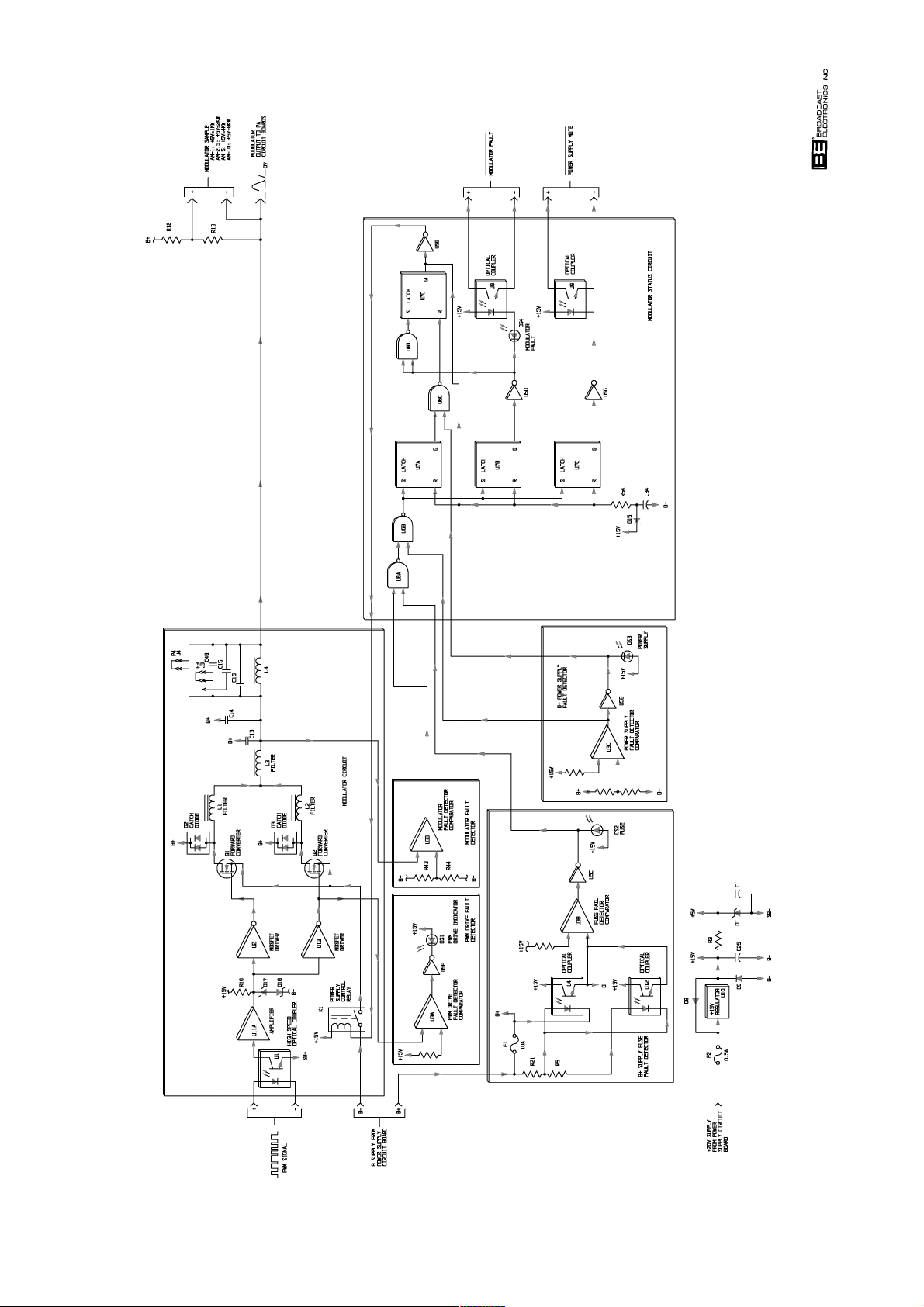
597-1112-26
COPYRIGHT © 1997 BROADCAST ELECTRONICS, INC
FIGURE 1-1. MODULATOR CIRCUIT BOARD
SIMPLIFIED SCHEMATIC
(1-3/1-4)
Page 27

1-18. RF AMPLIFIER CIRCUIT BOARD.
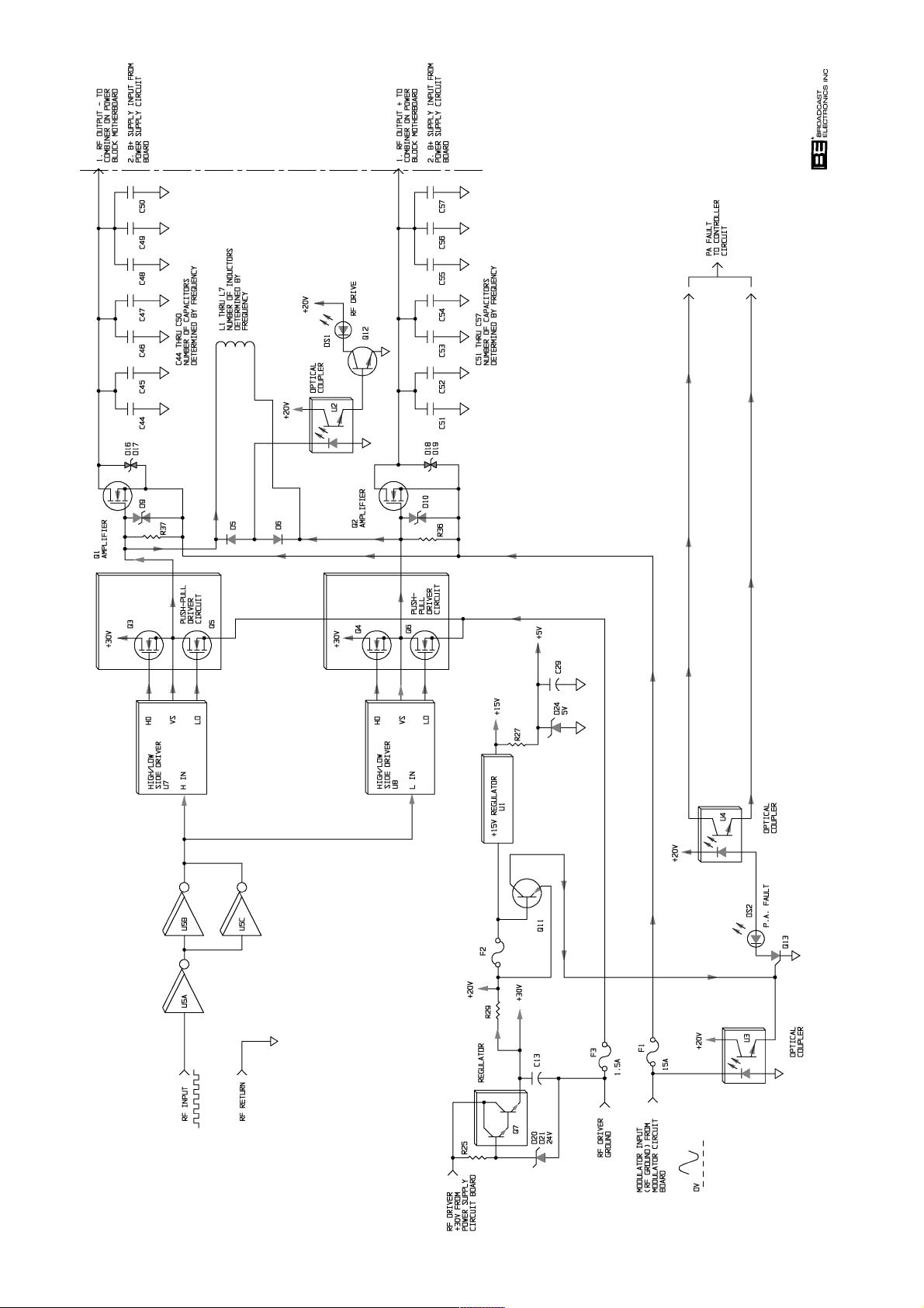
1-19. Each RF power module is equipped with two RF amplifier circuit boards: 1) power amplifiĆ
er 1 and 2) power amplifier 2. The circuit boards are designed with Class E power amplifier circuitry. Each circuit board is designed to produce approximately 550 watts of RF
power. Figure 1-2 presents the RF amplifier circuit board circuitry. The RF amplifier
circuit boards are identical, therefore only power amplifier 1 will be explained.
1-20.
1-21. The output from U5A is applied through inverters U5B/U5C to high/low side driver U7
1-22.
1-23.
PRE-DRIVER CIRCUIT. A +15 volt peak-to-peak square-wave signal at the carrier freĆ
quency is applied to a transformer on the power block motherboard assembly. The transĆ
former outputs two signals to inverter U5A.
and U8. U7/U8 output high and low drive signals to driver circuit transistors Q3/Q5 and
Q4/Q6.
DRIVER CIRCUIT. The driver circuit consists of: 1) transistors Q3 and Q5 and 2) Q4 and
Q6. Q3/Q5 and Q4/Q6 are MOSFET transistors configured as a push-pull driver circuit.
The outputs of Q3/Q5 and Q4/Q6 are applied to MOSFET power transistors Q1 and Q2.
Operating potentials for the driver circuitry is provided by the RF driver +30 volt supply.
The supply is protected from over-voltage conditions by a regulator Q7. The regulator
limits the voltage to approximately 47 volts dc. Fuse F2 protects the +30 volt supply from
over-current conditions. Fuse F3 protects the driver circuit components from over-current conditions.
RF AMPLIFIER CIRCUIT. The RF amplifier circuit consists of switching MOSFET transisĆ
tors Q1 and Q2. Q1 and Q2 are configured as a Class E switching amplifier network.
Class E power amplifier characteristics consist of: 1) the transistor drain-to-source voltĆ
age must be nominally zero immediately prior to the turn-on of the transistor and 2) the
time slope of the drain-to-source voltage waveform must be nominally zero prior to the
turn-on of the transistor. The Class E circuit results in: 1) reduced device dissipation
and lowers the transistor operating temperature which greatly increases the life of the
components, 2) an operating efficiency of 95% or greater, and 3) increased reliability when
operated into VSWR conditions.
1-24. Additional characteristics of a Class E amplifier design is the application of dc power to
the amplifier transistors. The B+ and B- supplies are applied to RF choke L1 on the comĆ
biner assembly. The choke is connected to the primary center tap winding of combiner
transformer T1. The transistors are connected to the primary winding of the transformers. The B- supply for the power amplifier is provided by the modulator circuit board.
The modulator outputs a dc voltage which varies with audio modulation and functions as
the RF ground for transistors Q1 and Q2. The RF ground potential will change in response to the applied audio. Fuse F1 protects the power amplifiers from over-current
conditions.
1-25. Transistors Q1 and Q2 operate together to generate approximately 550 watts of RF power.
Q1 operates 180 degrees out-of phase with transistor Q2. Inductors L1 through L7 imĆ
prove the efficiency of the drive circuit by storing the energy required to charge the input
capacitance of the transistors. Transzorbs D9/D10 prevent the gates of Q1/Q2 from damĆ
age by transients during power on and off. Capacitors C 44 through C50 and C51 through
C57 provide shaping for the Class E waveform. The RF power from power amplifier 1 is
combined with the 550 watts of RF power from power amplifier circuit board 2 at a combiner transformer on the power block motherboard assembly to generate 1100 watts of RF
power.
1-5
Page 28

1-26. RF DRIVE STATUS CIRCUIT. The RF drive signal is monitored by an RF drive status cirĆ
cuit. When an RF drive signal is present, a sample of the RF drive signal is rectified by
diodes D5/D6. The voltage from D5/D6 is applied to optical coupler U2. The output of U2
will go HIGH and bias transistor Q12 on. The output of Q12 will go LOW to illuminate
RF drive status indicator DS1.
1-27.
1-28. The fault detector functions by monitoring fuses F1 and F2. When fuse F2 is blown, tranĆ
1-29.
FAULT DETECTOR CIRCUIT. The power amplifier circuit board circuitry is monitored for
fault conditions by a fault detector circuit. The circuit is designed to monitor two operaĆ
tions: 1) the +30 volt supply and 2) the modulator output voltage (RF ground). The modulator output is monitored by optical coupler U3. The +20 volt supply is monitored by
transistor Q11. The power amplifier is protected from over-current conditions by fuse F1.
The +30 volt supply is protected from over-current conditions by fuse F2.
sistor Q11 will output +20 volts to silicon-controlled-rectifier (SCR) Q13. When fuse F1 is
blown, optical coupler U3 will output +20 volts to SCR Q13. When either voltage is presĆ
ent, the voltage will bias Q13 on to illuminate PA fault indicator DS2 and bias optical couĆ
pler U4 on. U4 will respond by routing a PA fault signal to the controller circuit board.
POWER SUPPLY CIRCUIT. An operating potential for the amplifier circuit board circuit-
ry is provided by the +30 volt supply from the power supply circuit board. The supply is
protected from over-current conditions by fuse F2. The +30 supply is regulated into a:
1) +15 volt supply by U1 and 2) +20 volt supply by R29. U1 is a three-terminal adjustable
regulator containing internal thermal and short-circuit current limiting features. Fuse
F2 protects the +30 volt supply from over-current conditions. Fuse F1 protects the power
amplifier components from over-current conditions. Fuse F3 protects the driver circuit
components from over-current conditions.
1-6
Page 29
597-1112-27
(1-7/1-8)
CIRCUIT BOARD
SIMPLIFIED SCHEMATIC
COPYRIGHT © 1997 BROADCAST ELECTRONICS, INC
FIGURE 1-2. POWER AMPLIFIER
Page 30

SECTION II
RF POWER MODULE MAINTENANCE
2-1. INTRODUCTION.
2-2. This section provides maintenance information for the AM-10A/AM-6A transmitter RF
power modules.
2-3.
SAFETY CONSIDERATIONS.
WARNING
THE TRANSMITTER CONTAINS MULTIPLE CIRCUIT
GROUNDS WITH HIGH AC AND DC POTENTIALS
WARNING
WARNING
WARNING
WITH RESPECT TO THE CABINET WHICH IS AT
EARTH POTENTIAL. DO NOT ENERGIZE THE
TRANSMITTER WITH TEST EQUIPMENT CONĆ
NECTED TO THE TRANSMITTER OUTPUT
NETWORK, RF POWER MODULE, RF COMBINER, OR
POWER SUPPLY COMPONENTS.
2-4. The AM-10A/AM-6A transmitters contain high voltages and currents. If safety
precautions are not practiced, contact with the high voltages and currents could cause
serious injury or death. The transmitter is equipped with many built-in safety features,
however good judgement, care, and common sense must be practiced to prevent accidents.
2-5. In addition to high voltages and currents, the transmitters contain multiple circuit
grounds with high ac and dc potentials with respect to the cabinet which is at earth
potential. The potentials could cause serious injury or death if maintenance personnel
simultaneously touch a circuit ground and the cabinet. As a result, operation of the
transmitter with test equipment connected to transmitter output network, RF power
module, RF combiner, or power supply components is extremely dangerous and must not
be attempted. Therefore, never energize the transmitter with test equipment connected to
the transmitter output network, RF power module, RF combiner, or power supply
components. Test equipment may be connected to the ECU circuit boards from the front
of the transmitter using the supplied extender circuit board with power energized. The
maintenance procedures presented in this section should be performed only by trained
and experienced maintenance personnel.
2-6.
2-7. First level maintenance consists of precautionary procedures applied to the equipment to
2-8.
FIRST LEVEL MAINTENANCE.
prevent future failures. The procedures are performed on a regular basis and the results
recorded in a performance log.
CLEANING AND INSPECTION.
2-1
WARNING: DISCONNECT POWER PRIOR TO SERVICING
Page 31
WARNING
WARNING
DISCONNECT ALL TRANSMITTER PRIMARY POWER
BEFORE ATTEMPTING ANY EQUIPMENT MAINTEĆ
NANCE.
CAUTION
REMOVING OR INSTALLING AN RF POWER MODULE
WITH THE TRANSMITTER ENERGIZED MAY RESULT
CAUTION
IN DAMAGE TO THE MODULE.
DO NOT REMOVE THE
RF POWER MODULES WITH THE TRANSMITTER ENĆ
ERGIZED.
2-9. Ensure all transmitter primary power is disconnected and remove an RF power module.
Clean the module of accumulated dust as required using a nylon bristle brush and
vacuum cleaner. Inspect the circuit boards for improperly seated semiconductors and
components damage by overheating. In addition, inspect the module for loose hardware.
Repeat the procedure for each module in the transmitter.
2-10.
2-11. Second level maintenance is the performance of procedures required to restore an RF
2-12.
SECOND LEVEL MAINTENANCE.
power module to operation after a fault has occurred. The RF power modules contain no
electrical adjustments. Therefore, the following text presents only troubleshooting
procedures.
TROUBLESHOOTING.
WARNING
THE TRANSMITTER CONTAINS MULTIPLE CIRCUIT
GROUNDS WITH HIGH AC AND DC POTENTIALS
WARNING
WARNING
WARNING
WITH RESPECT TO THE CABINET WHICH IS AT
EARTH POTENTIAL. DO NOT ENERGIZE THE
TRANSMITTER WITH TEST EQUIPMENT CONĆ
NECTED TO THE TRANSMITTER OUTPUT
NETWORK, RF POWER MODULE, RF COMBINER, OR
POWER SUPPLY COMPONENTS.
CAUTION
REMOVING OR INSTALLING AN RF POWER MODULE
WITH THE TRANSMITTER ENERGIZED MAY RESULT
CAUTION
IN DAMAGE TO THE MODULE.
DO NOT REMOVE THE
RF POWER MODULES WITH THE TRANSMITTER ENĆ
ERGIZED.
2-13. SAFETY CONSIDERATIONS. The AM-10A/AM-6A transmitters are equipped with
extensive indicator and meter circuitry to allow the operator to isolate problems to a
specific area within the transmitter. Due to the hazardous voltages and currents
contained in the equipment, operation of the transmitter with test equipment connected
to transmitter output network, RF power module, RF combiner, or power supply
components is extremely dangerous and must not be attempted. Test equipment may be
connected to the ECU circuit boards from the front of the transmitter using the supplied
extender circuit board with power energized. The maintenance procedures presented in
this section should be performed only by trained and experienced maintenance personnel.
2-2
WARNING: DISCONNECT POWER PRIOR TO SERVICING
Page 32

2-14. The RF power modules are not designed to be removed from the cabinet with the power
energized. Therefore, operate the transmitter to off before removing an RF power module
from the cabinet for maintenance procedures.
2-15.
RF POWER MODULE ASSEMBLY PROCEDURE. In the event of a failure in an RF power
module, the module will be required to be disassembled. The module must be properly
re-assembled to prevent circuit board and connector mis-alignment. To re-assemble an
RF power module, proceed as follows:
1. Locate the PA 2 circuit board and install the hex standoffs in the four locations at
the rear of the circuit board.
2. Locate the PA 1 circuit board and install the front panel mounting bracket using
the four Phillips-head screws. Do not secure the screws at this time. Repeat the
procedure for the PA2 circuit board and the modulator circuit board.
3. Install the PA 1 circuit board in the PA 1 location on the RF power module front
panel. Secure the circuit board bracket to the front panel using the hex nuts.
Repeat the procedure for the PA 2 and modulator circuit boards.
4. Place the RF power module on a square and flat surface such as a table with the
top of the module facing up.
5. Place the module front panel flush with the edge of the table and align the circuit
boards as follows:
A. Move the PA 1 circuit board until the front of the circuit board is flush with the
RF module front panel and the top edge of the circuit board is straight.
B. Secure the two Phillips-head screws which mount the circuit board to the
bracket.
2-16.
2-17.
2-18.
C. Repeat the procedure for the PA 2 and modulator circuit boards.
6. Rotate the module and repeat the alignment procedure for the bottom circuit board
bracket screws. Secure the two Phillips-head screws mounting the circuit board
to the bracket when each circuit board is properly aligned.
7. Install the hardware securing the PA 1 circuit board and the modulator circuit
board to the standoffs.
RF POWER MODULE EXCHANGE PROGRAM. If an RF power module is determined to
be defective, Broadcast Electronics has established an RF power module exchange
program. The program allows the customer to exchange a defective module for a
re-conditioned module. Terms of the program are available from the Broadcast
Electronics Customer Service Department. If an RF power module is determined to be
defective, troubleshoot the module or contact the Broadcast Electronics Customer Service
department for terms of the module exchange program.
TROUBLESHOOTING PROCEDURES. The RF power module troubleshooting procedures
are presented in Table 2-1. During the execution of the procedures, perform all
troubleshooting procedures for a symptom. The symptom may contain multiple
component failures. Once the trouble is isolated, refer to the circuit board theory of
operation and schematic diagrams to assist in problem resolution.
COMPONENT REPLACEMENT PROCEDURE. Component replacement procedures for
the RF power modules are presented in PART I SECTION V. Refer to COMPONENT
REPLACEMENT in SECTION V as required for the replacement procedures.
2-3
WARNING: DISCONNECT POWER PRIOR TO SERVICING
Page 33
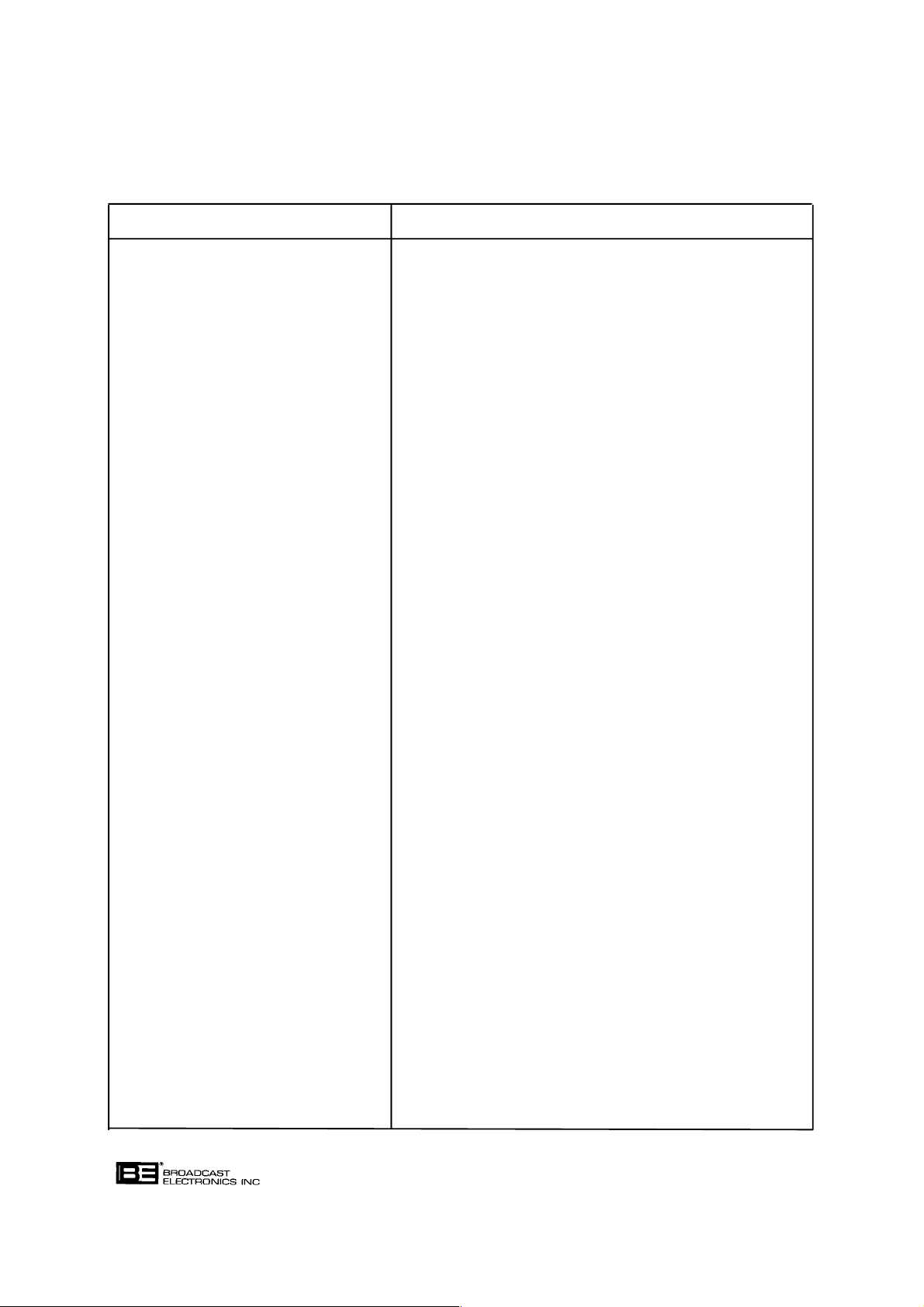
TABLE 2-1. RF POWER MODULE TROUBLESHOOTING
(Sheet 1 of 3)
SYMPTOM CIRCUITRY TO CHECK
RF DRIVE INDICATOR 1. Determine transistor reference voltages of a
EXTINGUISHED OR FLICKERING power amplifier with no faults as follows:
OR FAULT INDICATOR A. Remove an operational power amplifier with no
ILLUMINATED faults from an RF power module.
B. Using a digital voltmeter, operate the
voltmeter to diode check and determine a
reference voltage for the transistors on the
circuit board as follows:
1. Place the negative lead on the drain of Q1
(center pin) and the positive lead on the gate
and determine the voltage. The voltage using a
Fluke 77 meter = .45.
2. Place the negative lead on the drain of Q1
and the positive lead on the source and
determine the voltage. The voltage using a
Fluke 77 meter = .45.
2. Using the voltmeter as described in the preceding
step, measure the drain-to-gate and
drain-to-source voltage of transistor Q1 on the
defective power amplifier circuit board.
A. If the voltage is greater than ±0.1 volt of
the reference, defective Q1, Q3, and Q5.
B. If the voltage is equal to the reference, repeat
the preceding step for transistor Q2 on
the defective power amplifier circuit board.
3. Using a digital voltmeter, operate the voltmeter
to diode check and troubleshoot transistor Q3 as
follows:
A. Place the negative lead on the drain of Q3
(center pin) and the positive lead on the gate
and determine if a short circuit condition is
present.
B. Place the negative lead on the drain of Q3
and the positive lead on the source and
determine if a short circuit condition is
present.
C. If a short circuit condition is present, defective
Q3.
4. Repeat the procedure for transistors Q4, Q5, and
Q6.
5. Visually inspect regulator U1 for broken leads.
6. Check and replace all blown fuses on the circuit
board.
2-4
WARNING: DISCONNECT POWER PRIOR TO SERVICING
Page 34
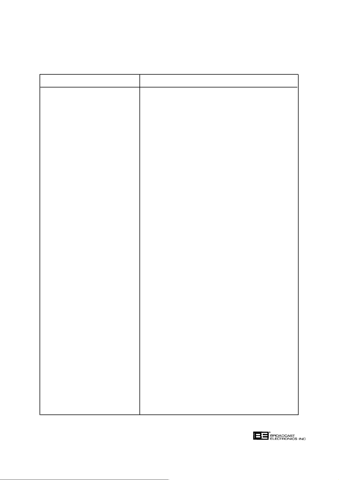
TABLE 2-1. RF POWER MODULE TROUBLESHOOTING
(Sheet 2 of 3)
SYMPTOM CIRCUITRY TO CHECK
MOD PWM DRIVE INDICATOR 1. Refer to RF DRIVE INDICATOR
EXTINGUISHED AND FAULT EXTINGUISHED OR FLICKERING OR FAULT
OR FUSE INDICATOR INDICATOR ILLUMINATED in the preceding
ILLUMINATED text and troubleshoot the power amplifier circuit
board.
2. If no defective circuitry is located on the power
amplifier circuit board, refer to FAULT OR FUSE
INDICATOR ILLUMINATED in the following
text and troubleshoot the modulator circuit
board.
MOD PWM DRIVE INDICATOR 1. Defective U2 or U13 on the modulator circuit board.
EXTINGUISHED
FAULT OR FUSE INDICATOR 1. Visually inspect regulator U10 for broken leads.
ILLUMINATED 2. Determine transistor reference voltages of a
modulator circuit board with no faults as
follows:
A. Remove a modulator with no faults from
an RF power module.
B. Using a digital voltmeter, operate the
voltmeter to diode check and determine a
reference voltage for the transistors on the
circuit board as follows:
1. Place the negative lead on the drain of Q1
(center pin) and the positive lead on the gate
and determine the voltage. The voltage using a
Fluke 77 meter = 1.2V.
2. Place the negative lead on the drain of Q1
and the positive lead on the source and
determine the voltage. The voltage using a
Fluke 77 meter = .46V.
3. Using the voltmeter as described in the preceding
step, measure the drain-to-gate and
drain-to-source voltage of transistor Q1 on the
defective modulator circuit board.
A. If the voltage is greater than ±0.1 volt of
the reference, proceed as follows:
1. Remove the wire from terminal E1.
2. Using the voltmeter as described in the
preceding text, measure the drain-to-gate and
drain-to-source voltage of transistor Q1 on
the defective modulator circuit board.
B. If the voltage at Q1 is greater than ± 0.1V of
the reference, defective Q1.
C. If the voltage at Q1 is equal to the reference,
defective Q2.
2-5
WARNING: DISCONNECT POWER PRIOR TO SERVICING
Page 35
TABLE 2-1. RF POWER MODULE TROUBLESHOOTING
(Sheet 3 of 3)
SYMPTOM CIRCUITRY TO CHECK
FAULT OR FUSE INDICATOR 4. Replace all blown fuses on the circuit board.
ILLUMINATED (CONT'D) 5. Re-install the modulator circuit board and install
the RF module in the transmitter. If the
modulator remains defective, replace U2 and U13.
6. If the modulator remains defective, contact the
Broadcast Electronics Customer Service
Department.
2-6
WARNING: DISCONNECT POWER PRIOR TO SERVICING
Page 36

SECTION III
RF POWER MODULE
PARTS LIST
3-1. INTRODUCTION.
3-2. This section provides descriptions and part numbers of electrical components, assemblies,
and selected mechanical parts required for maintenance of the RF Power Module. Each
table entry in this section is indexed by reference designators appearing on the applicable
schematic.
TABLE 3-1. REPLACEABLE PARTS LIST INDEX
TABLE DESCRIPTION PART NO. PAGE
3-2 Power Module Assembly 957-0010-001 3-2
3-3 Modulator Circuit Board Assembly 917-0302 3-2
3-4 Power Amplifier Circuit Board Assembly 917-0304 3-5
3-5 Power Module Frequency Dependant Kit, 522 - 650 kHz 957-1015-001 3-8
3-6 Power Module Frequency Dependant Kit, 651 - 770 kHz 957-1015-002 3-8
3-7 Power Module Frequency Dependant Kit, 771 - 920 kHz 957-1015-003 3-8
3-8 Power Module Frequency Dependant Kit, 921 - 1080 kHz 957-1015-004 3-8
3-9 Power Module Frequency Dependant Kit 1081 - 1300 kHz 957-1015-005 3-9
3-10 Power Module Frequency Dependant Kit 1301 - 1580 kHz 957-1015-006 3-9
3-11 Power Module Frequency Dependant Kit, 1581 - 1700 kHz 957-1015-007 3-9
3-1
Page 37

TABLE 3-2. POWER MODULE ASSEMBLY - 957-0010-001
REF. DES. DESCRIPTION PART NO. QTY.
---- Modulator Circuit Board Assembly 917-0302 1
---- Power Amplifier Circuit Board Assembly 917-0304 2
TABLE 3-3. MODULATOR CIRCUIT BOARD ASSEMBLY - 917-0302
(Sheet 1 of 4)
REF. DES. DESCRIPTION PART NO. QTY.
C1 Capacitor, Electrolytic, 10 uF, 50V 023-1076 1
C2 Capacitor, Monolythic Ceramic, .1 uF ±10%, 100V 003-1041 1
C3 Capacitor, Electrolytic, 22 uF, 50V 024-2274 1
C4 Capacitor, Monolythic Ceramic 1 uF ±10%, 100V 003-1041 1
C5 Capacitor, Electrolytic, 330 uF, 200V dc 013-3385-201 1
C6 Capacitor, Polypropylene Film, .47 uF, 250V, Oval 033-4743 1
C7 Capacitor, Mica, 1000 pF ±10%, 350V 046-0002 1
C8 Capacitor, Electrolytic, 330 uF, 200V dc 013-3385-201 1
C9 Capacitor, Polypropylene Film, .47 uF, 250V, Oval 033-4743 1
C10 Capacitor, Mica, 1000 pF ±10%, 350V 046-0002 1
C11, C12 Capacitor, Monolythic Ceramic, .1 uF ±10%, 100V 003-1041 2
C13, C14 Capacitor, Polypropylene Film, 2.2 uF, 400V 030-2256 2
C15, C16 Capacitor, Metallized Polypropylene Film, .068 uF ±10%, 250V 030-6843 2
C17 Capacitor, Monolythic Ceramic, .1 uF ±10%, 100V 003-1041 1
C18, C19 Capacitor, Electrolytic, 10 uF, 50V 023-1076 2
C20 Capacitor, Monolythic Ceramic, .1 uF ±10%, 100V 003-1041 1
C21 Capacitor, Ceramic, 0.001 uF ±10%, 200V 030-1033 1
C22 Capacitor, Electrolytic, 10 uF, 50V 023-1076 1
C23 Capacitor, Electrolytic, 22 uF, 50V 024-2274 1
C24 Capacitor, Electrolytic, 10 uF, 50V 023-1076 1
C25 Capacitor, Electrolytic, 22 uF, 50V 024-2274 1
C26, C27 Capacitor, Monolythic Ceramic, .1 uF ±10%, 100V 003-1041 2
C28 thru C32 Capacitor, Electrolytic, 10 uF, 50V 023-1076 5
C33 Capacitor, Monolythic Ceramic, .1 uF ±10%, 100V 003-1041 1
C34 Capacitor, Electrolythic, 47 uF, 35V 020-4773 1
C35 Capacitor, Electrolytic, 10 uF, 50V 023-1076 1
C36, C37 Capacitor, Ceramic, 0.001 uF ±10%, 200V 030-1033 2
C38, C39 Capacitor, Monolythic Ceramic, .1 uF ±10%, 100V 003-1041 2
C40 Capacitor, Electrolytic, 10 uF, 50V 023-1076 1
C41 Capacitor, Electrolytic, 33 uF, 25V 020-3374 1
C42 Capacitor, Polypropylene Film, 2.2 uF, 400V 030-2256 1
C43 Capacitor, Polypropylene Film, .47 uF, 250V, Oval 033-4743 1
C44 Capacitor, Polypropylene Film, .033 uF, ±10%, 200V 030-3353 1
C45 Capacitor, Mica, 820 pF ±5%, 300V 042-8222 1
C46, C47 Capacitor, Monolythic Ceramic, .1 uF ±10%, 100V 003-1041 2
C48 Capacitor, Metallized Polypropylene Film, .068 uF ±10%, 250V 030-6843 1
3-2
Page 38

TABLE 3-3. MODULATOR CIRCUIT BOARD ASSEMBLY 917-0302
(Sheet 2 of 4)
REF. DES. DESCRIPTION PART NO. QTY.
C49 Capacitor, Polypropylene Film, .033 uF ±10%, 200V 030-3353 1
C50 Capacitor, Mylar, 0.01 uF ±10%, 100V 031-1043 1
D1 Diode, Zener, 1N4733A, 5.1V ±5%, 1W 200-4733 1
D2, D3 Diode, Fast Recovery, 16JPF20 200-1620 2
D4 Diode, 1N4005, Silicon, 600V @ 1 Ampere 203-4005 1
D5 Diode, 1N4148, Silicon, 75V @ 0.3 Amperes 203-4148 1
D6 Diode, 1N4005, Silicon, 600V @ 1 Ampere 203-4005 1
D7 Diode, Zener, 1N4739A, 9.1V ±5%, 1W 200-0009 1
D8, D9 Diode, 1N4005, Silicon, 600V @ 1 Ampere 203-4005 2
D10 Diode, 1N6276A, Silicon, Transient Voltage Suppressor, 206-6276 1
16V ±0.05% Breakdown
D11 Switchmode Power Rectifier, MUR460 230-0014 1
D12, D13 Diode, 1N4148, Silicon, 75V @ 0.3 Amperes 203-4148 2
D14, D15 Diode, 1N4005, Silicon, 600V @ 1 Ampere 203-4005 2
D16 Diode, 1N4148, Silicon, 75V @ 0.3 Amperes 203-4148 1
D17 Diode, Zener, 1N4739A, 9.1V ±5%, 1W 200-0009 1
D18 Diode, Zener, 1N4728, 3.3V ±5%, 1W 201-4728 1
D19 Diode, 1N4005, Silicon, 600V @ 1 Ampere 203-4005 1
D20 thru D23 Diode, 1N4148, Silicon, 75V @ 0.3 Amperes 203-4148 4
D24,D25 Diode, 1N5817, Schottky, 20V @ 1 Amperes 200-0019 2
DS1 Indicator, LED, Green, 521-9175, 3V @ 40 mA Maximum 323-9224 1
DS2 Indicator, LED, Red, 521-9212, 1.7V @ 50 mA Maximum 323-9217 1
DS3 Indicator, LED, Green, 521-9175, 3V @ 40 mA Maximum 323-9224 1
DS4 Indicator, LED, Red, 521-9212, 1.7V @ 50 mA Maximum 323-9217 1
F1 Fuse, 3AG, 20 Amperes, 250V 330-2000 1
F2 Fuse, AGC, 1 Ampere, MDL, 250V, Slow-Blow 334-0100 1
J3, J4 Jumper, Programmable, 2-Pin 340-0004 2
K1 Relay, SPST, 30 Amperes 270-1213 1
P2 Connector, 15-Pin, SUB-D, Male, Right Angle 417-0374 1
P3 Receptacle, Male, 3-Pin In-line 417-0003 1
P4 Receptacle, Male, 2-Pin In-line 417-4004 1
Q1, Q2 Modulator, FET MTY55N20E, 200V, 55 Amperes 210-0550 2
R1 Resistor, 1.33 k Ohm ±1%, 1/4W 103-1331 1
R2 Resistor, 470 Ohm ±5%, 1/2W 110-4733 1
R3 Resistor, 332 Ohm ±1%, 1/4W 103-3323 1
R4 Resistor, 1 Ohm ±5%, 1/4W 100-1013 1
R5 Resistor, 10 k Ohm ±1%, 1/4W 100-1051 1
R7 Resistor, 12k Ohm, 2W, ±5% 130-1253 1
R8 Resistor, 3.3 Meg Ohm ±5%, 1/4W 100-3373 1
R9 Resistor, 10 Ohm ±1%, 1/4W 103-1021 1
R10 Resistor, 3.65 k Ohm ±1%, 1/4W 103-3641 1
R11 Resistor, 10 Ohm ±1%, 1/4W 103-1021 1
R12 Resistor, 453 k Ohm ±1%, 1/4W 100-4561 1
R13 Resistor, 130 k Ohm ±1%, 1/4W 103-1306 1
R14 Resistor, 1 k Ohm ±1%, 1/4W 100-1041 1
3-3
Page 39

TABLE 3-3. MODULATOR CIRCUIT BOARD ASSEMBLY 917-0302
(Sheet 3 of 4)
REF. DES. DESCRIPTION PART NO. QTY.
R15 Resistor, 332 k Ohm ±1%, 1/4W 103-3326 1
R16 Resistor, 69.8 k Ohm ±1%, 1/4W 103-6985 1
R17 Resistor, 2.21 k Ohm ±1%, 1/4W 103-2241 1
R18 Resistor, 10 k Ohm ±1%, 1/4W 100-1051 1
R19 Resistor, 3.65 k Ohm ±1%, 1/4W 103-3641 1
R20 Resistor, 1 k Ohm ±1%, 1/4W 100-1041 1
R21 Resistor, 27 k Ohm ±5%, 1W 120-2753 1
R22 Resistor, 22.1 k Ohm ±1%, 1/4W 103-2211 1
R23 Resistor, 10 k Ohm ±1%, 1/4W 100-1051 1
R24 Resistor, 332 k Ohm ±1%, 1/4W 103-3326 1
R25 Resistor, 2.21 k Ohm ±1%, 1/4W 103-2241 1
R26 Resistor, 1 k Ohm ±1%, 1/4W 100-1041 1
R27 Resistor, 100 k Ohm ±1%, 1/4W 103-1062 1
R28 Resistor, 69.8 k Ohm ±1%, 1/4W 103-6985 1
R29 Resistor, 3.65 k Ohm ±1%, 1/4W 103-3641 1
R30 Resistor, 10 k Ohm ±1%, 1/4W 100-1051 1
R31 Resistor, 332 k Ohm ±1%, 1/4W 103-3326 1
R32 Resistor, 2.21 k Ohm ±1%, 1/4W 103-2241 1
R33 Resistor, 1 k Ohm ±1%, 1/4W 100-1041 1
R34 Resistor, 121 Ohm ±1%, 1/4W 100-1231 1
R35 Resistor, 1.33 k Ohm ±1%, 1/4W 103-1331 1
R38 Resistor, 47.5 k Ohm ±1%, 1/4W 103-4755 1
R39 Resistor, 1 k Ohm ±1%, 1/4W 100-1041 1
R40 Resistor, 1 k Ohm ±1%, 1/4W 100-1041 1
R41 Resistor, 100 k Ohm ±1%, 1/4W 103-1062 1
R42 Resistor, 8.66 k Ohm ±1%, 1/4W 100-8641 1
R43 Resistor, 499 k Ohm ±1%, 1/4W 103-4996 1
R44 Resistor, 8.25 k Ohm ±1%, 1/4W 103-8254 1
R45 Resistor, 1 k Ohm ±1%, 1/4W 100-1041 1
R46 Resistor, 1 Meg Ohm ±1%, 1/4W 103-1007 1
R47 thru R49 Resistor, 10 k Ohm ±1%, 1/4W 100-1051 3
R51 Resistor, 15.4 k Ohm ±1%, 1/4W 103-1551 1
R52 Resistor, 39 Ohm ±5%, 1/2W 110-3923 1
R53 Resistor, 3.3 Meg Ohm ±
R54, R55 Resistor, 100 Ohm ±1%, 1/4W 100-1031 2
R56, R57 Resistor, 3.3 Meg Ohm ±5%, 1/4W 100-3373 2
R58 Resistor, 453 k Ohm ±1%, 1/4W 100-4561 1
TP1 thru TP4 Terminal, Test Point, Oval, Red 413-0106 4
TP5, TP6 Jack, Test, Right Angle Printed Circuit Board Mount 417-0004 2
U1 Integrated Circuit, Opto-Isolator, 6N137 220-6137 1
U2 Driver, TC4421CAT, 2 Ampere, 5-Pin, TO-220 Case 220-4421 1
U3 Integrated Circuit, LM339AN, Quad Comparator, 14-Pin DIP 221-0339 1
U4 Integrated Circuit, 4N33, Optical Isolator, NPN Photo 229-0033 1
Transistor/Infared Emitting Diode Type, 1500V Isolation,
Response: 30 kHz Maximum, Current: 50 mA Maximum, 6-Pin DIP
5%, 1/4W 100-3373 1
3-4
Page 40

TABLE 3-3. MODULATOR CIRCUIT BOARD ASSEMBLY 917-0302
(Sheet 4 of 4)
REF. DES. DESCRIPTION PART NO. QTY.
U5 Integrated Circuit, ULN2004, 7 NPN Darlington Driver Pack, 226-2004 1
16-Pin DIP
U6 Integrated Circuit, MC14093B, Quad 2-Input NAND Schmitt Trigger, 220-4093 1
CMOS, 14-Pin DIP
U7 Integrated Circuit, MC14044BP, Quad NAND R-S Latch, CMOS, 228-4044 1
16-Pin DIP
U8, U9 Integrated Circuit, 4N33, Optical Isolator, NPN Photo 229-0033 2
Transistor/Infared Emitting Diode Type, 1500V Isolation,
Response: 30 kHz Maximum, Current: 50 mA Maximum, 6-Pin DIP
U10 Integrated Circuit, LM317T, Adjustable Positive Voltage 227-0317 1
Regulator, 1.2V to 37V, 1.5 Ampere, TO-220 Case
U11 Integrated Circuit, 14505, Hex Level Shifter, TTL to CMOS, 228-4504 1
16-Pin DIP
U12 Integrated Circuit, 4N33, Optical Isolator, NPN Photo 229-0033 1
Transistor/Infared Emitting Diode Type, 1500V Isolation,
Response: 30 kHz Maximum, Current: 50 mA Maximum, 6-Pin DIP
U13 Driver, TC4421CAT, 2 Ampere, 5-Pin, TO-220 Case 220-4421 1
XF1, XF2 Fuse Clips, AGC 415-2068 2
XU1 Socket, 8-Pin DIP 417-0804 1
XU3 Socket, 14-Pin DIP 417-1404 1
XU4 Socket, 6-Pin DIP 417-0600 1
XU5 Socket, 16-Pin DIP 417-1604 1
XU6 Socket, 14-Pin DIP 417-1404 1
XU7 Socket, 16-Pin DIP 417-1604 1
XU8, XU9 Socket, 6-Pin DIP 417-0600 2
XU11 Socket, 16-Pin DIP 417-1604 1
XU13 Socket, 6-Pin DIP 417-0600
---- Coil, 36 uH, MOD PWM 360-0108 2
---- Coil, 9.2 uH, MOD PWM 360-0109 1
---- Coil, 14 uH, MOD PWM 360-0110 1
---- Blank, Modulator Circuit Board 517-0302 1
1
TABLE 3-4. POWER AMPLIFIER CIRCUIT BOARD ASSEMBLY - 917-0304
(Sheet 1 of 3)
REF. DES. DESCRIPTION PART NO. QTY.
C2 Capacitor, Monolythic Ceramic, 0.1 uF ±10%, 50V 003-1066 1
C3 thru C6 Capacitor, Monolythic Ceramic, 0.1 uF ±10%, 100V 003-1041 4
C8 Capacitor, Monolythic Ceramic, 0.1 uF ±10%, 50V 003-1066 1
C10 Capacitor, Electrolytic, 100 uF, 35V 023-1084 1
C11 Capacitor, Monolythic Ceramic, 0.1 uF ±10%, 50V 003-1066 1
C12 Capacitor, Monolythic Ceramic, 0.1 uF ±10%, 100V 003-1041 1
C13 Capacitor, Electrolytic, 100 uF, 63V 015-1084 1
C15 Capacitor, Monolythic Ceramic, 0.1 uF ±10%, 50V 003-1066 1
3-5
Page 41

TABLE 3-4. POWER AMPLIFIER CIRCUIT BOARD ASSEMBLY - 917-0304
(Sheet 2 of 3)
REF. DES. DESCRIPTION PART NO. QTY.
C16 thru C18 Capacitor, Ceramic, 0.001 uF ±10%, 200V 030-1033 3
C19 thru C21 Capacitor, Monolytic Ceramic, 0.1 uF ±10%, 50V 003-1066 3
C23 Capacitor, Mylar Film, 0.01 uF ±10%, 200V 030-1043 1
C24 Capacitor, Electrolytic, 10 uF, 50V 023-1076 1
C25 Capacitor, Electrolytic, 10 uF, 50V 023-1076 1
C26 Capacitor, Ceramic, 0.001 uF, 1 kV 002-1034 1
C27, C28 Capacitor, Monolythic Ceramic, 0.1 uF ±10%, 200V 003-1065 2
C29 thru Capacitor, Monolythic Ceramic, 0.1 uF ±10%, 100V 003-1041 4
C32
C33 Capacitor, Electrolytic, 10 uF, 50V 023-1076 1
C34 Capacitor, Monolythic Ceramic, 0.1 uF ±10%, 100V 003-1041 1
C36 ,C37 Capacitor, Mica, 39 pF ±5%, 500V 042-3912 2
C38, C39 Capacitor, Monolythic Ceramic, .47 uF ±10%, 50V 003-4743 2
C40 thru C43 Capacitor, Electrolytic, 1 uF, 50V 024-1064 4
C45 thru C55 Refer To Power Module Frequency Dependant Kit Tables After This Section.
C58 Capacitor, Monolythic Ceramic, .47 uF ±10%, 50V 003-4743 1
C59 Capacitor, Electrolytic, 10 uF, 50V 023-1076 1
D1 thru D6 Diode, 1N4148, Silicon, 75V @ 0.3 Amperes 203-4148 6
D9, D10 Transzorb Diode, 1N6281A, 27BV, 1.5KE27CA 206-0027 2
D11 Diode, Zener 1N5229, 4.3V, 0.5W 201-0035 1
D16 Diode, Transzorb, Diode, 300BV, 1.5FE300CA 206-0300 1
D17 Transzorb Diode, 250BV, 1.5KE250CA 206-0250 1
D18 Diode, Transzorb, Diode, 300BV, 1.5FE300CA 206-0300 1
D19 Transzorb Diode, 250BV, 1.5KE250CA 206-0250 4
D20, D21 Diode, Zener, 1N4749, 24V, 10.5 Amperes 200-0024 2
D22, D23 Diode, 1N4005, Silicon, 600V @ 1 Ampere 203-4005 2
D25, D26 Diode, 1N4148, Silicon, 75V @ 0.3 Amperes 203-4148 2
D29, D30 Diode, Zener, 1N4742A, 12V ±5%, 1W 200-4742 2
D31 Diode, Zener, 1N4737A, 7.5V, 1W, 34 mA 200-4737 1
D32 thru D35 Diode, 1N4148, Silicon, 75V @ 0.3 Amperes 203-4148 4
DS1 Indicator, LED, Green, 521-9175, 3V @ 40 mA Maximum 323-9224 1
DS2 Indicator, LED, Red, 521-9212, 1.7V @ 50 mA Maximum 323-9217 1
F1 Fuse, 3AB, 15 Amperes, 65V, Very Fast 330-1502 1
F2, F3 Fuse, 5 X 20MM, 1.5 Ampere, Slow-Blow 334-1150 2
FC1, FC2 Fuse Clips, AGC 415-2068 2
FC3 thru FC6 Fuse Clips, Littlefuse, 111501 415-2069 4
L1, L2 Coil, 4uH 360-0112 2
L3 thru L7 Refer To Power Module Frequency Dependant Kit Tables After This Section.
P2 Connector, 15-Pin Sub-D, Male, Right Angle 417-0374 1
Q1, Q2 RF FET, APT6018, 600V 210-6018 2
Q3 thru Q6 Hexfet Power Mosfet, IRFI520G, TO-220 Fullpak 210-0520 4
Q7 Transistor, TIP120, NPN Darlington-Connected Silicon 210-0120 1
Power, 65W @ 25#C Case
Q11 Transistor, 2N3906, PNP, Silicon, TO-92 Case 210-3906 1
Q12 Transistor, 2N3904, NPN, Silicon, TO-92 Case 211-3904 1
3-6
Page 42

TABLE 3-4. POWER AMPLIFIER CIRCUIT BOARD ASSEMBLY - 917-0304
(Sheet 3 of 3)
REF. DES. DESCRIPTION PART NO. QTY.
Q13 Silicon Controlled Rectifier, GE6CA, 100V @ 1.6 Ampere 237-0006 1
R1 Resistor, 1 k Ohm ±5%,1W 120-1043 1
R2, R3 Resistor, 10 k Ohm ±1%, 1/4W 100-1051 2
R4 Resistor, 100 Ohm ±1%, 1/4W 100-1031 1
R5 Resistor, 1.10 k Ohm ±1%, 1/4W 103-1104 1
R6, R7 Resistor, 10 k Ohm ±1%, 1/4W 100-1051 2
R8 thru R11 Resistor, 27 Ohm ±5%, 1/4W 100-2723 4
R12 Resistor, 15k Ohm ±5%, 2W 130-1553 1
R13 Resistor, 3.3 Meg Ohm ±5%, 1/4W 100-3373 1
R14 Resistor, 1.10 k Ohm ±1%, 1/4W 103-1104 1
R15 Resistor, 1 k Ohm ±5%, 1W 120-1043 1
R16 Resistor, 3.3 Meg Ohm ±5%, 1/4W 100-3373 1
R18 Resistor, 1.10 k Ohm ±1%, 1/4W 103-1104 1
R20 Resistor, 1.96 k Ohm ±1%, 1/4W 103-1964 1
R21, R22 Resistor, 10 k Ohm ±1%, 1/4W 100-1051 2
R23 Resistor, 10 Meg Ohm ±5%, 1/4W 100-1083 1
R24 Resistor, 1.96 k Ohm ±1%, 1/4W 103-1964 1
R25 Resistor, 680 Ohm ±5%, 1/2W 110-6833 1
R26 Resistor, 10 k Ohm ±1%, 1/4W 100-1051 1
R27, R28 Resistor, 332 Ohm ±1%, 1/4W 103-3323 1
R29 Resistor, 300 Ohm ±5%, 2W, W/W 130-3004 1
R30, R31 Resistor, 2.67 k Ohm ±1%, 1/4W 103-2674 2
R32, R33 Resistor, 100 Ohm ±1%, 1/4W 100-1031 2
R34, R35 Resistor, 10 k Ohm ±1%, 1/4W 100-1051 2
R36, R37 Resistor, 300 Ohm ±5%, 2W, W/W 130-3004 2
R38 Resistor, 562 Ohm ±1%, 1/4W 103-5623 1
R39, R40 Resistor, 10 k Ohm ±1%, 1/4W 100-1051 2
U1 Integrated Circuit, LM317T, Adjustable Positive Voltage 227-0317 1
Regulator, 1.2V to 37V, 1.5 Ampere, TO-220 Case
U2 thru U4 Integrated Circuit, 4N33, Optical Isolator, NPN Photo 229-0033 3
Transistor/Infared Emitting Diode Type, 1500V Isolation,
Response: 30 kHz Maximum, Current: 50 mA Maximum, 6-Pin DIP
U5 Integrated Circuit, MC14584, 14-Pin Schmitt 228-4584 1
U7, U8 Driver High and Low Side, IR2110 227-2110 2
XU2 thru XU4 Socket, 6-Pin DIP 417-0600 3
XU5, XU7, Socket, 14-Pin DIP 417-1404 3
XU8
---- Blank, Power Amplifier Circuit Board Assembly 517-0304 1
3-7
Page 43

TABLE 3-5. POWER MODULE FREQUENCY DEPENDANT KIT, 522 - 650 KHZ -
957-1015-001
REF. DES. DESCRIPTION PART NO. QTY.
C45, C56 Capacitor, Mica, 1600 pF, 1 kV 042-1622 4
C46 thru C55 Capacitor, Mica, 1800 pF, 1 kV 042-1832 20
L3, L4 Inductor, PA Drive 360-0113-XXX 4
---- Blank, PA Capacitor Board Circuit Board 517-0318-001 2
---- Blank, PA Inductor Board Circuit Board 517-0319-001 2
TABLE 3-6. POWER MODULE FREQUENCY DEPENDANT KIT, 651 - 770 KHZ -
957-1015-002
REF. DES. DESCRIPTION PART NO. QTY.
C46, C55 Capacitor, Mica, 1600 pF, 1 kV 042-1622 4
C47 thru C54 Capacitor, Mica, 1800 pF, 1 kV 042-1832 16
L3, L4 Inductor, PA Drive 360-0113-XXX 4
---- Blank, PA Capacitor Board Circuit Board 517-0318-001 2
---- Blank, PA Inductor Board Circuit Board 517-0319-001 2
TABLE 3-7. POWER MODULE FREQUENCY DEPENDANT KIT, 771 - 920 KHZ -
957-1015-003
REF. DES. DESCRIPTION PART NO. QTY.
C47 thru C54 Capacitor, Mica, 1800 pF, 1 kV 042-1832 16
L3, L4 Inductor, PA Drive 360-0113-XXX 4
---- Blank, PA Capacitor Board Circuit Board 517-0318-001 2
---- Blank, PA Inductor Board Circuit Board 517-0319-001 2
TABLE 3-8. POWER MODULE FREQUENCY DEPENDANT KIT, 921 - 1080 KHZ -
957-1015-004
REF. DES. DESCRIPTION PART NO. QTY.
C48, C53 Capacitor, Mica, 1600 pF, 1 kV 042-1622 4
C49 thru C52 Capacitor, Mica, 1800 pF, 1 kV 042-1832 8
C47, C54 Capacitor, Mica, 910 pF, 1 kV 042-9122 4
L5, L7 Inductor, PA Drive 360-0113-XXX 4
---- Blank, PA Capacitor Board Circuit Board 517-0318-001 2
---- Blank, PA Inductor Board Circuit Board 517-0319-001 2
3-8
Page 44

TABLE 3-9. POWER MODULE FREQUENCY DEPENDANT KIT, 1081 - 1300 KHZ -
957-1015-005
REF. DES. DESCRIPTION PART NO. QTY.
C48, C53 Capacitor, Mica, 1600 pF, 1 kV 042-1622 4
C49 thru C52 Capacitor, Mica, 1800 pF, 1 kV 042-1832 8
L5, L7 Inductor, PA Drive 360-0113-XXX 4
---- Blank, PA Capacitor Board Circuit Board 517-0318-001 2
---- Blank, PA Inductor Board Circuit Board 517-0319-001 2
TABLE 3-10. POWER MODULE FREQUENCY DEPENDANT KIT, 1301 - 1580 KHZ -
957-1015-006
REF. DES. DESCRIPTION PART NO. QTY.
C48, C53 Capacitor, Mica, 910 pF, 1 kV 042-9122 4
C49 thru C52 Capacitor, Mica, 1600 pF, 1 kV 042-1622 8
L5, L6, L7 Inductor, PA Drive 360-0113-XXX 6
---- Blank, PA Capacitor Board Circuit Board 517-0318-001 2
---- Blank, PA Inductor Board Circuit Board 517-0319-001 2
TABLE 3-11. POWER MODULE FREQUENCY DEPENDANT KIT, 1581 - 1700 KHZ -
957-1015-007
REF. DES. DESCRIPTION PART NO. QTY.
C49, C52 Capacitor, Mica, 1600 pF, 1 kV 042-1622 4
C50, C51 Capacitor, Mica, 1800 pF, 1 kV 042-1832 4
L5, L6, L7 Inductor, PA Drive 360-0113-XXX 6
---- Blank, PA Capacitor Board Circuit Board 517-0318-001 2
---- Blank, PA Inductor Board Circuit Board 517-0319-001 2
3-9
Page 45

SECTION IV
RF POWER MODULE DRAWINGS
4-1. INTRODUCTION.
4-2. This section provides assembly drawings, wiring diagrams, and schematic diagrams as
listed below for the Broadcast Electronics AM-10A/AM-6A transmitter RF power module.
FIGURE TITLE NUMBER
4-1 SCHEMATIC DIAGRAM, MODULATOR CIRCUIT BOARD SB917-0302
4-2 ASSEMBLY DIAGRAM, MODULATOR CIRCUIT BOARD AD917-0302
4-3 SCHEMATIC DIAGRAM, POWER AMPLIFIER CIRCUIT SB917-0304
BOARD
4-4 ASSEMBLY DIAGRAM, POWER AMPLIFIER CIRCUIT AD917-0304
BOARD
4–1
Page 46

TABLE OF CONTENTS
PARAGRAPH PAGE NO.
SECTION I OUTPUT NETWORK THEORY OF OPERATION
1-1 Introduction 1-1
1-3 Functional Description 1-1
SECTION II OUTPUT NETWORK MAINTENANCE
2-1 Introduction 2-1
2-3 Safety Considerations 2-1
2-6 First Level Maintenance 2-1
2-8 Cleaning and Inspection 2-1
2-10 Second Level Maintenance 2-2
2-12 Electrical Adjustments 2-2
2-13 Modulation Calibration Controls 2-2
2-14 Directional Coupler Null Controls 2-2
2-15 Troubleshooting 2-2
2-16 Safety Considerations 2-2
2-17 Output Network Assembly Component Locations 2-2
2-18 Troubleshooting Procedures 2-3
2-19 Component Replacement Procedure 2-3
SECTION III OUTPUT NETWORK ASSSEMBLY PARTS LIST
3-1 Introduction 3-1
SECTION IV OUTPUT NETWORK ASSEMBLY DRAWINGS
4-1 Introduction 4-1
LIST OF TABLES
TABLE TITLE PAGE NO.
2-1 DIRECTIONAL COUPLER CIRCUIT BOARD 2-3
TROUBLESHOOTING
2-2 LIGHTNING DETECTION CIRCUIT BOARD/ 2-3
SPARK GAP TROUBLESHOOTING
2-3 LIGHTNING PROTECTION CIRCUIT BOARD 2-3
TROUBLESHOOTING
3-1 REPLACEABLE PARTS LIST INDEX 3-1
Page 47

SECTION I
OUTPUT NETWORK THEORY OF OPERATION
1-1. INTRODUCTION.
1-2. This section presents the theory of operation for the AM-10A/AM-6A output network asĆ
sembly.
1-3.
1-4. The output network assembly contains the: 1) harmonic band-pass filter, 2) directional
FUNCTIONAL DESCRIPTION.
coupler circuit board, 3) lightning protection circuit board, 4) T-matching network,
5) lightning detection circuit board, and 6) spark gap. The theory of operation for the outĆ
put network assembly components is presented in PART I SECTION IV, THEORY OF OPĆ
ERATION. Refer to SECTION IV as required for a description of the output network asĆ
sembly components.
1-1
Page 48

SECTION II
OUTPUT NETWORK MAINTENANCE
2-1. INTRODUCTION.
2-2. This section provides maintenance information for the AM-10A/AM-6A transmitter
output network assembly.
2-3.
SAFETY CONSIDERATIONS.
WARNING
THE TRANSMITTER CONTAINS MULTIPLE CIRCUIT
GROUNDS WITH HIGH AC AND DC POTENTIALS
WARNING
WARNING
WARNING
WITH RESPECT TO THE CABINET WHICH IS AT
EARTH POTENTIAL. DO NOT ENERGIZE THE
TRANSMITTER WITH TEST EQUIPMENT CONĆ
NECTED TO THE TRANSMITTER OUTPUT
NETWORK, RF POWER MODULE, RF COMBINER, OR
POWER SUPPLY COMPONENTS.
2-4. The AM-10A/AM-6A transmitters contain high voltages and currents. If safety
precautions are not practiced, contact with the high voltages and currents could cause
serious injury or death. The transmitter is equipped with many built-in safety features,
however good judgement, care, and common sense must be practiced to prevent accidents.
2-5. In addition to high voltages and currents, the transmitters contain multiple circuit
grounds with high ac and dc potentials with respect to the cabinet which is at earth
potential. The potentials could cause serious injury or death if maintenance personnel
simultaneously touch a circuit ground and the cabinet. As a result, operation of the
transmitter with test equipment connected to transmitter output network, RF power
module, RF combiner, or power supply components is extremely dangerous and must not
be attempted. Therefore, never energize the transmitter with test equipment connected
to the transmitter output network, RF power module, RF combiner, or power supply
components. Test equipment may be connected to the ECU circuit boards from the front
of the transmitter using the supplied extender circuit board with power energized. The
maintenance procedures presented in this section should be performed only by trained
and experienced maintenance personnel.
2-6.
2-7. First level maintenance consists of precautionary procedures applied to the equipment to
2-8.
FIRST LEVEL MAINTENANCE.
prevent future failures. The procedures are performed on a regular basis and the results
recorded in a performance log.
CLEANING AND INSPECTION.
2-1
WARNING: DISCONNECT POWER PRIOR TO SERVICING
Page 49

WARNING
DISCONNECT ALL TRANSMITTER PRIMARY POWER
BEFORE ATTEMPTING ANY EQUIPMENT MAINTEĆ
WARNING
2-9. Ensure all transmitter primary power is disconnected and clean the output network
assembly of accumulated dust using a nylon bristle brush and vacuum cleaner. Inspect
the components for damage by overheating and arcing. In addition, check the
components for loose hardware.
NANCE.
2-10.
2-11. Second level maintenance is the performance of procedures required to restore the ECU to
2-12.
2-13. MODULATION CALIBRATION CONTROLS. Modulation calibration controls R201
2-14.
2-15.
SECOND LEVEL MAINTENANCE.
operation after a fault has occurred. The procedures are divided into electrical
adjustments procedures and troubleshooting.
ELECTRICAL ADJUSTMENTS.
through R205 calibrate the modulation sample for each power level. A complete
description of the procedure to adjust the power level controls is presented in SECTION
II, INSTALLATION. Refer to POWER LEVEL AND MODULATION CALIBRATION
ADJUSTMENT in SECTION II for the adjustment procedure.
DIRECTIONAL COUPLER NULL CONTROLS. Directional coupler null controls R223,
R224, R234, and R235 null the directional coupler sampling circuit. Due to the critical
nature of the directional coupler null controls, the controls are not considered field
adjustable. If the controls are required to be adjusted, contact the Broadcast Electronics
Customer Service Department for information and instructions to adjust the directional
coupler null controls.
TROUBLESHOOTING.
WARNING
THE TRANSMITTER CONTAINS MULTIPLE CIRCUIT
GROUNDS WITH HIGH AC AND DC POTENTIALS
WARNING
WARNING
WARNING
WITH RESPECT TO THE CABINET WHICH IS AT
EARTH POTENTIAL. DO NOT ENERGIZE THE
TRANSMITTER WITH TEST EQUIPMENT CONĆ
NECTED TO THE TRANSMITTER OUTPUT
NETWORK, RF POWER MODULE, RF COMBINER, OR
POWER SUPPLY COMPONENTS.
2-16. SAFETY CONSIDERATIONS. The AM-10A/AM-6A transmitters are equipped with
extensive indicator and meter circuitry to allow the operator to isolate problems to a
specific area within the transmitter. Due to the hazardous voltages and currents
contained in the equipment, operation of the transmitter with test equipment connected
to transmitter output network, RF power module, RF combiner, or power supply
components is extremely dangerous and must not be attempted. Test equipment may be
connected to the ECU circuit boards from the front of the transmitter using the supplied
extender circuit board with power energized. The maintenance procedures presented in
this section should be performed only by trained and experienced maintenance personnel.
2-17.
OUTPUT NETWORK ASSEMBLY COMPONENT LOCATIONS. Component locations for
the output network assembly are presented in PART I SECTION V, MAINTENANCE.
Refer to TRANSMITTER COMPONENT LOCATIONS in SECTION V to locate
components within the output network assembly.
2-2
WARNING: DISCONNECT POWER PRIOR TO SERVICING
Page 50
2-18.
HIGH REFLECTED POWER 1. Check diode D201 through D210.
METER INDICATION WHEN
ACTUAL REFLECTED POWER
IS LOW
TABLE 2-2. LIGHTNING DETECTION CIRCUIT BOARD/SPARK GAP TROUBLESHOOTĆ
HIGH REFLECTED POWER 1. Check the lightning detection circuit board for a
CONDITION short circuit condition.
TROUBLESHOOTING PROCEDURES. The output network assembly troubleshooting
procedures are presented in Tables 2-1 through 2-3. Table 2-1 presents the directional
coupler circuit board troubleshooting. Table 2-2 presents the lightning detection circuit
board and spark gap troubleshooting. Table 2-3 presents the lightning protection circuit
board troubleshooting. Refer to Tables 2-1 through 2-3 to isolate the problem to a specific
circuit. Once the trouble is isolated, refer to the circuit board theory of operation
presented in PART I SECTION IV and the schematic diagrams presented in this section to
assist in problem resolution.
TABLE 2-1. DIRECTIONAL COUPLER CIRCUIT BOARD TROUBLESHOOTING
SYMPTOM CIRCUITRY TO CHECK
ING
SYMPTOM CIRCUITRY TO CHECK
NO LIGHTNING DETECTION 1. Check the spark gap.
OPERATION 2. Check optically operated transistor Q401 on the
lightning detection circuit board.
TABLE 2-3. LIGHTNING PROTECTION CIRCUIT BOARD TROUBLESHOOTING
SYMPTOM CIRCUITRY TO CHECK
HIGH REFLECTED POWER 1. Check the circuit board for a short circuit condition.
OR SHORTED OUTPUT
CONDITION
2-19. COMPONENT REPLACEMENT PROCEDURE. Component replacement procedures for
the output network assembly are presented in PART I SECTION V. Refer to
COMPONENT REPLACEMENT in SECTION V as required for the replacement
procedures.
2-3
WARNING: DISCONNECT POWER PRIOR TO SERVICING
Page 51

SECTION III
OUTPUT NETWORK ASSEMBLY
PARTS LIST
3-1. INTRODUCTION.
3-2. This section provides descriptions and part numbers of electrical components, assemblies,
and selected mechanical parts required for maintenance of the output network assembly.
Each table entry in this section is indexed by reference designators appearing on the appliĆ
cable schematic.
TABLE 3-1. REPLACEABLE PARTS LIST INDEX
(Sheet 1 of 2)
TABLE DESCRIPTION PART NO. PAGE
3-2 Output Network Assembly, AM-10A/AM-6A 957-0030 / 3-3
957-0032
3-3 Lightning Protection Circuit Board, AM-10A/AM-6A 917-0216-001/ 3-3
-002
3-4 Harness Output Network Assembly 947-0154 3-3
3-5 Directional Coupler Circuit Board 917-0306-002 3-4
Assembly
3-6 Lightning Detection Circuit Board Assembly 917-0306-004 3-5
3-7 Output Network Frequency Dependant Parts, 522 - 650 957-1035-101 3-5
KHZ, AM-10A
3-8 Output Network Frequency Dependant Parts, 522 - 650 957-1035-061 3-6
KHZ, AM-6A
3-9 Output Network Frequency Dependant Parts, 651 - 770 957-1035-102 3-6
KHZ, AM-10A
3-10 Output Network Frequency Dependant Parts, 651 - 770 957-1035-062 3-6
KHZ, AM-6A
3-11 Output Network Frequency Dependant Parts, 771 - 920 957-1035-103 3-7
KHZ, AM-10A
3-12 Output Network Frequency Dependant Parts, 771 - 920 957-1035-063 3-7
KHZ, AM-6A
3-13 Output Network Frequency Dependant Parts, 921 - 1080 957-1035-104 3-8
KHZ, AM-10A
3-14 Output Network Frequency Dependant Parts, 921 - 1080 957-1035-064 3-8
KHZ, AM-6A
3-15 Output Network Frequency Dependant Parts, 1081 - 1300 957-1035-105 3-8
KHZ, AM-10A
3-16 Output Network Frequency Dependant Parts, 1081 - 1300 957-1035-065 3-9
KHZ, AM-6A
3-17 Output Network Frequency Dependant Parts, 1301 - 1580 957-1035-106 3-9
KHZ, AM-10A
3-18 Output Network Frequency Dependant Parts, 1301 - 1580 957-1035-066 3-10
KHZ, AM-6A
3-1
Page 52

TABLE 3-1. REPLACEABLE PARTS LIST INDEX
(Sheet 2 of 2)
TABLE DESCRIPTION PART NO. PAGE
3-19 Output Network Frequency Dependant Parts, 1581 - 1700 957-1035-107 3-10
KHZ, AM-10A
3-20 Output Network Frequency Dependant Parts, 1581 - 1700 957-1035-067 3-10
KHZ, AM-6A
3-2
Page 53

TABLE 3-2. OUTPUT NETWORK ASSEMBLY, AM-10A/AM-6A - 957-0030/957-0032
REF. DES. DESCRIPTION PART NO. QTY.
L4, L6 Coil, Variable, 16 uH, 20 Amperes 360-0088 1
FOR 957-0030 ASSEMBLY, AM-10A
---- Spark Gap, 2.7 kV 140-0022 1
---- Lightning Protection Circuit Board Assembly 917-0216-002 1
FOR 957-0032 ASSEMBLY, AM-6A
---- Spark Gap, 2.1 kV 140-0024 1
---- Lightning Protection Circuit Board Assembly 917-0216-001 1
---- BNC Receptacle, Bulkhead, UG492A/U 417-0017 1
---- Harness Output Network Assembly 947-0154 1
---- Directional Coupler Circuit Board Assembly 917-0306-002 1
---- Lightning Detector Circuit Board Assembly 917-0306-004 1
TABLE 3-3. LIGHTNING PROTECTION CIRCUIT BOARD, AM-6A, AM-10A -
917-0216-001/-002
REF. DES. DESCRIPTION PART NO. QTY.
FOR 957-0216-001 ASSEMBLY, AM-6A
D2 thru D6 Transzorb, 1.5KE300CA, 300BV 206-0300 5
D1, D7 Transzorb, 1.5KE400CA, 400BV 206-0400 2
FOR 957-0216-002 ASSEMBLY, AM-10A
D1 thru D8 Transzorb, 1.5KE400CA, 400BV 206-0400 8
---- Blank, Lightning Protection Circuit Board 517-0216 1
TABLE 3-4. HARNESS OUTPUT NETWORK ASSEMBLY - 947-0154
REF. DES. DESCRIPTION PART NO. QTY.
---- Contact Housing, 4-Pin In-line 417-0138 2
---- Pins, Connector 417-0142 15
---- Plug, Housing, 2-Pin 417-0499 1
---- Plug, Housing, 14-Pin 417-1401 1
---- Connector, 15-Pin, D-Type 417-1500 1
---- Pins, Crimp Type 417-8766 23
---- Plug, BNC, Dual Crimp 418-0034 1
3-3
Page 54

TABLE 3-5. DIRECTIONAL COUPLER CIRCUIT BOARD ASSEMBLY - 917-0306-002
(Sheet 1 of 2)
REF. DES. DESCRIPTION PART NO. QTY.
C201 Capacitor, Mylar Film, 0.01 uF ±10%, 200V 030-1043 1
C202 thru Capacitor, Ceramic, Monolythic, .1 uF ±10%, 50V 003-1066 16
C217
C218 Capacitor, Mica, 500 pF ±1%, 500V 042-5021 1
C219, C220 Capacitor, Polyester, 0.0022 uF ±10%, 100V 031-2033 2
D201 thru Diode, HP5082-2800, High Voltage, Schottky Barrier Type, 201-2800 4
D204 70V, 15 mA
D205 thru Diode, 1N4148, Silicon, 75V @ 0.3 Amperes 203-4148 4
D208
D209, D210 Diode, Zener, 1N4749, 24V, 10.5 Amperes 200-0024 2
D211, D212 Diode, 1N4148, Silicon, 75V @ 0.3 Amperes 203-4148 2
D213, D214 Diode, Zener, 1N4749, 24V, 10.5 Amperes 200-0024 2
D215, D216 Diode, 1N4148, Silicon, 75V @ 0.3 Amperes 203-4148 2
E202 thru Turret, Double Shoulder 413-0025 7
E208
E209 thru Terminal, Male Disconnect 410-0025 3
E211
E212 thru Turret, Double Shoulder 413-0025 6
E217
E219 thru Turret, Double Shoulder 413-0025 3
E221
J201 Receptacle, Male, 20-Pin In-Line 417-0200 1
J202, J203 Receptacle, Male, 8-Pin In-Line, Right Angle 417-0080-001 2
J204 thru Receptacle, Male, 20-Pin In-Line 417-0200 3
J206
K201 thru Relay, SPST, 5V dc, 500 Ohm, Reed 270-0062 5
K205
L201 Coil, Molded, Shielded, 5.6 uH 364-0056 1
L202 Coil, Molded, Shielded, 56 uH 360-0093 1
L203, L204 RF Choke, 10 mH ±10%, 6.3 Ohms DC Resistance, 220 mA Maximum 364-0670 2
P203, P204 Jumper, Programmable, 2-Pin 340-0004 2
P204, P205 Jumper, Programmable, 2-Pin 340-0004 2
P205, P206 Jumper, Programmable, 2-Pin 340-0004 2
R201 thru Potentiometer, 250 Ohm, 2W, Double, 1-Turn 192-2533 5
R205
R206 Resistor, 30.1 Ohm ±1%, 1/4W 103-3011 1
R207 thru Resistor, 18 Ohm ±1%, 3W 130-1821 3
R209
R210 thru Resistor, 30.1 Ohm ±1%, 1/4W 103-3011 5
R214
R215 thru Resistor, 200 Ohm ±1%, 1W 120-2031 8
R222
R223, R224 Potentiometer, 20 k ±10%, 1W, Horizontal, 22 Turn 178-2056 2
R226 thru Resistor, 10 Ohm ±1%, 1/4W 103-1021 4
R229
R230 thru Resistor, 150 Ohm ±1%, 1W 120-1531 4
R233
R234, R235 Potentiometer, 20 k ±10%, 1W, Horizontal, 22 Turn 178-2056 2
R236 thru Resistor, 200 Ohm ±1%, 1W 120-2031 4
R239
3-4
Page 55

TABLE 3-5. DIRECTIONAL COUPLER CIRCUIT BOARD ASSEMBLY - 917-0306-002
(Sheet 2 of 2)
REF. DES. DESCRIPTION PART NO. QTY.
S201 Switch, SPST, 4- Position, 8-Pin DIP Dual In-line 340-0002 1
T201, T202 Transformer, Current, AM-1/5 370-0040 2
T203 Transformer, Voltage, AM-1/5 370-0041 1
---- Blank, Directional Coupler Circuit Board 517-0306-002 1
TABLE 3-6. LIGHTNING DETECTION CIRCUIT BOARD ASSEMBLY - 917-0306-004
REF. DES. DESCRIPTION PART NO. QTY.
C401 thru Capacitor, Mica, 1000 pF ±5%, 500V 042-3913 20
C420
E201, E202 Terminal, Male Disconnect 410-0025 2
E403 Terminal, Male Disconnect 410-0025 1
J401, J402 Receptacle, Male, 20-Pin In-Line 417-0200 2
J403 thru Receptacle, Male, 2-Pin In-line 417-4004 3
J405
P403 thru Jumper, Programmable, 2-Pin 340-0004 3
P405
Q401 Phototransistor, 1.8 mA, IC AT 5V 215-0001 1
S401 Finger Contact Strip 469-0369 1
---- Blank, Lightning Detector Circuit Board 517-0306-004 1
TABLE 3-7. OUTPUT NETWORK FREQUENCY DEPENDANT PARTS, 522 - 650 KHZ,
AM-10A - 957-1035-101
REF. DES. DESCRIPTION PART NO. QTY.
C1A, C1B Capacitor, Mica, 2700 pF, 12 kV, 22 Amperes 044-2723-293 2
C2A, C2B Capacitor, Mica, 1600 pF, 15 kV, 18 Amperes 044-1623-293 2
C3A, C3B Capacitor, Mica, 2700 pF, 12 kV, 22 Amperes 044-2723-293 2
C4 Capacitor, Mica, 8200 pF, 10 kV, 36 Amperes 044-8223-293 1
C5A, C5B, Capacitor, Mica, 1100 pF, 10 kV, 10 Amperes 044-1123-292 3
C5C
L1 Coil, All Frequency 360-1111-XXX 1
L2 Coil, All Frequency 360-1112-XXX 1
L3 Coil, All Frequency 360-1113-XXX 1
L5 Coil, Output Network 360-1115-XXX 1
3-5
Page 56

TABLE 3-8. OUTPUT NETWORK FREQUENCY DEPENDANT PARTS, 522 - 650 KHZ,
AM-6A - 957-1035-061
REF. DES. DESCRIPTION PART NO. QTY.
C2 Capacitor, Mica, 3300 pF, 12 kV, 24 Amperes 044-3323-293 1
C4 Capacitor, Mica, 8200 pF, 4 kV, 20 Amperes 044-8223-291 1
C1A, C3A Capacitor, Mica, 2700 pF, 8 kV, 15 Amperes 044-2723-292 2
C1B, C3B Capacitor, Mica, 2700 pF, 8 kV, 15 Amperes 044-2723-292 2
C5A Capacitor, Mica, 2400 pF, 6 kV, 13.0 Amperes 044-2423-291 1
C5B Capacitor, Mica, 1500 pF, 6 kV, 9.1 Amperes 044-1523-291 1
L1 Coil, All Frequency 360-0601-XXX 1
L2 Coil, All Frequency 360-0602-XXX 1
L3 Coil, All Frequency 360-0603-XXX 1
L5 Coil, All Frequency 360-0605-XXX 1
TABLE 3-9. OUTPUT NETWORK FREQUENCY DEPENDANT PARTS, 651 - 770 KHZ,
AM-10A - 957-1035-102
REF. DES. DESCRIPTION PART NO. QTY.
C1A, C1B Capacitor, Mica 2200 pF, 12 kV, 20 Amperes 044-2223-293 2
C2A Capacitor, Mica 1100 pF, 20 kV, 15 Amperes 044-1123-293 1
C2B Capacitor, Mica, 1600 pF, 15 kV, 18 Amperes 044-1623-293 1
C3A, C3B Capacitor, Mica 2200 pF, 12 kV, 20 Amperes 044-2223-293 2
C4 Capacitor, Mica 6800 pF, 10 kV, 33 Amperes 044-6823-293 1
C5A, C5B, Capacitor, Mica 910 pF, 10 kV, 9.1 Amperes 044-9113-292 3
C5C
L1 Coil, All Frequency 360-1111-XXX 1
L2 Coil, All Frequency 360-1112-XXX 1
L3 Coil, All Frequency 360-1113-XXX 1
L5 Coil, Output Network 360-1115-XXX 1
TABLE 3-10. OUTPUT NETWORK FREQUENCY DEPENDANT PARTS, 651 - 770 KHZ,
AM-6A - 957-1035-062 (Sheet 1 of 2)
REF. DES. DESCRIPTION PART NO. QTY.
C2 Capacitor, Mica, 2700 pF, 12 kV, 22 Amperes 044-2723-293 1
C4 Capacitor, Mica, 6800 pF, 4 kV, 18.0 Amperes 044-6823-291 1
C1A, C1B Capacitor, Mica, 2200 pF, 8 kV, 13 Amperes 044-2223-292 2
C3A Capacitor, Mica, 2200 pF, 8 kV, 13 Amperes 044-2223-292 1
C3B Capacitor, Mica, 2200 pF, 8 kV, 13 Amperes 044-2223-292 1
C5A Capacitor, Mica, 1500 pF, 6 kV, 9.1 Amperes 044-1523-291 1
C5B Capacitor, Mica, 1800 pF, 6 kV, 11 Amperes 044-1823-291 1
L1 Coil, All Frequency 360-0601-XXX 1
L2 Coil, All Frequency 360-0602-XXX 1
3-6
Page 57

TABLE 3-10. OUTPUT NETWORK FREQUENCY DEPENDANT PARTS, 651 - 770 KHZ,
AM-6A - 957-1035-062 (Sheet 2 of 2)
REF. DES. DESCRIPTION PART NO. QTY.
L3 Coil, All Frequency 360-0603-XXX 1
L5 Coil, All Frequency 360-0605-XXX 1
TABLE 3-11. OUTPUT NETWORK FREQUENCY DEPENDANT PARTS, 771 - 920 KHZ,
AM-10A - 957-1035-103
REF. DES. DESCRIPTION PART NO. QTY.
C1A, C1B Capacitor, Mica 2200 pF, 12 kV, 20 Amperes 044-2223-293 2
C2A, C2B Capacitor, Mica, 1100 pF, 20 kV, 15 Amperes 044-1123-293 2
C3A, C3B Capacitor, Mica, 1800 pF, 15 kV, 18 Amperes 044-1823-293 2
C4 Capacitor, Mica, 5600 pF, 10 kV, 33 Amperes 044-5623-293 1
C5A, C5B Capacitor, Mica, 820 pF, 10 kV, 9.1 Amperes 044-8213-292 2
C5C Capacitor, Mica, 620 pF, 10 kV, 8.2 Amperes 044-6213-292 1
C7 Capacitor, Mica 6800 pF, 4 kV, 18 Amperes 044-6823-291 1
L1 Coil, All Frequency 360-1111-XXX 1
L2 Coil, All Frequency 360-1112-XXX 1
L3 Coil, All Frequency 360-1113-XXX 1
L5 Coil, Output Network 360-1115-XXX 1
TABLE 3-12. OUTPUT NETWORK FREQUENCY DEPENDANT PARTS, 771 - 920 KHZ,
AM-6A - 957-1035-063
REF. DES. DESCRIPTION PART NO. QTY.
C2 Capacitor, Mica, 2200 pF, 12 kV, 20 Amperes 044-2223-293 1
C4 Capacitor, Mica, 5600 pF, 4 kV, 18 Amperes 044-5623-291 1
C1A, C1B Capacitor, Mica, 1800 pF, 10 kV, 13 Amperes 044-1823-292 2
C3A, C3B Capacitor, Mica, 1800 pF, 10 kV, 13 Amperes 044-1823-292 2
C5A Capacitor, Mica, 1500 pF, 6 kV, 9.1 Amperes 044-1523-291 1
C5B Capacitor, Mica, 1200 pF, 6 kV, 8.2 Amperes 044-1223-291 1
L1 Coil, All Frequency 360-0601-XXX 1
L2 Coil, All Frequency 360-0602-XXX 1
L3 Coil, All Frequency 360-0603-XXX 1
L5 Coil, All Frequency 360-0605-XXX 1
3-7
Page 58

TABLE 3-13. OUTPUT NETWORK FREQUENCY DEPENDANT PARTS, 921 - 1080 KHZ,
AM-10A - 957-1035-104
REF. DES. DESCRIPTION PART NO. QTY.
C1A, C1B Capacitor, Mica 4300 pF, 6 kV, 15 Amperes 044-1823-293 2
C2A, C2B Capacitor, Mica 910 pF, 20 kV, 13 Amperes 044-9113-293 2
C3A, C3B Capacitor, Mica, 1600 pF, 15 kV, 18 Amperes 044-1623-293 2
C4 Capacitor, Mica, 4700 pF, 10 kV, 27 Amperes 044-4723-293 1
C5A, C5B Capacitor, Mica, 620 pF, 10 kV, 27 Amperes 044-6213-292 3
C5C
C7 Capacitor, Mica, 4300 pF, 6 kV, 15 Amperes 044-4323-291 1
L1 Coil, All Frequency 360-1111-XXX 1
L2 Coil, All Frequency 360-1112-XXX 1
L3 Coil, All Frequency 360-1113-XXX 1
L5 Coil, Output Network 360-1115-XXX 1
TABLE 3-14. OUTPUT NETWORK FREQUENCY DEPENDANT PARTS, 921 - 1080 KHZ,
AM-6A - 957-1035-064
REF. DES. DESCRIPTION PART NO. QTY.
C2 Capacitor, Mica, 2000PF,15KV,20A,5% 044-2023-293 1
C4 Capacitor, Mica, 4700PF,6KV,16A,5% 044-4723-291 1
C1A, C1B Capacitor, Mica, 1600PF,10KV,12.0A,5% 044-1623-292 2
C3A, C3B Capacitor, Mica, 1600PF,10KV,12.0A,5% 044-1623-292 2
C5A, C5B Capacitor, Mica, 1100PF,6KV,8.2A,5% 044-1123-291 2
L1 Coil, All Frequency 360-0601-XXX 1
L2 Coil, All Frequency 360-0602-XXX 1
L3 Coil, All Frequency 360-0603-XXX 1
L5 Coil, All Frequency 360-0605-XXX 1
TABLE 3-15. OUTPUT NETWORK FREQUENCY DEPENDANT PARTS, 1081 - 1300 KHZ,
AM-10A - 957-1035-105 (Sheet 1 of 2)
REF. DES. DESCRIPTION PART NO. QTY.
C1A, C1B Capacitor, Mica, 1600 pF, 15 kV, 18 Amperes 044-1623-293 2
C2A, C2B Capacitor, Mica, 820 pF, 20 kV, 12 Amperes 044-8213-293 2
C3A, C3B Capacitor, Mica, 1600 pF, 15 kV, 18 Amperes 044-1623-293 2
C4 Capacitor, Mica, 3900 pF, 12 kV, 27 Amperes 044-3923-293 1
C5A, C5B Capacitor, Mica, 560 pF, 10 kV, 7.5 Amperes 044-5613-292 2
C5C Capacitor, Mica, 620 pF, 10 kV, 8.2 Amperes 044-6213-292 1
C6, C7 Capacitor, Mica, 4300 pF, 6 kV, 15 Amperes 044-4323-291 2
C8 Capacitor, Mica, 8200 pF, 4 kV, 20 Amperes 044-8223-291 1
L1 Coil, All Frequency 360-1111-XXX 1
3-8
Page 59

TABLE 3-15. OUTPUT NETWORK FREQUENCY DEPENDANT PARTS, 1081 - 1300 KHZ,
AM-10A - 957-1035-105 (Sheet 2 of 2)
REF. DES. DESCRIPTION PART NO. QTY.
L2 Coil, All Frequency 360-1112-XXX 1
L3 Coil, All Frequency 360-1113-XXX 1
L5 Coil, Output Network 360-1115-XXX 1
TABLE 3-16. OUTPUT NETWORK FREQUENCY DEPENDANT PARTS, 1081 - 1300 KHZ,
AM-6A - 957-1035-065
REF. DES. DESCRIPTION PART NO. QTY.
C2 Capacitor, Mica, 1600 pF, 15 kV, 18 Amperes 044-1623-293 1
C4 Capacitor, Mica, 3900 pF, 6 kV, 15 Amperes 044-3923-291 1
C1A, C1B Capacitor, Mica, 1300 pF, 10 kV, 11.0 Amperes 044-1323-292 2
C3A, C3B Capacitor, Mica, 1300 pF, 10 kV, 11.0 Amperes 044-1323-292 2
C5A, C5B Capacitor, Mica, 910 pF, 6 kV, 7.5 Amperes 044-9113-291 2
L1 Coil, All Frequency 360-0601-XXX 1
L2 Coil, All Frequency 360-0602-XXX 1
L3 Coil, All Frequency 360-0603-XXX 1
L5 Coil, All Frequency 360-0605-XXX 1
TABLE 3-17. OUTPUT NETWORK FREQUENCY DEPENDANT PARTS, 1301 - 1580 KHZ,
AM-10A - 957-1035-106
REF. DES. DESCRIPTION PART NO. QTY.
C1A, C1B Capacitor, Mica, 1800 pF, 15 kV, 18 Amperes 044-1823-293 2
C2A, C2B Capacitor, Mica, 620 pF, 20 kV, 11 Amperes 044-6213-293 2
C3A, C3B Capacitor, Mica, 910 pF, 20 kV, 13 Amperes 044-9113-293 2
C4 Capacitor, Mica, 3300 pF, 12 kV, 24 Amperes 044-3323-293 1
C5A, C5B Capacitor, Mica 4300 pF, 10 kV, 6.2 Amperes 044-4313-292 2
C5C Capacitor, Mica, 620 pF, 10 kV, 8.2 Amperes 044-6213-292 1
C6, C7 Capacitor, Mica, 3300 pF, 6 kV, 15 Amperes 044-3323-291 2
C8 Capacitor, Mica, 3900 pF, 6 kV, 15 Amperes 044-3923-291 1
L1 Coil, All Frequency 360-1111-XXX 1
L2 Coil, All Frequency 360-1112-XXX 1
L3 Coil, All Frequency 360-1113-XXX 1
L5 Coil, Output Network 360-1115-XXX 1
3-9
Page 60

TABLE 3-18. OUTPUT NETWORK FREQUENCY DEPENDANT PARTS, 1301 - 1580 KHZ,
AM-6A - 957-1035-066
REF. DES. DESCRIPTION PART NO. QTY.
C2 Capacitor, Mica, 1200 pF, 15KV, 16.0 Amperes 044-1223-293 1
C4, C6 Capacitor, Mica, 3300 pF, 6KV, 15 Amperes 044-3323-291 2
C1A, C1B Capacitor, Mica, 1100 pF, 10KV, 10 Amperes 044-1123-292 2
C3A, C3B Capacitor, Mica ,1100 pF, 10KV, 10 Amperes 044-1123-292 2
C5A, C5B Capacitor, Mica, 820 pF ,6KV, 6.8 Amperes 044-8213-291 2
L1 Coil, All Frequency 360-0601-XXX 1
L2 Coil, All Frequency 360-0602-XXX 1
L3 Coil, All Frequency 360-0603-XXX 1
L5 Coil, All Frequency 360-0605-XXX 1
TABLE 3-19. OUTPUT NETWORK FREQUENCY DEPENDANT PARTS, 1581 - 1700 KHZ,
AM-10A - 957-1035-107
REF. DES. DESCRIPTION PART NO. QTY.
C1A, C1B Capacitor, Mica, 1600 pF, 15 kV, 18 Amperes 044-1623-293 2
C2A, C2B Capacitor, Mica, 620 pF, 20 kV, 11 Amperes 044-6213-293 2
C3A, C3B Capacitor, Mica, 1100 pF, 20 kV, 15 Amperes 044-1123-293 2
C4 Capacitor, Mica, 2700 pF, 12 kV, 22 Amperes 044-2723-293 1
C5A, C5B Capacitor, Mica, 430 pF, 10 kV, 6.2 Amperes 044-4313-292 3
C5C
C6 Capacitor, Mica, 2200 pF, 6 kV, 12 Amperes 044-2223-291 1
C7 Capacitor, Mica, 1800 pF, 6 kV, 11 Amperes 044-1823-291 1
C8 Capacitor, Mica, 3600 pF, 6 kV, 15 Amperes 044-3623-291 1
L1 Coil, All Frequency 360-1111-XXX 1
L2 Coil, All Frequency 360-1112-XXX 1
L3 Coil, All Frequency 360-1113-XXX 1
L5 Coil, Output Network 360-1115-XXX 1
TABLE 3-20. OUTPUT NETWORK FREQUENCY DEPENDANT PARTS, 1581 - 1700 KHZ,
AM-6A - 957-1035-067 (Sheet 1 of 2)
REF. DES. DESCRIPTION PART NO. QTY.
C2 Capacitor, Mica, 1100 pF, 20 kV, 15 Amperes 044-1123-293 1
C4 Capacitor, Mica, 2700 pF, 6 kV, 13 Amperes 044-2723-291 1
C6 Capacitor, Mica, 3300 pF, 6 kV, 15 Amperes 044-3323-291 1
C1A, C1B Capacitor, Mica, 910 pF, 10 kV, 9.1 Amperes 044-9113-292 2
C3A, C3B Capacitor, Mica, 910 pF, 10 kV, 9.1 Amperes 044-9113-292 2
C5A, C5B Capacitor, Mica, 620 pF, 6 kV, 6.2 Amperes 044-6213-291 2
L1 Coil, All Frequency 360-0601-XXX 1
3-10
Page 61

TABLE 3-20. OUTPUT NETWORK FREQUENCY DEPENDANT PARTS, 1581 - 1700 KHZ,
AM-6A - 957-1035-067 (Sheet 2 of 2)
REF. DES. DESCRIPTION PART NO. QTY.
L2 Coil, All Frequency 360-0602-XXX 1
L3 Coil, All Frequency 360-0603-XXX 1
L5 Coil, All Frequency 360-0605-XXX 1
3-11
Page 62

SECTION IV
OUTPUT NETWORK ASSEMBLY DRAWINGS
4-1. INTRODUCTION.
4-2. This section provides assembly drawings, wiring diagrams, and schematic diagrams as
listed below for the Broadcast Electronics AM-10A/AM-6A transmitter output network
assembly.
FIGURE TITLE NUMBER
4-1 SCHEMATIC DIAGRAM, AM-10A OUTPUT NETWORK SB957-0030
ASSEMBLY
4-2 SCHEMATIC DIAGRAM, AM-6A OUTPUT NETWORK SB957-0032
ASSEMBLY
4-3 SCHEMATIC DIAGRAM, DIRECTIONAL COUPLER SB917-0306-002
CIRCUIT BOARD
4-4 SCHEMATIC DIAGRAM, LIGHTNING DETECTOR SB917-0306-004
CIRCUIT BOARD
---- REFER TO PART I, SECTION VII FOR THE ECU AD917-0306-001/
DISPLAY CIRCUIT BOARD ASSEMBLY -002/-003/-004/-005
/-006/-007/-009/-014
4-5 ASSEMBLY DIAGRAM, LIGHTNING PROTECTION BOARD AB917-0216-001
/-002
4–1
Page 63

TABLE OF CONTENTS
PARAGRAPH PAGE NO.
SECTION I ECU THEORY OF OPERATION
1-1 Introduction 1-1
1-3 General Description 1-1
1-5 Functional Description 1-1
1-6 ECU Display Circuit Board 1-1
1-9 Exciter Monitor Mode Control Circuit 1-1
1-10 Autorange Circuit 1-2
1-11 Polarity Control Circuit 1-2
1-12 Half-Wave Rectifier Circuit 1-2
1-13 Meter Circuitry 1-2
1-14 Indicator Circuitry 1-2
1-16 Reset Switch 1-2
1-17 ECU Switch Circuit Board 1-2
1-19 ECU Meter Switch Circuit Board 1-3
1-21 Motherboard 1-3
1-24 Controller Circuit Board 1-3
1-26 Cabinet/External Interlock and Remote Control 1-3
Fail-Safe
1-31 External Mute 1-4
1-33 Antenna Interlock 1-4
1-36 Remote Control 1-9
1-38 Power On 1-9
1-43 Power Control Circuit 1-10
1-46 Power Control Trim Circuit 1-11
1-50 Transmitter Off 1-11
1-51 AC Power Interruptions 1-12
1-55 Forward and Reflected Power Circuitry 1-12
1-57 Foldback Protection 1-13
1-71 Attack Signal Operation 1-16
1-73 1.2: 1 VSWR Conditions 1-16
1-74 Foldback Recovery 1-16
1-82 Exciter Monitoring 1-17
1-84 Power Supply Monitoring 1-18
1-88 RF Power Module Monitoring 1-18
1-91 Fault Circuit 1-19
1-93 Oscillator Circuit 1-19
1-95 Over-Cycle Off Circuit 1-19
1-97 Power Supply Circuit 1-19
1-99 Exciter Circuit Board 1-20
1-100 Left/Right Channel Input Circuit 1-20
1-104 Mono Mode Switching 1-23
1-105 24 uS Delay Circuit 1-23
1-106 Negative Limiter 1-23
1-107 IPM Correction Circuit 1-23
1-109 PWM Circuit 1-23
1-110 PWM Driver Circuit 1-24
1-111 Frequency Synthesizer 1-24
1-117 PWM Reference Circuit 1-24
1-118 Lock Detector Circuit 1-25
Page 64

PARAGRAPH PAGE NO.
1-120 Stereo Detection Circuit 1-25
1-124 IPM Wave Shape Circuit 1-25
1-125 Phase Modulator Circuit 1-25
1-128 RF Drive Circuit 1-26
1-129 Exciter Failure Detector Circuit 1-26
1-130 Power Supply Circuits 1-26
1-131 Stereo Circuit Board 1-26
1-132 Equalization Circuitry 1-26
1-134 8 Microsecond Delay Circuit 1-29
1-135 4 Microsecond Delay Circuit 1-29
1-136 All-Pass Filter 1-29
1-137 Equalization Selection Circuit 1-29
1-138 L+R and L-R Matrix Circuit 1-29
1-142 Phase Modulator Circuit 1-30
1-146 Band-Pass Filter 1-31
1-147 Transistor Amplifier Circuit 1-31
1-148 Amplitude Limiter Circuit 1-31
1-149 Output Network 1-31
1-150 Operating Mode Selection and Indication Circuit 1-31
1-155 Equalization Selection 1-32
1-158 Pilot Signal 1-32
1-160 Power Supply Filter Network 1-32
1-161 ECU Power Supply Assembly 1-32
SECTION II TRANSMITTER ECU MAINTENANCE
2-1 Introduction 2-1
2-3 Safety Considerations 2-1
2-6 ECU Circuit Board Installation/Removal 2-1
2-9 First Level Maintenance 2-2
2-11 Cleaning and Inspection 2-2
2-13 Second Level Maintenance 2-2
2-15 Electrical Adjustments 2-2
2-17 ECU Extender Circuit Board Operation 2-3
2-19 Controller Circuit Board Adjustments 2-3
2-20 P1 Set - P5 Set Controls 2-3
2-21 FWD and RFL Calibrations 2-3
2-22 ECU Meter Switch Circuit Board Adjustments 2-3
2-23 Forward Power Meter Low and High Scale 2-3
Calibrations
2-24 Reflected Power Meter Low and High Scale 2-3
Calibrations
2-25 FWD and RFL Calibrations 2-4
2-26 Stereo Circuit Board Adjustments 2-4
2-27 Stereo Adjustment 2-4
2-28 Exciter Circuit Board Adjustments 2-4
2-29 Modulation Calibration 2-4
2-30 Phase Modulator Calibration 2-4
2-31 Symmetry Control 2-4
2-32 IPM Correction Circuit Controls 2-4
2-33 Single Chan Mono Level Control 2-4
2-34 Average Modulation Limit Control 2-4
2-35 Neg Limit Control 2-4
2-48 Frequency Calibration Control 2-5
Page 65

PARAGRAPH PAGE NO.
2-58 Display Circuit Board Adjustments 2-6
2-59 L/L+R and R/L-R Display Calibration Control 2-6
2-66 Troubleshooting 2-6
2-67 Safety Considerations 2-6
2-68 Troubleshooting Procedures 2-7
2-69 Component Replacement Procedure 2-11
SECTION III ECU ASSEMBLY PARTS LIST
3-1 Introduction 3-1
SECTION IV ECU ASSEMBLY DRAWINGS
4-1 Introduction 4-1
LIST OF ILLUSTRATIONS
FIGURE TITLE PAGE NO.
1-1 CONTROLLER CIRCUIT BOARD 1-5
SIMPLIFIED SCHEMATIC
1-2 EXCITER CIRCUIT BOARD 1-21
SIMPLIFIED SCHEMATIC
1-3 STEREO CIRCUIT BOARD 1-27
SIMPLIFIED SCHEMATIC
LIST OF TABLES
TABLE TITLE PAGE NO.
2-1 EXCITER CIRCUIT BOARD TROUBLESHOOTING 2-7
2-2 STEREO CIRCUIT BOARD TROUBLESHOOTING 2-9
2-3 CONTROLLER CIRCUIT BOARD 2-10
TROUBLESHOOTING
2-4 ECU POWER SUPPLY TROUBLESHOOTING 2-11
3-1 REPLACEABLE PARTS LIST INDEX 3-1
Page 66

SECTION I
ECU THEORY OF OPERATION
1-1. INTRODUCTION.
1-2. This section presents a general description of the Broadcast Electronics AM-10A/AM-6A
transmitter ECU (Exciter/Controller unit).
1-3.
GENERAL DESCRIPTION.
1-4. The AM-10A/AM-6A transmitter control, status/monitoring circuitry, audio/power PWM
generation, stereo generation circuitry, and meter display circuitry is contained in the
ECU (Exciter/Controller unit) assembly. The ECU is a modular control center designed
for the installation of the: 1) controller circuit board assembly, 2) ECU display and switch
circuit boards, 3) transmitter forward/reflected power meter displays, 4) exciter circuit
board assembly, 5) stereo generator circuit board assembly, and 6) ECU power supply
assembly.
1-5.
1-6. ECU DISPLAY CIRCUIT BOARD.
1-7. The ECU display circuit board contains the controller status display indicators, the power
1-8. The ECU display circuit board also contains left/L+R and right/L-R audio metering
1-9.
FUNCTIONAL DESCRIPTION.
control switch/indicators, and meter display circuitry (refer to schematic diagram
SD917-0206-001/-008). The circuit board is equipped with the following display
indicators: 1) exciter, 2) power supply, 3) power module, 4) antenna, 5) interlock,
6) remote control, 7) lightning, 8) antenna interlock, 9) foldback, and
10) over-temperature. Control switches include power level 1, power level 2, power level
3, power level 4, power level 5, raise power, and lower power switch/indicators. The meter
display circuitry consists of a driver circuit and a stereo 30-segment LED bar-graph
display.
circuits. The left/L+R and right/L-R metering circuits are identical. Therefore, only the
left/L+R metering circuit will be discussed in the following text.
EXCITER MONITOR MODE CONTROL CIRCUIT. Left, right, and L+R metering samples
from the exciter circuit board and an L-R meter sample from the stereo circuit board are
applied to integrated circuit U1. U1 is controlled by latch U5A and mode switch S1.
When S1 is depressed, a LOW is applied to inverter U4B. U4B outputs a HIGH to clock
latch U5A. The Q output of U5A will respond by routing a HIGH to: 1) U1 and 2) bias Q3
on to illuminate the L+R/L-R switch LED. U1 will select L+R/L-R information for
application to the autorange circuitry. When S1 is depressed again, a HIGH from U4B
will clock latch U5A. The
2) bias Q4 on to illuminate the left/right switch LED. U1 will select left/right channel
audio for application to the autorange circuit.
output of U5A will respond by routing a HIGH to: 1) U1 and
Q
1-1
Page 67

1-10. AUTORANGE CIRCUIT. The autorange circuit consists of integrated circuits U2A, U3A,
and U3B. An output of U1 is routed to integrated circuit U2A and U3A. U3A is
configured as an amplifier stage. U2A is configured as an amplifier/buffer stage. When
audio is applied to the circuit, U3A amplifies the audio. The output of U3A is half-wave
rectified by diode D1. The output of D1 is applied to integrated circuit U3B. U3B is
configured as a comparator. When the audio level is above the threshold at U3B, U3B
will output a HIGH to transistor Q1. The HIGH biases Q1 off to configure U2A as a
buffer. When the audio level is below the threshold at U3B, U3B will output a LOW to:
1) bias Q1 on to configure U2A as an amplifier with a gain of 10 and 2) illuminate X10
indicator DS1. The output of U2A is routed for application to the polarity control circuit.
1-11.
1-12.
1-13.
1-14.
POLARITY CONTROL CIRCUIT. Positive or negative signal monitoring is controlled by
polarity switch S2. Audio from the mode control circuit is applied to integrated circuit
U6A and U7. U6A is configured as an inverting buffer. When S1 is depressed, a LOW is
applied to inverter U4C. U4C outputs a HIGH to clock latch U5B. The Q output of U5B
will respond by routing a HIGH to: 1) U7 and 2) bias Q6 on to illuminate the negative
switch LED. U7 will select inverted audio from U6A for application to a rectifier circuit.
When S1 is depressed again, a HIGH from U4C will clock latch U5B. U5B will respond
by routing a HIGH to: 1) U7 and 2) bias Q5 on to illuminate the positive switch LED. U7
will select non-inverted audio for application to a rectifier circuit.
HALF-WAVE RECTIFIER CIRCUIT. Integrated circuit U8A and U8B function as a
half-wave rectifier circuit. Audio from integrated circuit U7 is applied to U8A/U8B.
U8A/U8B half-wave rectify the audio for application to the meter display circuitry.
Resistor R38 and capacitor C21 establish the meter ballistics.
METER CIRCUITRY. The output of the half-wave rectifier circuit is applied to a meter
circuit consisting of: 1) integrated circuits U9, U10, and U11, and 2) 10-segment LEDs
DS7, DS8, and DS9. The output from U8B is applied to meter drivers U9, U10, and U11.
U9/U10/U11 control 10-segment LED sections DS7, DS8 and DS9. Drivers U9/U10/U11
function to illuminate the required segments of DS7/DS8/DS9 to display the left/L+R
levels. One-shot U12 is provided to identify short modulation peaks.
INDICATOR CIRCUITRY. The display circuit board is equipped with several indicators.
DS22, DS23, DS24, and DS25 are bi-color LEDs providing status indications for the
exciter, power supply, RF power modules, and antenna. The indicators are controlled by
drivers on the controller circuit board. When activated, the drivers will output a HIGH to
illuminate the indicators. A yellow display is generated when the red and green LEDs
are illuminated simultaneously.
1-15. Indicators DS15 through DS20 provide status indications for over-temperature, foldback,
antenna conflict, lightning, remote control, and interlock conditions. The indicators are
controlled by drivers on the controller circuit board. When activated, the drivers will
output a LOW to illuminate the indicators.
1-16.
1-17.
1-18. ECU power level switches S803 through S807, raise switch S801, lower switch S802, and
RESET SWITCH. The reset of fault conditions is provided by switch S3. When S3 is
depressed, a HIGH is routed to the controller circuit board to reset the fault conditions.
The switch LED will illuminate when one of the following fault condition occurs:
1) over-temperature, 2) exciter, 3) power supply, 4) RF power module, 5) reflected power
high, 6) reflected power emergency, 7) lightning conditions, or 8) 1.2 : 1 VSWR.
ECU SWITCH CIRCUIT BOARD.
off switch S808 are located on the controller switch circuit board (refer to schematic
diagram SD917-0206-001/-008). The switches output +15 volts to activate a function.
1-2
Page 68

1-19. ECU METER SWITCH CIRCUIT BOARD.
1-20. ECU meter switches S501 and S502 are located on the ECU meter switch circuit board
(refer to schematic diagram SD917-0206-005). The switches control the signals applied
to the forward and reflected power meters. Low scale control R501 and high scale control
R503 calibrate the forward power meter. Low scale control R505, high scale control 506,
and ac sample control R511 calibrate the reflected power meter.
1-21.
1-22. The interfacing of transmitter status signals, audio, PWM/RF drive signals, and operating
1-23. The motherboard also contains RFI filters for the ECU remote inputs and outputs. The
1-24.
1-25. All transmitter operations are directed by the controller circuit board (refer to Figure
MOTHERBOARD.
commands to/from the ECU circuit boards is provided by the ECU motherboard assembly
(refer to schematic diagram SB917-0201). Connectors J4, J5, and J6 route status inputs
and control commands to/from the ECU assembly. 80-pin connector J101 is provided for
the exciter circuit board. 50-pin connector J201 is provided for the stereo exciter circuit
board. 80-pin connector J302 and 50-pin connector J301 are provided for the controller
circuit board. Connector J8 routes status signals to/from the display circuit board.
Connector J10 routes control and status signals to/from the switch circuit board.
filter circuitry consists of single PI-section low-pass RC and LC networks. The networks
prevent RFI from entering the exciter and controller circuitry.
CONTROLLER CIRCUIT BOARD.
1-1). The controller circuit board is a digital CMOS logic assembly containing control and
parameter monitoring/display circuitry. The control circuitry includes an antenna
interlock circuit, a power control network, and a foldback control circuit. The
monitor/display circuitry includes exciter, power supply, power module, antenna,
interlock, remote control, lightning, antenna interlock, foldback, and over-temperature
networks. The circuitry determines the transmitter output power control operating
characteristics and responses to fault conditions such as an ac power failure, load failure,
power supply failure, or remote control unit failure.
1-26.
1-27. External Interlock. The transmitter external interlock is an optically coupled input
CABINET/EXTERNAL INTERLOCK AND REMOTE CONTROL FAIL-SAFE. The controller
circuit board monitors: 1) an external interlock and 2) a remote control failĆsafe interlock.
The external interlock is any interlock external to the transmitter such as a test load
interlock. The remote control failĆsafe is an input requiring a +5 to +15 volt signal to
indicate the remote control unit is operational. If the external interlock and the remote
control failĆsafe are closed, the ECU interlock indicator will illuminate and the
transmitter may be energized. If the external interlock opens or the remote control
failĆsafe signal is removed, the transmitter will immediately de-energize and the interlock
indicator will extinguish.
designed to accept the output of a series interlock switch circuit external to the
transmitter. The circuit accepts a +5 volt to +15 volt output of an interlock circuit
external to the transmitter such as from a test load. Optical coupling of the external
interlock input to the controller circuitry is provided by U11. Diode D17 protects the
circuit from a reverse polarity potential applied to the input.
1-3
Page 69

1-28. A HIGH is required at the input of coupler U11 when the external interlock is closed.
U11 will output a HIGH to OR gate U69B in the transmitter enable circuit. The HIGH
will configure U69B to output a HIGH to AND gate U71B. U71B will output a HIGH
cabinet command to allow the transmitter to be energized. U71B also outputs a HIGH to
NAND gate U71D. With a HIGH failĆsafe command, U71D will output a HIGH to
illuminate the interlock indicator. When the external interlock is opened, a LOW is
applied to U11. The output of U11 will go LOW. OR gate U69B will respond by
outputting a LOW to AND gate U71B. U71B will output a LOW cabinet command. A
LOW cabinet command configures a power control circuit to operate the transmitter to
off. U71D will output a LOW to: 1) extinguish the interlock indicator and 2) generate a
LOW operate command. A LOW operate command mutes: 1) the exciter PWM signal and
2) the power supply circuit board(s).
1-29. Remote Control Fail-safe. The remote control failĆsafe input is designed to accept a +5 to
+15 volt output from the remote control unit failĆsafe connection. The signal is optically
coupled to the controller circuitry by integrated circuit U56. Diode D23 protects the
circuit from a reverse polarity potential applied to the input.
1-30. A HIGH is required at the input of U56 to indicate when the remote control unit is
operational. The output of coupler U56 will go HIGH. The HIGH will configure OR gate
U45C to output a HIGH failĆsafe signal. The failĆsafe signal is applied to AND gate
U71D. With a HIGH cabinet signal, U71D will output a HIGH to illuminate the interlock
indicator. The HIGH will also bias driver transistor Q48 on to illuminate remote failĆsafe
indicator DS2. When the remote control failĆsafe signal is removed, a LOW is applied to
U56. The output of U56 will go LOW. The LOW generates a LOW transmitter operate
command to mute: 1) the exciter PWM signal, 2) the power supply circuit board(s), and 3)
extinguish remote failĆsafe indicator DS2. The LOW from U56 will generate a LOW
failĆsafe command. The LOW is applied to U71D. U71D will output a LOW to extinguish
the interlock indicator.
1-31.
1-32. A HIGH is required at the input of coupler U10 when the external mute circuit is
1-33.
EXTERNAL MUTE. The controller circuit board monitors the transmitter mute signal.
The external mute input is designed to accept a +5 to +15 volt output from an antenna
switch controller RF mute circuit. The signal is optically coupled to the controller
circuitry by U10. Diode D16 protects the circuit from a reverse polarity potential applied
to the input.
required to mute the transmitter RF power output. U10 will output a HIGH to OR gate
U13C and NOR gate U24A. U13C will output a HIGH to inverter U25A. U25A will
output a LOW to U22B. The LOW will configure U22B to output a LOW operate
command to mute: 1) the exciter PWM signal and 2) the power supply circuit board(s).
U24A will output a LOW to disable the antenna conflict indicator operations.
ANTENNA INTERLOCK. The controller circuit board is equipped with an antenna
interlock circuit. The circuit accepts: 1) control signals from power levels 2 through 5,
and 2) status inputs from three antenna systems. The antenna interlock circuit consists
of: 1) programming switches S1 through S3, 2) OR gates U12A/B and U21A/B, and
3) NAND gates U20A through U20D. The circuit analyzes the information and
determines if a correct antenna system and power level is selected for operation.
1-4
Page 70
597-1112-29
COPYRIGHT © 1997 BROADCAST ELECTRONICS, INC
SIMPLIFIED SCHEMATIC
(SHEET 1 OF 2)
(1-5/1-6)
FIGURE 1-1. CONTROLLER CIRCUIT BOARD
Page 71
597-1112-29B
COPYRIGHT © 1997 BROADCAST ELECTRONICS, INC
FIGURE 1-1. CONTROLLER CIRCUIT BOARD
SIMPLIFIED SCHEMATIC
(SHEET 2 OF 2)
(1-7/1-8)
Page 72

1-34. To provide an operational example, antenna 1 is designed to operate with power level 2.
When antenna 1 is connected to the transmitter, a HIGH status signal is applied to
optical coupler U7. U7 outputs a HIGH to switch S1. S1 is a four-section SPST switch.
The S1 switch sections are assigned the following power levels: 1) power level 2, 2) power
level 3, 3) power level 4, and 4) power level 5. The switch is programmed by closing the
switch sections for the power levels which are acceptable for the antenna 1 system. The
outputs of programming switch S1 are applied to a control network consisting of: 1) a
power level 2 circuit, 2) a power level 3 circuit, 3) a power level 4 circuit, and 4) a power
level 5 circuit. Each power level control circuit contains an OR gate to monitor the status
of the antenna systems and an AND gate to monitor the status of the selected power level.
1-35. With S1 programmed to operate with power level 2, the HIGH from U7 is applied to OR
gate U12A. U12A will output a HIGH to NAND gate U20A. With power level 2 selected,
a HIGH from BCD-to-decimal decoder U18 will be applied to U20A. U20A will respond
by routing a HIGH to OR gate U21C. U21C will output a HIGH to OR gate U13B.
Programmable jumper J1 is provided to disable the antenna interlock circuit. With the
antenna interlock circuit enabled, U13B will output a HIGH to NOR gate U24A and AND
gate U22B. With no mute or off commands present, U24A will output a LOW to disable
antenna conflict indicator driver Q16. With a closed interlock system and no ac failures
or failĆsafe conditions present, U22B will output a HIGH operate command to enable the
transmitter.
1-36.
1-37. Remote control of the transmitter is enabled or disabled by remote/local switch S4. S4
1-38.
1-39. Transmitter power is enabled when a power level switch/indicator is activated. For
REMOTE CONTROL. The transmitter control functions, status indications, and metering
signals are designed for remote operation. Control functions require a +5 volt to +15 volt
dc signal to activate the function. Status indications will output a LOW (0 volts) when
active. The remote meter indications can be programmed for +5 volt or +2.5 volt
full-scale meter operations. The circuitry may be interfaced to any type of remote control
unit.
enables remote control operation by applying a positive voltage to optical couplers U1
through U6, U32/U33, and U53. S4 disables remote control operation by applying a
ground to the couplers. The remote position allows both local and remote transmitter
control. The local position allows only local control of the transmitter. The remote control
inputs and outputs are RFI filtered on the motherboard for maximum reliability.
POWER ON. A transmitter power on operation initiates a sequence to determine if all
the interlocks are closed and the remote control unit is operational. RF output power
from the transmitter is enabled by commands from the power level 1 through power level
5 switch/indicators. Each power level switch/indicator provides a one-button power on
start command and configures the transmitter for a specific power output level. Each
switch/indicator will illuminate as selected to indicate the command has been received
and stored by the controller power control circuit.
example, when the ECU power level 2 switch/indicator is depressed, a HIGH is applied to
priority encoder U14. When a remote power level 2 command activated, a HIGH is
applied to optical coupler U4. U4 will output a HIGH to U14. U14 analyzes power level
and off commands to determine priorities when two switches are operated simultaneously.
The off command is assigned the highest priority. When the power level 2 command is
received, U14 will output a binary number to latch U15. U15 outputs the binary number
to latch U17. U15 and U17 operate in association to provide the appropriate output
timing of the binary number to the antenna interlock circuit and to the power control
circuit.
1-9
Page 73

1-40. The binary power level 2 command from latch U17 is routed to: 1) BCD-to-decimal
decoder U18 and 2) multiplexer U39. U18 is designed to decode the binary number from
U17 and output a HIGH on the appropriate control line to indicate the selected power
level. With the power level 2 selected, a HIGH from BCD-to-decimal decoder U18 is
applied to AND gate U20A. With antenna 1 switch S1 programmed to operate with power
level 2, a HIGH from OR gate U12A is also applied to U20A. U20A will respond by
routing a HIGH to OR gate U21C. U21C will output a HIGH to OR gate U13B. U13B
will output a HIGH to U22B.
1-41. AND gates U69B, U71B, and U71D monitor the status of the external interlock, the
remote control failĆsafe input, and the external/exciter mute commands. The circuit
functions to determine if all the interlocks are closed, the remote control unit is
operational, and the exciter is operational. If the external interlock is closed and the
remote control unit is operational, U71D will output a HIGH to U22B. If no external or
exciter mute commands are present, U13C will output a LOW to inverter U25A. U25A
will output a HIGH to U22B. With a HIGH antenna interlock signal from U13B
indicating a proper antenna/power level selection, U22B will output a HIGH operate
command to the power control circuit, an exciter/power supply mute circuit, and a high
reflected power circuit.
1-42. The HIGH operate signal is routed to the power control circuit to allow the transmitter to
be energized. If the remote control unit fails, or the external or exciter mute signal is
activated, U22B will output a LOW operate command. The LOW operate command
mutes: 1) the exciter PWM signal and 2) the power supply circuit board(s). If the cabinet
or external interlock is opened, AND gate U71B will output a LOW cabinet command. A
LOW cabinet command configures the power control circuit to operate the transmitter to
off. U71D will output a LOW to: 1) extinguish the interlock indicator and 2) generate a
LOW operate command. A LOW operate command mutes: 1) the exciter PWM signal and
2) the power supply circuit board(s).
1-43.
1-44. U42 is designed to output a reference voltage to a power control driver circuit. U42 is
POWER CONTROL CIRCUIT. Binary power level information from latch U17 is applied
to multiplexer U39. U39 decodes the power level number and selects a reference voltage
from a potentiometer network. Potentiometers R2 through R6 provide a voltage reference
proportional to output power for power levels 1 through 5. For example, power level 2
selected for operation. With power level 2 selected, U39 will select a reference voltage
from potentiometer R5. The voltage is routed through buffer U40B to digital-to-analog
converter U42.
controlled by up/down counters U30 and U31, multiplexer U27, priority encoder U28, and
divider U26. The up/down counters, multiplexer, and priority encoder function to output
clock signals to U42 in response to fault conditions. U42 will respond by
increasing/decreasing the power reference voltage in response to foldback and release
commands from U27. With no foldback or release signals, U42 will output the power
level 2 reference voltage without change to a power control driver circuit.
1-10
Page 74

1-45. Power Control Driver Circuit. The power control driver circuit consists of: 1) operational
amplifiers U40B and U44A, 2) switch U41A, and 3) AND gate U36C. The power level
reference voltage from U42 is applied to integrated circuit U40B. U40B is configured as
an inverting amplifier. The output of U40B is applied to comparator U44A and switch
U41A. U41A is controlled by the sample from the output of U44A. U41A is a feedback
control network designed to convert the reference voltage from U40B to a voltage
proportional to power. U44A compares the power level reference to a ramp signal
generated by integrated circuit U40C. U44A produces a square-wave PWM
(pulse-width-modulated) signal which varies in response to the power level. The signal
is ANDed at U36C with the operate signal from U22B. With a HIGH operate signal from
U22B, the PWM signal is routed through carrier control driver Q22 to the power supply
circuit board.
1-46.
1-47. Logic gates U24B, U31D, U16B, U23C, and U19C control up/down counters U34 and U35.
1-48. Logic gates U16B, U23C, and U19C control the loading of counters U34/U35. The logic
POWER CONTROL TRIM CIRCUIT. The transmitter RF output power level can be
trimmed to a desired level by the raise/lower switch/indicators. When a raise or lower
switch/indicator is depressed, a HIGH is applied to the raise/lower power adjust circuit.
The circuit consists of: 1) logic gates U24B, U31D, U16B, U23C, and U19C, 2) up/down
counters U34 and U35, and 3) digital-to-analog converter U43. The circuit is designed to
increase or decrease RF output power by increasing/decreasing the reference voltage.
NOR gate U24B and OR gate U31D monitor raise, lower, and foldback signals. NOR gate
U24B is designed to configure counters U34/U35 to count up or down. U24B will output a
HIGH to configure U34/U35 to count up. U24B will output a LOW to configure U34/U35
to count down. For example, when the raise switch/indicator is depressed, a HIGH is
applied to U34/U35. The HIGH configures U34/U35 to count up. U34/U35 will output
binary numbers to digital-to-analog converter U43. U43 decodes the numbers from
U34/U35 and increases the power control reference voltage generated from power control
D-to-A converter U42. U42 outputs the increased reference voltage to the power control
driver circuit to increase the RF output power.
gates monitor: 1) high reflected power conditions, 2) reset conditions, and 3) trim reset
operations. Trim reset is when the power control trim is reset to mid-range when a
power level switch/indicator is depressed. If a trim reset condition, a reset condition, or a
high reflected power condition occurs, U19C will output a HIGH to counters U34/U35.
The HIGH resets counters U34/U35 to mid-range.
1-49. Trim Reset. Trim reset is a function which resets the power control trim function to
mid-range when a power level switch/indicator is depressed. When a power level switch
is depressed, a HIGH trim reset command from U14 is applied through jumper P12 to OR
gate U19C. U19C will output a HIGH to up/down counters U34/U35. The HIGH
configures U34/U35 to mid-range. With U34/U35 at mid-range, the power trim circuit
can be raised or lowered an equal amount. Jumper P12 allows the trim reset function to
be disabled if required.
1-50.
TRANSMITTER OFF. RF output power is immediately terminated when the ECU off
switch is depressed. When the off switch/indicator is depressed, a HIGH is applied to OR
gate U13A. U13A will output a HIGH to priority encoder U14. U14 will output a binary
number through latches U15/U17 to BCD-to-decimal decoder U18 and to multiplexer
U39. U18 will output a HIGH to NOR gate U23A. U23A will output a HIGH to bias
power contactor driver Q13 off to disable the fans and the power supplies. U39 will
respond by terminating the power control reference voltage to terminate the power
control PWM signal
1-11
Page 75

1-51. AC POWER INTERRUPTIONS. The AM-10A/AM-6A transmitters are designed to respond
to two different types of ac power interruptions: 1) momentary and 2) extended. The
transmitter will respond to a momentary power interruption by automatically returning
to on-air operation immediately after power is returned to the transmitter. Automatic
return of the transmitter to on-air operation is provided by the controller circuit board
battery backup circuit which maintains the transmitter configuration information. In
the event of an extended ac power interruption, the controller circuit board is equipped
with a programmable ac loss/auto-off circuit. The circuit is designed to output an off
command once power is returned to the transmitter. The ac loss circuit may be
programmed to output an off command after a 1 minute, 4.5 minute, 17 minute, or 68
minute ac power interruption. The circuit primarily designed to be used to prevent the
transmitter from automatically returning to an incorrect antenna or power level after a
power failure.
1-52. The ac loss detection/auto-off circuit consists of: 1) one-shots U57A/U68B, 2) divider U58,
3) OR gate U62C, 4) NOR gate U52A, and inverter U54C. When ac power is applied to
the unit, 120 Hz pulses from an ac detection circuit on the power supply circuit board are
applied to integrated circuit U68B. U68B will respond by routing a LOW pulse to: 1)
one-shot U57A, 2) OR gate U62C, and 3) inverter U54C. One-shot U57A responds by
providing a one second delay to allow the circuitry to stabilize. U54C responds by
inverting the LOW to provide a HIGH reset pulse to counter U58. The HIGH disables
counter U58 and prevents the counter from generating an ac fail command.
1-53. When ac power interruption is detected, U68B: 1) routes a HIGH pulse to one-shot
U57A, OR gate U62C, and inverter U54C and 2) outputs a LOW
will output a HIGH to U62C. U62C will output a a HIGH ac fail command. U54C inverts
HIGH to output a LOW to counter U58. U58 will begin a count operation. 0.5 Hz clock
pulses for U58 are provided by U52A and an battery backed-up oscillator. Programmable
jumper P6 programs the counter to provide a 1, 4.5, 17, or 68 minute shutdown command.
When the programmed time has elapsed, U58 will output a HIGH shutdown command to
OR gate U37A. The HIGH is routed through U37A and U31A to priority encoder U14 to
automatically operate the transmitter to off.
ac fail
command. U57A
1-54. The shutdown signal is also applied to AND gate U71C. If fault conditions have occurred,
U71C will AND a LOW from NOR gate U55 to output a LOW to latch U49D. U49D will
output a LOW to bias transistor Q52 on to maintain the battery supply and the fault
indication circuitry. If no fault conditions exist, U71C will AND a HIGH from NOR gate
U55. U71C will output a HIGH to latch U49D. U49D will output a HIGH to bias
transistor Q52 off to terminate battery operation.
1-55.
FORWARD AND REFLECTED POWER CIRCUITRY. Transmitter forward and reflected
power voltage samples are processed by forward and reflected power monitoring circuits.
The circuits are identical therefore, only the forward power circuit will be described.
1-12
Page 76

1-56. A voltage sample of the forward power is applied through potentiometer R56 and resistor
R183 to integrated circuit U63D. Potentiometer R56 allows the forward power circuit to
be calibrated. U63D operates in association with diodes D35/D36 as a full-wave rectifier.
The full-wave rectified output from U63D is applied to a third order high-pass filter
consisting of U63A, R60, R61, R67, C63, C64, and C88. The dc output of the filter is
applied to comparator U61D. U61D compares the forward power sample to a ramp
voltage generated by integrated circuit U40C. U61D will output a square-wave signal
equal to the forward power voltage sample. The output of U63D is applied to switch
U41B. U41B functions as a feedback control device designed to convert the forward
power voltage sample into a signal proportional to power. The square-wave output from
U41B is applied to a low-pass filter consisting of resistor R70 and capacitor C89. The
output of the low-pass filter generates a dc voltage which is proportional to the forward
power. The voltage is amplified by operational amplifier U64A. The output of U64A is
applied to: 1) the fault detection circuitry, 2) a +5 volt full-scale meter output, and 3)
buffer U64B. Buffer U64B operates in association with programmable jumper P2 to
provide a +2.5 volt full-scale meter output. Jumper P2 enables or disables the +2.5 volt
full-scale meter output.
1-57.
1-58. If the controller detects a high reflected/forward power, a high VSWR, lightning, or an
FOLDBACK PROTECTION. The controller circuit board is designed to monitor several
operating parameters for problem conditions. Several of the monitored conditions are
routed to a foldback circuit. The foldback circuit will automatically reduce the
transmitter RF output power to an acceptable operating level to prevent damage to the
transmitter. The controller monitors: 1) the cabinet temperature for over-temperature
conditions, 2) reflected power for a high reflected power condition, 3) forward power for
high forward power conditions, and 4) lightning detector for lightning conditions. When
an over-temperature, high reflected power, or a high VSWR condition occurs, the foldback
indicator will illuminate to indicate the transmitter is in a foldback condition.
over-temperature condition, the foldback circuit will automatically reduce the transmitter
RF output power to an acceptable operating level to prevent damage to the transmitter. If
the controller detects a high reflected power or VSWR condition, the antenna status
indicator will illuminate as described below to indicate the problem.
ANTENNA STATUS INDICATOR CONDITION
YELLOW 1.2 : 1 VSWR or greater.
RED High reflected power condition. A reflected
power condition equal to 400 watts for AM-10A
models or 240 watts for AM-6A models.
FLASHING RED Reflected power emergency condition. A
reflected power condition equal to 2000 watts for
AM-10A models or 1200 watts for AM-6A
models.
1-59. High Forward Power Circuitry. High forward power conditions are monitored by a high
forward power fault detection circuit. Integrated circuits U66A and U66B are configured
as comparators designed to monitor forward power conditions. U66B functions as an
output power monitor. Integrated circuit U66B compares a forward power sample from
U64A to a power control sample. U66A compares a forward power sample from U41B to a
voltage reference.
1-13
Page 77

1-60. Comparators U66A/U66B operate in association to monitor high forward power
conditions. U66A/U66B use the high reflected power attack circuitry to reduce the
transmitter power when a high forward power condition occurs. When the transmitter
power is greater than 90%, U66B will output a HIGH. When a high forward power
conditions results in the forward power sample to increase above the voltage reference by
approximately 20%, the output of U66A will go HIGH. The HIGH is applied to AND gate
U47B. With a HIGH from U66B, U47B will output a HIGH to OR gate U62A. U62A will
output a HIGH to AND gate U47A. With a HIGH enable failure signal, U47A will output:
1) a HIGH reflected power high attack signal to priority encoder U28 and 2) a HIGH to
latch U67A. The HIGH reflected power attack signal is used by U28 to initiate an attack
sequence to reduce the transmitter output power. The HIGH to U67A will configure
U67A to output a HIGH reflected power signal to enable latch U48D. U48D will output a
HIGH to bias: 1) alarm status indicator driver transistors Q34 and Q35 on and 2) antenna
indicator driver Q28 on. When the transmitter power is reduced to approximately 90%,
the output of U66B will go LOW. The LOW is applied to U47B. U47B will output a LOW
through U62A to U47A. U47A will respond by routing a LOW to terminate the high
reflected power attack signal. The indicators will remain illuminated until the alarm
reset switch is depressed.
1-61. High Reflected Power Circuitry. Integrated circuit U65C monitors reflected power
conditions. U65C compares a reflected power sample from U64C to a voltage reference.
When the reflected power sample increases above the voltage reference, the output of
U65C will go HIGH. The HIGH is applied through OR gate U62A to AND gate U47A.
With a HIGH enable failure signal, U47A will output: 1) a HIGH reflected power high
attack signal to priority encoder U28 and 2) a HIGH to latch U67A. The HIGH reflected
power attack signal is used by U28 to initiate an attack sequence to reduce the
transmitter output power. The HIGH to U67A will configure U67A to output a HIGH
reflected power signal to enable latch U48D. U48D will output a to HIGH to bias:
1) alarm status indicator driver transistors Q34 and Q35 on and 2) antenna mismatch
indicator driver Q28 on.
1-62. Over-temperature Circuitry. Over-temperature conditions are monitored by an
over-temperature fault detection circuit. A dc voltage representing the transmitter
temperature is applied to: 1) integrated circuits U65A/U65B and 2) integrated circuit
U61A. When the temperature voltage increase above a reference voltage, the output of
U65A will go HIGH. The HIGH is routed to AND gate U51D. With a HIGH enable
failure signal, U51D will output: 1) a HIGH over-temperature attack signal to priority
encoder U28 and 2) a HIGH to latch U67C. The HIGH over temperature attack signal is
used by U28 to initiate an attack sequence to reduce the transmitter output power. The
HIGH to U67C will configure U67C to output a HIGH: 1) over-temperature signal to
latch U49B and 2) to AND gate U47D. The output of U49B will go HIGH to bias: 1) alarm
status indicator driver transistors Q34 and Q35 on and 2) over-temperature indicator
drivers Q32 and Q36 on. When the transmitter temperature is reduced to 70 degrees C,
the output of U65A will go LOW and the output of U65B will go HIGH. The LOW is
applied to U51D. U51D will output a LOW to terminate the over-temperature attack
signal. The indicators will remain illuminated until the alarm reset switch is depressed.
The from HIGH from U65B is also applied to U47D. With the HIGH from U67C, U47D
will output a over temperature release signal to encoder U28.
1-63. U61A is configured as a comparator designed to monitor extreme temperature conditions.
When the temperature voltage increases above the reference voltage, the output of U61A
will go HIGH. U61A will output a HIGH temperature shutdown command to U13A of the
transmitter off control circuit.
1-14
Page 78

1-64. Reflected Power Emergency. Reflected power emergency conditions are monitored by
comparator U66D. U66D compares a reflected power sample to a fast voltage reference
from U63C. When a reflected power emergency causes the sample to increase above the
reference, the output of U66D will go LOW. The LOW is applied to OR gate U62B. U62B
will output a LOW reflected power emergency attack signal to NAND gate U60D. With a
HIGH lightning detector signal indicating no lightning activity, U60D will output a HIGH
to latch U59A and OR gate U45B. U45B will output a HIGH: 1) to AND gate U47C, 2) to
OR gate U19A, and 3) emergency mute command. With a HIGH enable failure signal,
U47C will output a HIGH fast foldback attack signal to priority encoder U28. U19A will
output a HIGH to: 1) bias driver transistor Q50 on to illuminate PWM mute indicator DS3
and 2) inverter U54A. U54A will output a LOW to bias driver transistor Q51 off to mute
the PWM signal.
1-65. A LOW reflected power emergency attack signal is also applied to inverter U60C. U60C
will output a HIGH to OR gate U69C. U69C is designed as a latching gate. When a
reflected power emergency attack signal is present, a LOW foldback reset command will
bias transistor Q56 off. This allows the output of U69C to be latched HIGH to maintain
the indicator circuitry when the condition is removed.
1-66. The HIGH from U69C is applied to reflected power emergency latch U49A. The output of
U49A will go HIGH. The HIGH is applied to: 1) OR gate U50B, 2) NOR gate U55,
3) AND gate U51A, and 4) transistor Q29. OR gate U50B will output a HIGH to bias Q39
off to disable the green antenna status indicator. NOR gate U55 will output a LOW which
is inverted at U54F. U54F will output a HIGH to bias Q34 and Q35 on to enable the
alarm indicator. U51A ANDs a 2 Hz signal with the HIGH from U49A to generate a
flashing signal to OR gate U50C. U50C will output the signal through U51 and U50 to
transistor Q38. The output of Q38 will flash to generate a flashing red antenna status
indicator. Transistor Q29 will be biased on to provide a LOW remote reflected power
emergency signal.
1-67. Lightning Conditions. Lightning conditions are monitored by NAND gate U60D. When
lightning is detected at the transmitter output, the lightning detector status input will go
LOW. The LOW is applied to NAND gate U60D and inverter U46B. U60D will output a
HIGH to latch U59A and to OR gate U45B. With a HIGH from U60D, U45B will output a
HIGH: 1) to AND gate U47C, 2) to OR gate U19A, and 3) emergency mute command.
With a HIGH enable failure signal, U47C will output a HIGH fast foldback attack signal
to priority encoder U28. U19A will output a HIGH to: 1) bias driver transistor Q50 on to
illuminate PWM mute indicator DS3 and 2) inverter U54A. U54A will output a LOW to
bias driver transistor Q51 off to mute the PWM signal.
1-68. Inverter U46B will respond by routing a HIGH to latch U49C. The output of U49C will
go HIGH. The HIGH is applied to NOR gate U55 and to transistors Q33 and Q37. The
HIGH will bias Q33 and Q37 on to illuminate the lightning status indicators. NOR gate
U55 will output a LOW which is inverted at U54F. U54F will output a HIGH to bias Q34
and Q35 on to enable the alarm indicator.
1-69. Foldback Indication. Two circuit functions are monitored to indicate when the
transmitter is in a foldback condition: 1) when the Q2 output of U28 is HIGH and 2) when
the carryout signal of U31 is HIGH. When priority encoder U28 outputs a binary number
in response to an attack signal, the Q2 output of U28 will be HIGH. The HIGH is applied
to latch U67D. The Q output of U67D will go HIGH. The HIGH is inverted at U25C and
applied to NAND gate U16C.
1-15
Page 79

1-70. When a foldback condition, counter U31 will not be clocked to a maximum number
resulting in a HIGH carryout signal. The HIGH is inverted at U25B. U25B will output a
LOW to U16C. With a LOW from U25B or U25C, U16C will output a HIGH to foldback
indicator driver transistors Q20 and Q21. The transistors will be biased on to indicate the
transmitter is in a foldback condition.
1-71.
1-72. The signal from U27 is applied to up/down counters U30/U31. U30/U31 will respond by
1-73.
ATTACK SIGNAL OPERATION. During high reflected/forward power, reflected power
emergency, over-temperature, or lightning conditions, an attack signal is applied to
priority encoder U28. U28 is designed to determine priorities if two attack signals occur
simultaneously. U28 will respond by routing a binary number to multiplexer U27. U27
will respond by selecting a clock signal from integrated circuit U26. U26 is a divider
designed to generate several clock signals. The clock signals are used to drive the power
control circuit up/down counters up or down as determined by the type of attack or
release signal applied to U28. For example, a high reflected power condition selects a 4
Hz clock signal. An over-temperature signal will select a 1/16th Hz clock signal.
counting down and routing binary numbers to digital-to-analog converter U42. U42 will
respond by routing a reduced voltage reference to U43. U43 will output a reduced
reference voltage to reduce the transmitter output power.
1.2 : 1 VSWR CONDITIONS. 1.2 : 1 VSWR conditions are monitored by a VSWR
detection circuit. The detection circuit consists of comparator U66C. U66C compares a
forward power sample to a reflected power sample. When the reflected power sample
increases above a forward power sample at approximately 1.2: 1, the output of U66C will
go LOW. The LOW is inverted at U54E. U54E will output a HIGH 1.2 : 1 VSWR signal to
OR gate U50C. U50C will output a HIGH to AND gate U51B and NAND gate U52C.
With a LOW reflected power emergency signal from U51A, U51B will output a LOW to
AND gate U50D. With a HIGH from U50C and a LOW from U51A, AND gate U52C will
output a LOW to U50D. U50D will respond by routing a LOW to antenna status red
indicator driver Q38. The output of Q38 will go LOW to bias the red antenna indicator
on. With no reflected power conditions, the output of OR gate U50B will be LOW. The
LOW biases the green antenna indicator on. This will result in a yellow antenna LED
indication.
1-74.
1-75. High Reflected Power Recovery. When the reflected power is reduced to a level below
1-76. High Forward Power Recovery. High forward power conditions use the high reflected
FOLDBACK RECOVERY. When the foldback circuit is activated in response to a
problem, the controller will initiate a recovery sequence. The following text describes the
reflected power recovery, over temperature recovery, and reflected power
emergency/lightning recovery.
the reference at U65C, U65C will output a LOW to U62A. With a LOW from U47B, U62A
will output a LOW to U47A. U47A will output a LOW reflected power high attack signal
to terminate foldback operation. Once the problem which caused the high reflected power
condition is removed, the transmitter will output a high reflected power release signal
(refer to the following text).
power circuitry to reduce/recover the transmitter output power. When the transmitter
power is reduced to approximately 90%, the output of comparator U66B will go LOW. The
LOW is applied to AND gate U47B. U47B will output a LOW through U62A to AND gate
U47A. U47A will respond by routing a LOW to terminate the high reflected power attack
signal. Once the problem which caused the high forward power condition is removed, the
transmitter will output a high reflected power release signal (refer to the following text).
1-16
Page 80

1-77. High Reflected Power Release Signal. A reflected power release signal is controlled by
AND gate U38A. When condition causing the high forward/reflected power condition is
removed, a HIGH operate signal, a HIGH 1.2 : 1 VSWR signal from comparator U66C,
and a HIGH from latch U67A will be ANDed at U38A. U38A will respond by routing a
HIGH reflected power release signal to priority encoder U28. U28 will respond by
routing a binary number to multiplexer U27. U27 will respond by selecting a clock signal
from integrated circuit U26. U26 is a divider designed to generate several clock signals.
The clock signals are used to drive the power control circuit up/down counters up as
determined by the type of release signal applied to U28. For example, a high reflected
power release condition selects a 2 Hz clock signal. The 2 Hz clock signal from U27 is
applied to up/down counters U30/U31. U30/U31 will respond by counting up and routing
binary numbers to digital-to-analog converter U42. U42 will respond by routing an
increased voltage reference to U43. U43 will output an increased reference voltage to
increase the transmitter output power.
1-78. Over-Temperature Recovery. When the condition which caused the over-temperature
problem is removed, the transmitter will initiate a recovery sequence.
comparator U65A will go LOW. The LOW is applied to AND gate U51D. With a HIGH
enable failure signal, U51D will output a LOW to terminate the over-temperature attack
signal.
1-79. When the temperature is reduced to approximately 55 degrees C, the output of
comparator U65B will go HIGH. The HIGH is applied to AND gate U47D. With the
HIGH from latch U67C, U47D will output a HIGH over-temperature release signal to
priority encoder U28. U28 will respond by routing a binary number to multiplexer U27.
U27 will respond by selecting a 1/16 Hz clock signal from integrated circuit U26. The
1/16 Hz clock signal from U27 is applied to up/down counters U30/U31. U30/U31 will
respond by counting up and routing binary numbers to digital-to-analog converter U42.
U42 will respond by routing an increased voltage reference to U43. U43 will output an
increased reference voltage to increase the transmitter output power.
The output of
1-80. Reflected Power Emergency/Lightning Recovery. When the condition which caused the
reflected power emergency/lightning problem is removed, the transmitter will initiate a
recovery sequence.
reflected power voltage sample to a reference voltage. When the sample voltage is below
the reference, the output of U65D will go HIGH. The HIGH is applied to AND gate
U71A. With a HIGH from latch U67B, U71A will output a fast foldback release signal to
priority encoder U28. U28 will respond by routing a binary number to multiplexer U27.
U27 will respond by selecting a 512 Hz clock signal from integrated circuit U26. The 512
Hz clock signal from U27 is applied to up/down counters U30/U31. U30/U31 will respond
by counting up and routing binary numbers to digital-to-analog converter U42. U42 will
respond by routing an increased voltage reference to U43. U43 will output an increased
reference voltage to increase the transmitter output power.
1-81. In addition to the sequence initiated by U65D, a HIGH foldback reset command is applied
to transistor Q56. The HIGH biases Q56 on to unlatch OR gate U69C. U69C will output
a LOW to latch U49A to allow the latch to be reset.
1-82.
EXCITER MONITORING. The operating condition of the exciter is monitored by a exciter
status circuit. During an exciter fault condition, the exciter fault status input will go
HIGH. The HIGH is applied to AND gate U36D. With a HIGH enable failure signal,
U36D will output a HIGH to latch U48A. U48A will output a HIGH to: 1) bias driver
transistor Q45 off to extinguish the exciter indicator green LED and 2) inverter U46A.
U46A will output a LOW to bias driver transistor Q44 on. This will illuminate the
exciter indicator red LED.
The sequence is initiated by comparator U65D. U65D compares a fast
1-17
Page 81

1-83. A HIGH exciter fault signal is also applied to OR gate U13C. U13C will output a HIGH to
inverter U25A. U25A will output a LOW to AND gate U22B. U22B will output a LOW
transmitter operate command to mute: 1) the exciter PWM signal and 2) the power
supply circuit board(s).
1-84.
1-85. Power Supply Fault. During a power supply fault condition, the power supply fault status
1-86. Power Supply Emergency Condition. During a power supply emergency condition, the
1-87. Power Supply Maintenance Condition. During a power supply maintenance condition,
POWER SUPPLY MONITORING. The power supply(s) operating condition is monitored
by a power supply status circuit. The following text presents the power supply
monitoring operations.
input will go LOW. The LOW is applied to OR gate U45A. With a LOW ac fail signal
present, U45A will output a LOW to NAND gate U60A. With a HIGH power supply
emergency signal present from U46D, U60A will output a HIGH to latch U48B. U48B
will output a HIGH to: 1) bias driver transistor Q43 off to extinguish the power supply
indicator green LED and 2) NOR gate U52D. U52D will output a LOW to bias driver
transistor Q42 on. This will illuminate the power supply indicator red LED.
power supply emergency fault status input will go HIGH. The HIGH is applied to AND
gate U36B. With a HIGH enable failure signal present, U36B will output a HIGH to: 1)
inverter U46D and 2) OR gate U37B. U46D will output a LOW to NAND gate U60A.
U60A will output a HIGH to latch U48B. U48B will output a HIGH to: 1) bias driver
transistor Q43 off to extinguish the power supply indicator green LED and 2) NOR gate
U52D. U52D will output a LOW to bias driver transistor Q42 on to illuminate the power
supply indicator red LED. With a HIGH from U36B applied to U37B, U37B will output a
HIGH emergency off signal to OR gate U37A. This configures U37A and OR gate U13A
to generate a transmitter off signal.
the power supply maintenance fault status input will go HIGH. The HIGH is applied to
NOR gate U52D. U52D will output a LOW to bias transistor Q42 on. This will illuminate
the power supply indicator red LED. With no power supply fault indications, the output
of U48B will be LOW. The LOW bias driver transistor Q43 on to illuminate the power
supply indicator green LED. The simultaneous illumination of the indicator green and
red LEDs will produce a yellow maintenance indication.
1-88.
1-89. RF Power Module Fault. During an RF power module fault, the power supply fault status
1-90. RF Power Module Maintenance Condition. During an RF power module maintenance
RF POWER MODULE MONITORING. The RF power module operating condition is
monitored by an RF power module status circuit. The following text presents the RF
power module monitoring operations.
input will go LOW. The LOW is applied to inverter U46F. U46F will output a HIGH to
latch U48C. U48C will output a HIGH to: 1) bias driver transistor Q41 off to extinguish
the RF power module indicator green LED and 2) NOR gate U52B. U52B will output a
LOW to bias driver transistor Q40 on. This will illuminate the RF power module
indicator red LED.
condition, the RF power module maintenance fault status input will go HIGH. The HIGH
is applied to NOR gate U52B. U52B will output a LOW to bias transistor Q40 on. This
will illuminate the RF power module indicator red LED. With no RF power module fault
indications, the output of U48C will be LOW. The LOW will bias driver transistor Q41 on
to illuminate the RF power module indicator green LED. This simultaneous illumination
the indicator green and red LEDs will produce a yellow maintenance indication.
1-18
Page 82

1-91. FAULT CIRCUIT. Exciter, power supply, RF power module, reflected power high, reflected
power emergency, over-temperature, lightning, or a 1.2 : 1 VSWR conditions are
monitored for faults by individual status circuits. In the event of a fault, the appropriate
circuit will latch the fault for display by the controller circuit board indicators. If a circuit
detects a fault condition, a HIGH signal will be applied to NOR gate U55. U55 will output
a LOW to inverter U54F. U54F will output a HIGH to bias alarm driver transistors Q34
and Q35 on to illuminate the alarm indicator.
1-92. When a fault condition is removed, the fault circuit latch must be manually reset using
the reset switch. When the reset switch is depressed, a HIGH reset command is applied
to OR gate U12C. U12C will output a HIGH reset command to latches U48A, U48B,
U48C, U48D, U49A, U49B, and U49C. The Q output of each latch will go LOW. The
LOWs are applied to NOR gate U55. U55 will output a HIGH to inverter U54F. U54F
will output a LOW to bias driver transistors Q34 and Q35 off to extinguish the alarm
indicator.
1-93.
1-94. Integrated circuit U40C compares a 1 kHz signal to a reference voltage. As a result,
1-95.
1-96. The circuit monitors the transmitter off, power supply mute, and ac fail conditions. AND
OSCILLATOR CIRCUIT. Reference frequencies for controller circuit operation are
provided by an oscillator circuit. The oscillator circuit consists of: 1) comparators U40C
and U44B, 2) resistors R24, R28, R27, R29, R30 and R31, 3) capacitor C38, and 4) inverter
U46A. The oscillator is designed to output a 1 kHz square wave signal. Oscillator
symmetry control is provided by resistors R24 and R27. The oscillator frequency is
controlled by resistor R29 and capacitor C38.
U40C will output a ramp signal to comparator U44A. U44A uses the signal to generate
the power control PWM signal. The ramp symmetry is controlled by R30 and R31.
OVER-CYCLE OFF CIRCUIT. The controller circuit board is equipped with an over-cycle
circuit. The circuit is designed to prevent damage to the crowbar resistors on the power
supply circuit board during 7 transmitter on/off cycles within 15 seconds. Conditions
causing the transmitter to over-cycle off include ac failure and manual on/off control
operation. The circuit consists of AND gate U22A, inverter U25F, pulse generator U59B,
capacitor C132, and comparator U44D.
gate U22B provides off signals during manual off operations. NOR gate U23A provides
an off signal during power supply mute conditions.
ac fail conditions. During a transmitter off operation, a LOW from AND gate U22B, NOR
gate U23A, or
U25F. U25F will output a HIGH: 1) to pulse generator U59B and 2) power inhibit signal.
U59B will output a HIGH to capacitor C132. If the transmitter is operated to off 7 times
within 15 seconds, capacitor C132 will charge and provide a HIGH to comparator U44D.
When the voltage increases above the reference, U44D will output a HIGH over-cycle off
command to OR gate U37B. U37B will output a HIGH emergency off command to operate
the transmitter to off if one of the following conditions occur: 1) open cabinet or external
interlock, 2) power supply emergency, 3) over-cycle off, or 4) the ac line is above 260 Volts.
The emergency off signal is routed to the remote panel by transistor Q56.
AC fail
is applied to AND gate U22A. U22A will output a LOW to inverter
AC fail
provides an off signal during
1-97.
POWER SUPPLY CIRCUIT. The controller circuit board operates from ±15 volt dc
supplies. The +15 volt supply is equipped with a battery backup system. A nine volt
battery provides a dc supply to maintain the controller logic during an ac power failure.
Switch S5 allows the battery to be tested. When switch S5 is depressed, the battery
voltage is applied to comparator U44C. If the battery voltage is above the reference, the
output of U44C will go LOW to illuminate battery ok indicator DS1.
1-19
Page 83

1-98. The battery backup system is equipped with a battery save function. If no fault
conditions have occurred during a power failure, NOR gate U55 will output a HIGH to
AND gate U71C. With a HIGH shutdown signal, U71C will output a HIGH to latch
U49D. U49D will output a HIGH to bias transistor Q52 off to terminate battery
operation.
1-99.
1-100. LEFT/RIGHT CHANNEL INPUT CIRCUIT. Left/right channel audio from the studio or
1-101. Left channel audio is applied to a balanced 600 Ohm resistive impedance network and an
1-102. Integrated circuits U1A, U1B, and U2A are configured as an instrumentation amplifier
EXCITER CIRCUIT BOARD.
audio processing equipment is applied to the exciter circuit board left and right channel
input circuits (refer to Figure 1-2). The input circuits consist of: 1) RFI filters,
2) high-pass filter networks, 3) instrumentation amplifiers, 4) high frequency boost
circuitry, and 5) active PWM filter equalizers. The left and right channel input circuits
are identical. Therefore, only the left channel input circuit is discussed.
80 kHz RFI filter network. The impedance and RFI filter networks are located on the
motherboard assembly. The output of the circuitry on the motherboard is applied to a
defeatable 10 Hz high-pass filter network consisting of capacitors C147 through C150 and
jumpers P12A and P12B. The 10 Hz high-pass filter is provided to remove low frequency
residual products from specific audio processing units. Jumpers P12A and P12B are
provided to bypass the high-pass filter networks. The output from the high-pass filter
network is applied to an instrumentation amplifier.
circuit. The circuit is designed to provide balanced-to-unbalanced signal conversion.
The output of the instrumentation amplifier is applied to a defeatable high frequency
boost circuit. The high frequency boost circuit is designed to increase high frequency
response to compensate for a Bessel filter in the pulse-width-modulation (PWM)
modulator circuit. If the high frequency boost circuit is enabled, the circuit will result in
a compromise between the frequency and transient response performance. If the high
frequency boost circuit is enabled, the transmitter frequency response will increase
approximately 2 dB at 10 kHz and the transient response will degrade. If the high
frequency boost circuit is disabled, the transmitter frequency response will decrease 2 dB
at 10 kHz and the transient response will improve. Programmable jumper P2 is provided
to bypass the left channel high frequency boost circuit if required. The output of the high
frequency boost circuit is routed to an active PWM filter/equalizer and a mono mode
switching circuit.
1-103. Integrated circuits U3A and U3B are configured as an active PWM filter/equalizer. The
PWM filter/equalizer is a fifth order low-pass filter. The filter is incorporated into the
circuit to match the characteristics of a filter contained in the pulse-width-modulation
(PWM) circuitry. The filter is required to provide: 1) accurate left and right channel
metering and 2) superior stereo equalization. The output from the PWM filter/equalizer
is routed for application to the stereo circuit board.
1-20
Page 84

1-104. MONO MODE SWITCHING. Left and right channel audio from the input circuit is
applied to monophonic mode selection integrated circuit U39. U39 is controlled by:
1) mono L, mono R, and mono SC signals from the stereo circuit board and 2) mono left or
mono right channel select jumper P4. If the transmitter is equipped with the stereo
circuit board and monophonic operation is required, LOW control signals from the
following control lines are applied to configure U39 to select the desired monophonic
audio: 1) mono SC control line and 2) mono L or mono R control lines. If the transmitter
is not equipped with the stereo circuit board, jumper P4 is installed in the left or right
channel position to configure U39 to select left or right channel audio for monophonic
operation. The output of U39 is applied to single channel monophonic boost amplifier
U8A. The monophonic boost circuit is designed to provide up to 6 dB of additional gain
for monophonic operations. This level allows the transmitter to operate at 100%
modulation. Potentiometer R41 allows the adjustment of the monophonic boost level. A
monophonic boost control in most audio processing equipment also provides additional
gain for monophonic conditions. If the transmitter is configured for stereo operation, U39
sums the left and right channels to produce the stereo L+R information. The L+R
information is applied through monophonic boost circuit U8A to the 24 uS delay circuit.
1-105.
1-106.
1-107.
1-108. A power control PWM signal from the controller circuit board is applied to low-pass filter
24 uS DELAY CIRCUIT. Integrated circuits U8B, U9A, and U9B are configured as a 24
uS delay circuit. The delay circuit is incorporated into the L+R audio path to ensure all
required stereo equalization will be performed in the L-R audio path. This eliminates the
requirement for complex adjustable delay circuitry in the L+R path.
NEGATIVE LIMITER. The output from the delay circuit is applied to a negative limiter
circuit. The circuit consists of integrated circuit U14A, diodes D1 and D2, and negative
limit control R76. The circuit is designed to prevent the loss of carrier during negative
modulation. Potentiometer R76 allows the circuit to be adjusted from 90% to 100%. The
output of the limiter is applied a incidental-phase-modulation (IPM) correction circuit
and a PWM circuit. A sample from the negative limiter circuit is applied to comparator
U43. When the negative limiter circuit is enabled, the output of U43 will go high to
illuminate negative limiter indicator DS5.
IPM CORRECTION CIRCUIT. L+R audio from negative limiter U14A is applied through
buffer U15A to a low-pass filter. The filter is a fifth order low-pass filter consisting of
integrated circuits U15B and U16A. The filter is designed to provide: 1) the correct time
delay for IPM correction and 2) the correct frequency response for L+R metering. The
output from the filter: 1) is applied to inverting buffer U16B and 2) provides an IPM
adjust signal to the IPM corrector circuit. Buffer U16B inverts the L+R signal and
removes a dc sample introduced by the negative limiter. The output of U16B is applied to
the L+R metering circuitry.
U17B. U17B is designed to convert the power control PWM signal to a dc control voltage.
The output of U17B is applied to inverting amplifier U17A. The output of U17A provides
an IPM power reference signal to the IPM wave shape circuit.
1-109.
PWM CIRCUIT. L+R audio from the negative limiter circuit is applied to amplifier U14B.
U14B amplifies the L+R signal to a 4 volt peak-to-peak level with a -0.5 volt dc potential.
This provides a 40% nominal duty cycle at the output of a PWM comparator to allow the
circuitry to modulate the transmitter from -100% to +150%. The output of U14B is
applied to high-speed PWM comparator U22A. U22A compares the L+R signal with a
reference signal from integrator U12 to generate a square-wave PWM control signal. The
square wave duty cycle varies in response to the L+R audio level. The output of U22A is
applied to the PWM driver circuit and an exciter failure detector circuit.
1-23
Page 85

1-110. PWM DRIVER CIRCUIT. The PWM control signal from PWM comparator U22A is applied
a PWM driver circuit. The circuit consists of: 1) inverters U21A through U21F, 2) line
drivers U19, U20, and U45, and 3) diodes D6 through D21 and D47 through D50. The
PWM control signal is applied to inverters U21A through U21F. The inverted PWM
signals from U21A through U21F are applied to inverting line drivers U19, U20, and U45.
U19, U20, and U45 operate in parallel to lower the output impedance. The outputs from
U19, U20, and U45 are applied to each RF amplifier module modulator circuit board.
Diodes D6 through D21 and D47 through D50 protect U19/U20/U45 from latch-up
conditions. The PWM circuit is protected from over-modulation conditions by an
over-modulation PWM mute circuit consisting of transistor Q23, capacitor C173, and
diode D65. If the modulation level increases above 150%, the circuit will output a HIGH
to mute line drivers U19, U20, and U45.
1-111.
1-112. The synthesizer operates from binary coded carrier frequency information entered into
1-113. Once programmed, U25 will output a series of rectangular-wave pulses to loop filter
1-114. Precision alignment of the VCO output is maintained by the phase-locked-loop design.
1-115. The output of the VCO module is applied through transistor amplifier Q4 to inverter
1-116. The output of U30B is applied to a synchronous divider consisting of integrated circuits
FREQUENCY SYNTHESIZER. The exciter circuit board frequency synthesizer is a
phase-locked-loop circuit which generates and maintains the phase and frequency of a
voltage-controlled-oscillator (VCO) to a high level of precision. The circuit is designed
with the ability to synthesize: 1) 119 frequencies within the 522 kHz to 1705 kHz AM
broadcast band in 10 kHz increments or 2) 123 frequencies within the 522 kHz to 1705
kHz AM broadcast band in 9 kHz increments.
frequency programming switch S2. The binary formatted frequency is applied to
frequency synthesizer integrated circuit U25. U25 operates from 10.24 MHz reference
oscillator Y1. Capacitor C108 allows the reference to be calibrated. Regulator U24
provides a stable voltage supply for frequency synthesizer U25.
U26B and low-pass filter U26A. U26A and U26B function together to generate a stable
dc control voltage for application to a voltage-controlled-oscillator (VCO) module. The
control voltage is used by the VCO module to generate a precision frequency reference. A
constant current source for the VCO module is provided by transistor Q3.
Feedback samples are monitored by a lock detector circuit. If the VCO frequency shifts
from the programmed operating state, the output of U25 will change to adjust the control
voltage and maintain a stable VCO output.
U30A. The output of U30A is applied to NAND gate U30B. A sample of U30A is applied
to U25 for feedback.
U29, U31A, U31B, U42A, and U42B. Depending on the carrier frequency: 1) the original
synthesizer frequency or a divide-by-2 frequency is used to generate a 4XFc (four times
carrier frequency) signal for application to the stereo circuit board and 2) a divide-by-4 or
a divide-by-8 signal is used to generate the carrier frequency. The carrier frequency is
applied to NAND gate U30C. Jumpers P6A and P6B program the divider as determined
by the carrier frequency.
1-117.
PWM REFERENCE CIRCUIT. The PWM frequency is generated by oscillator Y2, binary
counter U44, and switch S1. The PWM frequency generator outputs a 115.4 kHz to 138.5
kHz signal to an integrator circuit. The PWM frequency is: 1) generated by one of four
different crystals and 2) determined by several operating parameters. The output of U44
is applied to Integrator U12. U12 is designed to generate a precision triangle-wave signal
for application to PWM comparator U22A. Programming switch S1 is used to program
the PWM frequency generator circuit. The PWM frequency, crystal, and switch
programming are recorded in the final test data sheets.
1-24
Page 86
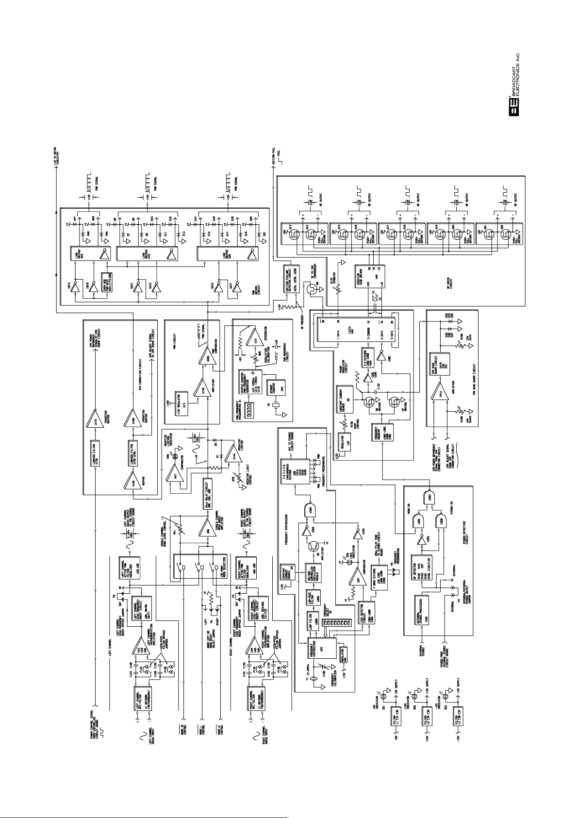
597-1112-24A
SIMPLIFIED SCHEMATIC
COPYRIGHT © 1997 BROADCAST ELECTRONICS, INC
(1-21/1-22)
FIGURE 1-2. EXCITER CIRCUIT BOARD
Page 87

1-118. LOCK DETECTOR CIRCUIT. The frequency synthesizer circuit is monitored for proper
operation by a lock detector circuit. Integrated circuits U28A, U28B, and U36A function
as a lock detector circuit. The circuit monitors an output sample signal and a divided
VCO sample signal from U25. If the VCO and the reference phases are within ±180
degrees, the VCO is locked to the correct frequency. If the phases are out of tolerance, the
output of U36A will go LOW. The LOW is applied to comparator U27. The output of U27
will go HIGH to extinguish lock indicator DS4 and is inverted at U33A. U33A will output
a LOW to U30B which mutes the output of the frequency synthesizer.
1-119. A sample from the lock detector circuit is applied to divide-by-3600 circuit. The circuit
consists of integrated circuits U34, U35A, U35B, U35C, and U36B. The divider circuit is
designed to generate a 25 Hz pilot signal for application to the stereo circuit board.
1-120.
1-121. Stereo signals from the stereo circuit board are applied to programmable jumper P7. P7
1-122. Either an external or internal stereo signal from P7 is applied to an RF detector circuit.
1-123. The mono/stereo select circuit will route a stereo or mono signal to an RF drive circuit in
1-124.
STEREO DETECTION CIRCUIT. The presence of a stereo signal is detected by a stereo
detection circuit. This circuit allows the transmitter to be: 1) converted to monophonic
operation by removing the stereo circuit board or 2) converted to stereophonic operation
by inserting the stereo circuit board. The circuit will also detect the presence of an
external stereo signal.
selects a stereo signal from the internal stereo circuit board or from an external source.
The external source is applied to a processing circuit consisting of integrated circuit U32C
and the associated circuitry. The processing circuit provides ac coupling, over-voltage
limiting, and square-wave generation.
The RF detector consists of: 1) resistors R151 through R155, 2) capacitors C124 and C125,
and 3) diode D27. The detector rectifies the signal for application to an automatic
mono/stereo select circuit consisting of integrated circuits U32A, U30B, U32C, and U32D.
response to the presence of stereo. If a stereo signal is present, the output of U32A will be
LOW. The LOW will disable mono on gate U30C and enable stereo on gate U32B. The
stereo signal from U32B will be applied through NAND gate U32D to a phase modulator
circuit. If a stereo signal is not present, the output of U32A will be HIGH. The HIGH
will enable U30C and disable U32B to allow the monophonic RF signal to be applied to the
phase modulator circuit.
IPM WAVE SHAPE CIRCUIT. The IPM adjust and IPM power reference signals from the
IPM correction circuit are applied to an IPM wave shape circuit. The signals are
amplified at U41A. The output of U41A is applied to an IPM wave shape circuit
consisting of integrated circuit U41B and diodes D30 and D31. The circuit is designed to
output a phase modulated signal which is equal in amplitude and out-of-phase with the
phase modulation component in the RF amplifier section. Potentiometer R198 controls
the shape of the IPM correction signal. Potentiometer R189 controls the amplitude of the
IPM correction signal. Diodes D32 through D37 provide over-voltage protection. The
output of the IPM wave shape circuit is applied to the phase modulator circuit.
1-125.
PHASE MODULATOR CIRCUIT. A phase modulator circuit is incorporated into the
exciter circuitry to cancel incidental-phase-modulation (IPM) in the RF amplifier section
of the transmitter. The circuit is designed to insert a phase modulation component which
is equal in amplitude and out of phase with the phase modulation in the RF amplifier
section. This feedforward approach is designed to effectively cancel (IPM) in the
transmitter.
1-25
Page 88

1-126. The phase modulator circuit accepts a mono or stereo signal from NAND gate U32D. The
signal is applied to a frequency doubler circuit consisting of integrated circuits U38A,
U38B, U38C, and U38D. The output of the frequency doubler is applied to the gates of
transistors Q6 and Q7. An IPM correction signal from the IPM wave shape circuit is
applied to the drains of Q6 and Q7.
1-127. Transistors Q6 and Q7 function to produce a triangle-shaped waveform which is equal in
amplitude and out-of-phase with the IPM in the RF amplifier section. The output from
Q6 and Q7 is converted to a square-wave at U33C and U33D. The signal from
U33C/U33D is applied to a divider circuit consisting of integrated circuits U39A, U39B,
and U33E. The output of the divider is used to clock the RF carrier signal from the
frequency doubler circuit at latch U40. U40 outputs a phase compensated carrier
frequency to the RF drive circuit. Potentiometer R170 is provided to adjust the symmetry
of the RF carrier signal.
1-128.
1-129.
1-130.
1-131.
1-132. EQUALIZATION CIRCUITRY. The stereo circuit board is equipped with two equalization
RF DRIVE CIRCUIT. The RF drive circuit consists of high/low side driver U46 and
transistors Q13 through Q22. Complementary phase compensated square-wave signals
at the carrier frequency are applied to U46. U46 outputs high and low driver signals for
application to a transistor array consisting of transistors Q13 through Q20. The
transistors output a +15 volt peak-to-peak square-wave signal at the carrier frequency
for application to the power block motherboard.
EXCITER FAILURE DETECTOR CIRCUIT. The exciter circuitry is equipped with an exciter
failure detector circuit. The circuit consists of integrated circuits U22B, U23A, and U23B.
Two signals are routed to the detector circuit: 1) the PWM control signal and 2) an RF
present signal from transistor Q8 and latch U40. The circuit is designed to output a
HIGH during the following conditions: 1) the loss of the PWM signal or 2) the loss of the
RF signal. The HIGH is routed to the circuitry on the controller circuit board.
POWER SUPPLY CIRCUITS. The exciter circuit board operates from three power
supplies: 1) a +5 volt supply, 2) a +15 volt supply, and 3) a -15 volt supply. Each supply is
equipped with a filter network. The +5 volt supply filter consists of inductor L1 and
capacitors C31/C32. The output of the filter is applied to: 1) +5 volt indicator DS1 and 2)
the exciter circuit board components. The +15 volt supply filter consists of inductor L2
and capacitors C34/C35. The output of the filter is applied to: 1) +15 volt indicator DS2
and 2) the exciter circuit board components. The -15 volt supply filter consists of inductor
L3 and capacitors C36/C37. The output of the filter is applied to: 1) -15 volt indicator
DS3 and 2) the exciter circuit board components.
STEREO CIRCUIT BOARD.
circuits: 1) equalization circuit 1 and 2) equalization circuit 2 (refer to Figure 1-3). The
circuits are designed to provide equalization for two antenna patterns such as: 1) a day
pattern and 2) a night pattern. The equalization circuits are identical and contain
identical left and right channel circuitry. Therefore, only the left channel of equalization
circuit 1 will be discussed.
1-26
Page 89
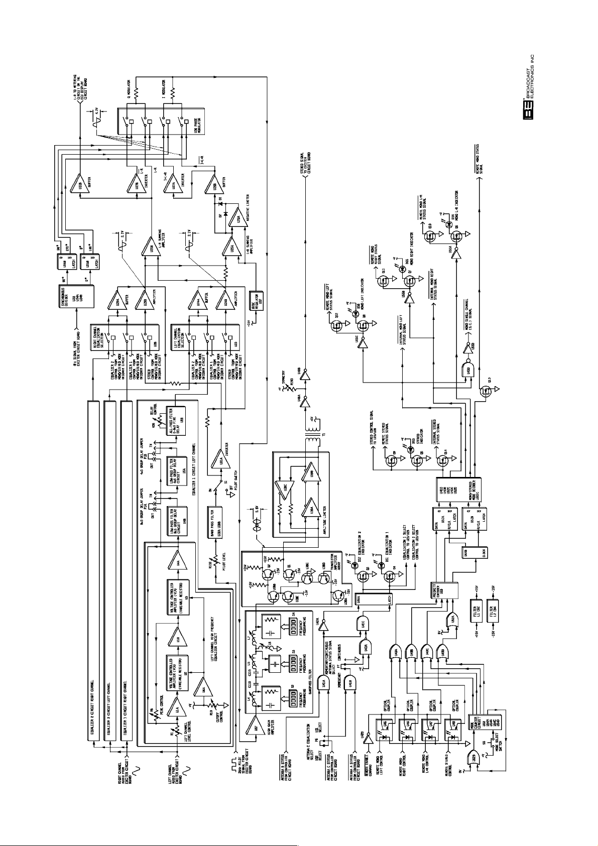
597-1112-25
SIMPLIFIED SCHEMATIC
COPYRIGHT © 1997 BROADCAST ELECTRONICS, INC
(1-27/1-28)
FIGURE 1-3. STEREO CIRCUIT BOARD
Page 90

1-133. Left channel audio from the exciter circuit board is applied to a left channel high
frequency equalizer network in the equalization 1 circuit. The high frequency equalizer
consists integrated circuits U1A, U2, U1B, U3, U4A, and U6A. The equalizer circuit is a
second order state variable low-pass filter designed to compensate for high frequency and
phase problems caused by antenna/phasor units. The filter is equipped with an
adjustable corner frequency. The corner frequency is established by a voltage generated
by potentiometer R20 and buffer U6A. The voltage is applied to
voltage-controlled-amplifiers U2 and U3 which control the corner frequency of the
equalizer circuit. In addition to the variable corner frequency, the filter is equipped with a
variable peak level. Potentiometer R6 controls the signal peak near the corner frequency.
Potentiometer R1 controls the left channel level. The output of the circuit is applied to an
8 microsecond delay circuit.
1-134.
1-135.
1-136.
1-137.
8 MICROSECOND DELAY CIRCUIT. Integrated circuit U4B is configured as an 8
microsecond delay circuit. The delay circuit is a third order low-pass filter designed to
provide 8 microseconds of delay to match low and mid frequency delay equalization
requirements. The output of the circuit is routed to 8 microsecond delay select jumper
P1A. P1A allows the delay circuit to be bypassed if 8 microseconds of delay is not
required for equalization operation.
4 MICROSECOND DELAY CIRCUIT. Integrated circuit U5A is configured as a 4
microsecond delay circuit. The delay circuit is a third order low-pass filter designed to
provide 4 microseconds of delay to match low and mid frequency delay equalization
requirements. The output of the circuit is routed to 4 microsecond delay select jumper
J1B. J1B allows the delay circuit to be bypassed if 4 microseconds of delay is not required
for equalization operation.
ALL-PASS FILTER. Integrated circuit U5B is configured as an all-pass filter circuit. The
circuit is designed to provide a continuously adjustable 0-6 microsecond delay for
equalization operation. Potentiometer R26 controls the amount of delay.
EQUALIZATION SELECTION CIRCUIT. The outputs of equalization circuits 1 and 2 are
applied to an equalization selection circuit consisting of integrated circuits U23 and U28.
U23 and U28 are single-pole switch arrays designed to select audio from the equalization
1 or equalization 2 circuit. U23 and U28 are controlled by: 1) HIGH equalization 1 and
equalization 2 control signals from latch U44A and 2) a HIGH stereo signal from the
mono/stereo mode decoder circuit. The circuit is designed to select audio in response to
the antenna pattern and mode of operation. For example, stereo audio from equalization
circuit 1 is required. A HIGH from latch U44A will enable the equalization 1 switches in
U23 and U28. U23 and U28 respond by routing audio to an L+R and L-R matrix circuit.
1-138.
L+R AND L-R MATRIX CIRCUIT. Left and right channel audio from the equalization
selection circuit is applied to an L-R and L+R matrix circuit. The circuit consists of
integrated circuits U24A, U24B, U25A, U26A, U26B, U27A, U29A, U29B, U25B, U31B,
U27B, U27A, and U32. The circuit is designed to generate L+R and L-R audio for
application to a phase modulator circuit.
1-29
Page 91

1-139. To provide an example of circuit operation, stereo audio is required from equalization
circuit 1. Left channel audio from the equalization circuit 1 input of U23 is applied to
buffer U24A. Right channel audio from the equalization circuit 1 input of U28 is applied
to buffer U29A. U24A and U29A will output audio which is summed with a pilot signal
from pilot on/off switch S1. The audio/pilot signal is applied to the inputs of U23/U28.
With a HIGH from the stereo control line of mono/stereo mode decoder circuit: 1) U23 will
route the left channel audio/pilot signal to amplifier U24B and 2) U28 will route the right
channel audio/pilot signal to amplifier U29B. U24B/U29B amplify the signal to
approximately 2.1 volts peak-to-peak. The outputs of U24B/U29B are applied to L+R
summing amplifier U25A and L-R summing amplifier U25B.
1-140. A dc voltage for application to L+R summing amplifier U25A is provided by regulator
U32. U32 provides a bias voltage for the L+R audio to generate a 1+L+R audio signal.
The output of summing amplifier U25A is applied to a negative limiter circuit consisting
of integrated circuit U26A and diodes D1 and D2. The circuit is designed to limit negative
modulation to -95%. This prevents the loss of carrier during negative modulation. The
output of negative limiter U26A is routed through buffer U26B to a phase modulator
circuit as a
application to a phase modulator circuit.
1-141. Left and right channel are summed at U25B to produce an L-R signal. The L-R signal is
applied to: 1) a phase modulator circuit as an L-R signal, 2) to inverter U27B, and
3) buffer U31B. U27B generates a
circuit. U31B is designed to buffer the L-R signal for application to an L-R metering
circuit on the ECU display circuit board.
1+L+R
signal and inverter U27B. U27B generates a 1+L+R signal for
signal for application to a phase modulator
L-R
1-142.
1-143. The phase modulator circuit operates from four phase references generated by a
1-144. Integrated circuit U36 is a switch array configured as a phase modulator. The four
1-145. The quadrature AM signal is applied to integrated circuit U37. U37 is a high-speed
PHASE MODULATOR CIRCUIT. 1+L+R,
phase modulator circuit. The phase modulator circuit consists of: 1) phase modulator
U36, 2) a synchronous divider consisting of integrated circuits U33, U34A, and U34B, and
3) latches U35A and U35B.
synchronous divider and latches U35A/U35B. A reference at four times the carrier
frequency from the exciter circuit board is applied to a synchronous divider circuit. The
circuit divides the signal by four and generates two outputs which are 90 degrees
out-of-phase. The outputs are applied to latches U35A/U35B. U35A/U35B generate four
reference signals: 1) 0 degrees, 2) 90 degrees, 3) 180 degrees, and 4) 270 degrees. The
reference signals are used to drive phase modulator U36.
reference signals from latches U35A/U35B are used to drive the 1+L+R,
and
modulated signal reference to a 0 degree carrier containing the L+R information (I
modulator) and 2) a double side-band suppressed carrier signal referenced to a 90 degree
carrier containing the L-R information (Q modulator). The signals are summed to
produce a quadrature AM signal.
operational amplifier designed to amplify the quadrature signal to a 1 volt peak-to-peak
level with no modulation. The output of the amplifier is applied to a band-pass filter.
signals at U36. The output of U36 produces two signals: 1) a normal AM
L-R
1+L+R
, L-R, and
signals are applied to a
L-R
1+L+R
, L-R,
1-30
Page 92

1-146. BAND-PASS FILTER. The output of amplifier U37 is applied to a forth order linear phase
band-pass filter. The band-pass filter consists of: 1) inductors L4, L5, L6, and L7,
2) capacitors C110 and C115, and 3) programming switches S2, S3, and S4. The filter
provides proper amplitude limiting during high single channel conditions. Programming
switches S2, S3, and S4 select resistor and capacitor combinations to program the filter
for specific groups of frequencies within the AM broadcast band. Inductors L4, L5, L6,
and L7 tune the filter for proper operation. The output of the filter is applied to a
transistor amplifier array.
1-147.
1-148.
1-149.
1-150.
TRANSISTOR AMPLIFIER CIRCUIT. The output of the band-pass filter is applied to a
transistor array consisting of transistors Q1, Q2, U38B, U38C, U38D, and U38E. The
signal is amplified to a 2 volt peak-to-peak level by transistors U38B, U38C, U38D, and
U38E. The transistors also perform unbalanced-to-balanced signal conversion. The
balanced signal from transistors U38B, U38C, U38D, and U38E are buffered by
transistors Q1 and Q2 for application to the amplitude limiter circuit.
AMPLITUDE LIMITER CIRCUIT. The balanced quadrature signal from the transistor
amplifier circuit is applied to an amplitude limiter circuit. The amplitude limiter circuit
consists of integrated circuits U39A, U39B, and U39C. The circuit produces phase
modulation containing the L-R information. The output of the limiter is applied to an
output network.
OUTPUT NETWORK. The 1 volt peak-to-peak phase modulated signal from the amplitude
limiter circuit is applied to transformer T1. T1 is provided to increase the
voltage to a 5 volt peak-to-peak level. The output of T1 is buffered by inverters U40A
and U40B. Potentiometer R193 adjusts the symmetry of the signal to null the second
harmonic frequency. The output of U40B is routed for application to the exciter circuit
board.
OPERATING MODE SELECTION AND INDICATION CIRCUIT. The stereo circuit board
can be configured for stereo, mono left, mono right, or mono L+R operation. The circuit
board is configured for the desired mode of operation by a mode selection and indication
circuit. HIGH remote mono left, mono right, mono L+R, and stereo commands are
applied to optical couplers U45 through U48. The outputs of U45 through U48 are
applied to OR gates U49A through U49D.
1-151. Local control operations are directed by mode select switch S5. S5 controls a mode
counter circuit consisting of integrated circuits U53, U54A, U54B, U54C, and U54D. The
switch operates by advancing the counter each time the switch is depressed. This results
in the circuit advancing through the modes of operation in the following order: 1) stereo,
2) mono left, 3) mono right, or 4) mono L+R. The mode counter circuit selects a mode by
routing a HIGH control command to the OR gates U49A through U49D.
1-152. OR gates U49A through U49D select a command from the remote control optical couplers
or the local mode counter circuit. For example, the circuit board is desired to be
configured for stereo operation. A HIGH from remote stereo optical coupler U48 or the
local mode control circuit is applied to OR gate U49D. U49D outputs a HIGH through OR
gate U52A to priority encoder U50. U50 monitors the OR gates for additional commands
and determines the highest priority mode of operation. Once the mode of operation is
determined, U50 will output a two bit binary code to a mono/stereo decoder circuit.
1-31
Page 93

1-153. The mono/stereo mode decoder circuit consists of: 1) latches U44B, U51A, and U51B and
2) mono/stereo decoder logic U41D, U43B, U43C, U52C, and U52D. Latches U51A and
U51B latch the two bit binary code and produce complementary outputs for application to
the mono/stereo decoder logic. Latch U44B operates as a clock for U51A/U51B. The
mono/stereo decoder logic decodes the binary code and outputs a HIGH to: 1) transistors
Q5, Q9, and Q14 and 2) equalization select integrated circuits U23 and U28. Transistor
Q14 will respond by generating a LOW internal stereo status signal. Transistor Q5 will
output a LOW to bias stereo indicator DS3 to on. Transistor Q9 will respond by
generating a LOW remote stereo status signal.
1-154. Selection and indication of the mono left, mono right, and mono L+R modes of operation
are performed in an identical manner. When the mono left or mono right mode is
selected, a HIGH will be routed to NAND gate U43D. The output of U43D will go HIGH.
The HIGH is inverted at U55D to produce a LOW mono single channel signal for
application to the exciter circuit board. When the mono left, mono right, or mono L+R
mode is selected a HIGH is applied to transistor Q13. Q13 will respond by generating a
LOW remote mono status signal.
1-155.
1-156. Antenna A, B, and C status signals are applied to AND gates U41A and U41B.
1-157. The circuit selects equalization circuit 1 or 2 when a status signal is applied to
1-158.
1-159. The output of the band-pass filter is applied through switch S1 to: 1) integrated circuit
EQUALIZATION SELECTION. Equalization circuit selection is determined by the antenna
connected to the transmitter. Antenna A selects equalization circuit 1. Antenna B selects
equalization circuit 2. Antenna C can be programmed to select equalization circuit 1 or
equalization circuit 2.
Programmable jumper P6 selects equalization circuit 1 or equalization circuit 2 for
antenna C operations.
U41A/U41B. For example, a LOW is applied to U41B when antenna A is selected. U41B
will output a LOW to NAND gate U43A. Programmable jumper P7 programs the
equalization selection circuit for momentary or continuous signals. With P7 programmed
for momentary signals, U43A will output a HIGH to AND gate U41C. With a HIGH from
U41A, U41C will output a HIGH to latch U44A. U44A will output a HIGH to:
1) integrated circuits U23 and U28 to select equalization circuit 1 and 2) transistor Q4.
Q4 will go LOW to bias equalization 1 indicator DS1 on.
PILOT SIGNAL. A 25 Hz square-wave signal from the exciter circuit board is applied
through potentiometer R132 to a band-pass filter consisting of integrated circuits U30A
and U30B. Potentiometer R132 is designed to provide pilot level control. The band-pass
filter converts the square-wave signal to a sine-wave signal.
U23 and 2) inverter U31A. U31A inverts the signal for application to integrated circuit
U28. Switch S1 is provided to disable the pilot signal.
1-160.
1-161.
1-162. The ECU assembly is equipped with a modular 40W switching power supply assembly.
POWER SUPPLY FILTER NETWORK. The stereo circuit board operates from ±15 volt
power supplies. Each supply is equipped with a filter network. The +15 volt supply filter
consists of inductor L1 and capacitor C92. The output of the filter is applied to the stereo
circuit board components. The -15 volt supply filter consists of inductor L2 and capacitor
C94. The output of the filter is applied to the stereo circuit board components.
ECU POWER SUPPLY ASSEMBLY.
The supply provides regulated +5V, +15V, and -15V operating potentials for the ECU
circuit boards.
1-32
Page 94

1-163. The power supply for the ECU controller circuit board is back-up by a 9V battery. During
an ac power failure, the battery will maintain the transmitter operating configuration
stored in the controller logic circuitry. Once power is returned to the transmitter, the
transmitter will automatically resume operation in the configuration appearing prior to
the ac failure. If an extended ac power failure occurs, the transmitter will be operated to
off by an ac loss/auto shutdown circuit on the controller circuit board.
1-33
Page 95

SECTION II
TRANSMITTER ECU MAINTENANCE
2-1. INTRODUCTION.
2-2. This section provides maintenance information for the AM-10A/AM-6A transmitter ECU
(exciter/control unit).
2-3.
SAFETY CONSIDERATIONS.
WARNING
THE TRANSMITTER CONTAINS MULTIPLE CIRCUIT
GROUNDS WITH HIGH AC AND DC POTENTIALS
WARNING
WARNING
WARNING
WITH RESPECT TO THE CABINET WHICH IS AT
EARTH POTENTIAL. DO NOT ENERGIZE THE
TRANSMITTER WITH TEST EQUIPMENT CONĆ
NECTED TO THE TRANSMITTER OUTPUT
NETWORK, RF POWER MODULE, RF COMBINER, OR
POWER SUPPLY COMPONENTS.
2-4. The AM-10A/AM-6A transmitters contain high voltages and currents. If safety
precautions are not practiced, contact with the high voltages and currents could cause
serious injury or death. The transmitter is equipped with many built-in safety features,
however good judgement, care, and common sense must be practiced to prevent accidents.
2-5. In addition to high voltages and currents, the transmitters contain multiple circuit
grounds with high ac and dc potentials with respect to the cabinet which is at earth
potential. The potentials could cause serious injury or death if maintenance personnel
simultaneously touch a circuit ground and the cabinet. As a result, operation of the
transmitter with test equipment connected to transmitter output network, RF power
module, RF combiner, or power supply components is extremely dangerous and must not
be attempted. Therefore, never energize the transmitter with test equipment connected
to the transmitter output network, RF power module, RF combiner, or power supply
components. Test equipment may be connected to the ECU circuit boards from the front
of the transmitter using the supplied extender circuit board with power energized. The
maintenance procedures presented in this section should be performed only by trained
and experienced maintenance personnel.
2-6.
2-7. The transmitter ECU is equipped with three circuit boards: 1) exciter, 2) stereo, and
ECU CIRCUIT BOARD INSTALLATION/REMOVAL.
3) controller. Each circuit board is equipped with finger holes for the ease of removal and
installation. To remove a circuit board, grasp the board using the finger holes and firmly
pull the circuit board out of the ECU.
2-1
WARNING: DISCONNECT POWER PRIOR TO SERVICING
Page 96

CAUTION
THE TRANSMITTER MAY BE DAMAGED IF THE ECU
CIRCUIT BOARDS ARE NOT SECURELY SEATED INTO
CAUTION
2-8. To install the circuit boards: 1) the boards must be inserted into the proper location in the
ECU and 2) the boards must be firmly seated into the ECU motherboard. To install a
circuit board, proceed as follows:
1. Refer to Figure 5-4 in PART I, SECTION V MAINTENANCE to determine the
circuit board location.
2. Insert the circuit board in the appropriate location.
3. Firmly press the circuit board into the connector to engage the connector
housing.
4. Firmly press the circuit board into the connector again to engage the
connector pins.
5. Repeat the procedure for each ECU circuit board.
THE CONNECTORS.
2-9.
2-10. First level maintenance consists of precautionary procedures applied to the equipment to
2-11.
FIRST LEVEL MAINTENANCE.
prevent future failures. The procedures are performed on a regular basis and the results
recorded in a performance log.
CLEANING AND INSPECTION.
WARNING
NEVER OPEN THE EQUIPMENT UNLESS ALL TRANSĆ
MITTER PRIMARY POWER IS DISCONNECTED. ENĆ
WARNING
SURE ALL TRANSMITTER PRIMARY POWER IS DISĆ
CONNECTED BEFORE ATTEMPTING MAINTENANCE
ON ANY AREA WITHIN THE TRANSMITTER.
2-12. Clean the ECU circuit boards of accumulated dust as required using a nylon bristle brush
and vacuum cleaner. Inspect the circuit boards for improperly seated semiconductors and
components damage by overheating. In addition, inspect the ECU for loose hardware.
Ensure all ECU interconnecting cables are secure.
2-13.
2-14. Second level maintenance is the performance of procedures required to restore the ECU to
2-15.
SECOND LEVEL MAINTENANCE.
operation after a fault has occurred. The procedures are divided into electrical
adjustments procedures and troubleshooting.
ELECTRICAL ADJUSTMENTS.
2-16. The following text provides electrical adjustment procedures for the transmitter ECU.
The procedures are presented in the following order.
1. ECU Extender Circuit Board Operation.
2. Controller Circuit Board Adjustments.
3. ECU Meter Switch Circuit Board Adjustments.
2-2
WARNING: DISCONNECT POWER PRIOR TO SERVICING
Page 97

4. Stereo Circuit Board Adjustments.
5. Exciter Circuit Board Adjustments.
6. Display Circuit Board Adjustments.
2-17.
2-18. The ECU is equipped with an extender circuit board. The circuit board is designed to
2-19.
2-20. P1 SET - P5 SET CONTROLS. The P1 SET through P5 SET controls adjust the ECU
ECU EXTENDER CIRCUIT BOARD OPERATION.
allow access to the ECU circuit board components for maintenance procedures. To use the
circuit board for maintenance procedures, proceed as follows:
1. Refer to Figure 5-4 in PART I, SECTION V MAINTENANCE and locate the
extender circuit board assembly in the ECU.
2. Remove the extender circuit board from the ECU.
3. Loosen the extender circuit board locking nut.
4. Completely extend the circuit board.
5. Tighten the extender circuit board locking nut.
6. Remove the circuit board required for maintenance and place the extender
circuit board in the location in the ECU.
7. Place the desired circuit board onto the extender circuit board.
8. Firmly press the circuit board into the extender circuit board connectors.
CONTROLLER CIRCUIT BOARD ADJUSTMENTS.
POWER CONTROL 1 through 5 controls to desired levels. A complete description of the
procedure to adjust the power level controls is presented in SECTION II,
INSTALLATION. Refer to POWER LEVEL AND MODULATION CALIBRATION
ADJUSTMENT in SECTION II for the adjustment procedure.
2-21.
2-22.
2-23. FORWARD POWER METER LOW AND HIGH SCALE CALIBRATIONS. Low scale
2-24.
FWD AND RFL CALIBRATIONS. FWD CAL control R56 and RFL CAL control R143
calibrate the transmitter forward and reflected power samples. Due to the critical nature
of the FWD CAL and RFL CAL controls, the controls are not considered field adjustable.
If the controls are required to be adjusted, contact the Broadcast Electronics Customer
Service Department for information and instructions to adjust the FWD and RFL CAL
controls.
ECU METER SWITCH CIRCUIT BOARD ADJUSTMENTS.
control R501 and high scale control R504 calibrate the forward power meter. Due to the
critical nature of the low scale and high scale meter calibrate controls, the controls are not
considered field adjustable. If the controls are required to be adjusted, contact the
Broadcast Electronics Customer Service Department for information and instructions to
adjust the low and high scale forward power meter controls.
REFLECTED POWER METER LOW AND HIGH SCALE CALIBRATIONS. Low scale
control R505, high scale control R506, and ac sample control R511 calibrate the reflected
power meter. Due to the critical nature of the low scale, high scale, and ac sample meter
calibrate controls, the controls are not considered field adjustable. If the controls are
required to be adjusted, contact the Broadcast Electronics Customer Service Department
for information and instructions to adjust the low scale, high scale, and ac sample
reflected power meter controls.
2-3
WARNING: DISCONNECT POWER PRIOR TO SERVICING
Page 98

2-25. FWD AND RFL CALIBRATIONS. FWD CAL control R56 and RFL CAL control R143
calibrate the transmitter forward and reflected power samples. Due to the critical nature
of the FWD CAL and RFL CAL controls, the controls are not considered field adjustable.
If the controls are required to be adjusted, contact the Broadcast Electronics Customer
Service Department for information and instructions to adjust the FWD and RFL CAL
controls.
STEREO CIRCUIT BOARD ADJUSTMENTS.
2-26.
2-27. STEREO ADJUSTMENT. The stereo adjustment consists of configuring the equalization
circuitry on the stereo circuit board to obtain the optimum stereo performance. The
equalization circuitry consists of the equalization circuit 1 and equalization circuit 2
controls. A complete description of the procedure to adjust the equalization controls is
presented in SECTION II, INSTALLATION. Refer to STEREO ADJUSTMENT in
SECTION II for the adjustment procedure.
2-28.
2-29. MODULATION CALIBRATION. Modulation calibration control R62 calibrates the exciter
2-30.
2-31.
2-32.
2-33.
2-34.
2-35.
EXCITER CIRCUIT BOARD ADJUSTMENTS.
modulation circuit. Due to the critical nature of the modulation calibration control, the
control is not considered field adjustable. If the control is to be adjusted, contact the
Broadcast Electronics Customer Service Department for information and instructions to
adjust the modulation calibration control.
PHASE MODULATOR CALIBRATION. Phase modulator calibration control R159
calibrates the exciter phase modulator circuit. Due to the critical nature of the phase
modulator calibration control, the control is not considered field adjustable. If the control
is to be adjusted, contact the Broadcast Electronics Customer Service Department for
information and instructions to adjust the phase modulator calibration control.
SYMMETRY CONTROL. Symmetry calibration control R170 adjusts the exciter RF
output square-wave signal. Due to the critical nature of the symmetry control, the
control is not considered field adjustable. If the control is to be adjusted, contact the
Broadcast Electronics Customer Service Department for information and instructions to
adjust the symmetry control.
IPM CORRECTION CIRCUIT CONTROLS. IPM GAIN control R189, IPM TRACK control
R104, IPM SHAPE CONTROL R198, and IPM ZERO SET control R191 calibrate the IPM
correction circuit. Due to the critical nature of the IPM correction circuit controls, the
controls are not considered field adjustable. If the controls are to be adjusted, contact the
Broadcast Electronics Customer Service Department for information and instructions to
adjust the IPM correction circuit controls.
SINGLE CHAN MONO LEVEL CONTROL. SINGLE CHAN MONO LEVEL control R41
is designed to boost a remaining audio channel level in the event of a failure in one
channel. A complete description of the procedure to adjust the SINGLE CHAN MONO
LEVEL control is presented in SECTION II, INSTALLATION. Refer to SINGLE
CHANNEL LEVEL in SECTION II for the adjustment procedure.
AVERAGE MODULATION LIMIT CONTROL. Average modulation limit control R217
limits the average tone modulation. The control is adjusted to limit at 110% tone
modulation. Due to the critical nature of the modulation calibration control, the control is
not considered field adjustable. If the control is to be adjusted, contact the Broadcast
Electronics Customer Service Department for information and instructions to adjust the
average modulation limit control.
NEG LIMIT CONTROL. NEG LIMIT control R76 limits the negative L+R information to
prevent excessive modulation when the L+R signal is summed with the pilot tone. The
NEG LIMIT control is adjusted in the following procedure.
2-4
WARNING: DISCONNECT POWER PRIOR TO SERVICING
Page 99

2-36. Procedure. To adjust NEG LIMIT control R76, proceed as follows:
WARNING
DISCONNECT ALL TRANSMITTER PRIMARY POWER
BEFORE PROCEEDING.
WARNING
2-37. Disconnect all transmitter primary power.
2-38. Connect the audio generator to the TB2 LEFT INPUT and RIGHT INPUT audio
terminals on the ECU rear-panel.
2-39. Adjust NEG LIMIT control R76 on the exciter circuit board fully counterclockwise.
2-40. Adjust the audio generator for a L=R 1 kHz output at +10 dBm.
2-41. Adjust the AM stereo modulation monitor to indicate positive L+R modulation.
2-42. Energize the transmitter primary power and operate the transmitter.
2-43. Observe the modulation monitor and ensure the monitor indicates 100% positive L+R
modulation. If the monitor does not indicate 100% L+R modulation, adjust the audio
generator level slightly for a +100% L+R modulation indication on the monitor.
2-44. Adjust the AM stereo modulation monitor to indicate negative L+R modulation.
2-45. Adjust NEG LIMIT control R76 on the exciter circuit board until the AM stereo
Modulation monitor indicates -95% L+R modulation.
WARNING
DISCONNECT ALL TRANSMITTER PRIMARY POWER
BEFORE PROCEEDING.
WARNING
2-46. Disconnect all transmitter primary power.
2-47. Remove all test equipment.
2-48.
2-49. Procedure. To adjust frequency calibration control C108, proceed as follows:
FREQUENCY CALIBRATION CONTROL. Frequency calibration control C108 calibrates
the exciter frequency synthesizer. The frequency calibration control is adjusted in the
following procedure.
WARNING
DISCONNECT ALL TRANSMITTER PRIMARY POWER
BEFORE PROCEEDING.
WARNING
2-50. Disconnect all transmitter primary power.
2-51. Remove the exciter circuit board and install the ECU extender circuit board in the exciter
circuit board location.
2-52. Install the exciter circuit board on the extender circuit board.
2-53. Connect a frequency counter to test point TP15 on the exciter circuit board.
2-54. Energize the transmitter primary power and operate the transmitter.
2-55. Adjust frequency calibration control C108 on the exciter circuit board for to the carrier
frequency.
2-5
WARNING: DISCONNECT POWER PRIOR TO SERVICING
Page 100
WARNING
DISCONNECT ALL TRANSMITTER PRIMARY POWER
BEFORE PROCEEDING.
WARNING
2-56. Disconnect all transmitter primary power.
2-57. Remove all test equipment and replace the exciter circuit board.
2-58.
2-59. L/L+R AND R/L-R DISPLAY CALIBRATION CONTROL. L/L+R calibration control R42
2-60. Procedure. To adjust L/L+R calibration control R42 and R/L-R calibration control R48,
DISPLAY CIRCUIT BOARD ADJUSTMENTS.
and R/L-R calibration control R48 calibrate the L/L+R and R/L-R displays. The L/L+R
and R/L-R calibration controls are adjusted in the following procedure.
proceed as follows:
WARNING
DISCONNECT ALL TRANSMITTER PRIMARY POWER
BEFORE PROCEEDING.
WARNING
2-61. Disconnect all transmitter primary power.
2-62. Connect the audio generator to the TB2 LEFT INPUT and RIGHT INPUT audio
terminals on the ECU rear-panel. Operate the transmitter at a normal output power and
the EXCITER MONITOR for L+R/L-R indications.
2-63. Adjust the audio generator for an in-phase L=R 1 kHz output at a level to generate 100%
modulation as indicated by the modulation monitor. Adjust L/L+R calibration control R42
until the EXCITER MONITOR just indicates 100% L+R modulation.
2-64. Adjust the audio generator for an out-of-phase L=R 1 kHz output at a level to generate
100% L-R modulation as indicated by the modulation monitor. Adjust R/L-R calibration
control R48 until the EXCITER MONITOR just indicates 100% L-R modulation.
WARNING
DISCONNECT ALL TRANSMITTER PRIMARY POWER
BEFORE PROCEEDING.
WARNING
2-65. Disconnect all transmitter primary power and remove all test equipment.
2-66.
TROUBLESHOOTING.
WARNING
THE TRANSMITTER CONTAINS MULTIPLE CIRCUIT
GROUNDS WITH HIGH AC AND DC POTENTIALS
WARNING
WARNING
WARNING
WITH RESPECT TO THE CABINET WHICH IS AT
EARTH POTENTIAL. DO NOT ENERGIZE THE
TRANSMITTER WITH TEST EQUIPMENT CONĆ
NECTED TO THE TRANSMITTER OUTPUT
NETWORK, RF POWER MODULE, RF COMBINER, OR
POWER SUPPLY COMPONENTS.
2-67. SAFETY CONSIDERATIONS. The AM-10A/AM-6A transmitters are equipped with
extensive indicator and meter circuitry to allow the operator to isolate problems to a
specific area within the transmitter. Due to the hazardous voltages and currents
contained in the equipment, operation of the transmitter with test equipment connected
to transmitter output network, RF power module, RF combiner, or power supply
components is extremely dangerous and must not be attempted. Test equipment may be
connected to the ECU circuit boards from the front of the transmitter using the supplied
extender circuit board with power energized. Therefore, the transmitter indicators and
meters must be used to isolate a problem to a specific area. The maintenance procedures
presented in this section should be performed only by trained and experienced
maintenance personnel.
2-6
WARNING: DISCONNECT POWER PRIOR TO SERVICING
 Loading...