

Page 1

ATB Reference
ANALOG
TERMINAL
BOARD
MANUAL
2.01 EDITION
AUGUST 1997
Intro-1
Page 2

ATB Reference
Thank You For Buying
The Analog Terminal
Board!
We proudly present the Analog Terminal Board.
The Analog Terminal Board is the easiest and tidiest way of
connecting real world devices to our range of AD1200 Analog to
Digital acquisition systems.
Your board is designed and manufactured in England, and
our policy is one of complete support to our dealers and direct
to our users. Do not hesitate to contact us, on our HOTLINE
numbers given on Intro page 2, if you need help.
We trust that you will enjoy many years of useful service
from your Analog Terminal Board.
ATB MANUAL______________
The Layout Of This Manual._________________________
This manual is a complete description of how to install and
use the Analog Terminal Board for AD1200 interface cards.
Chapter 1, Analog Terminal Board, describes the
use and features of the analog terminal board, it has a host of
many handy features.
Intro-3
Page 3

ATB Reference
Contents._________
Introduction. 1
The Analog Screw Terminal Board 1
Fused Power Rails. 2
Attaching The Optional LED’s. 2
Jumpers Settings, W1-W4. 3
Differential Analog Inputs, 8DI. 3
4-20mA Current Inputs. 4
Thermocouple Cold Junction Compensation. 5
List Of Figures.
Figure 1-1. Optional LEDs 3
Figure 1-2. Jumper Table. 3
Figure 1-3. Resistor Table, DI Inputs. 6
Figure 1-4. Resistor Table, SE Inputs. 6
Figure 1-5. ATB J1 Pin Outs. 7
Intro-4
Page 4

Analog Terminal Board Reference
ANALOG SCREW
TERMINAL BOARD.
Introduction.____________
This manual explains the functions and features of the
Analog Screw Terminal Board. Apart from bringing the AD1200
cards i/o lines out to easily accessible terminals the Analog
Terminal Board is designed to take several user fitted
components. Which components are fitted is determined by the
users application and by how the AD1200 card has been
configured.
The user applications covered include voltage, current and
thermocouple inputs. Whilst the ATB has features to deal with
the AD1200 card configured for 16 Single Ended, 8 Differential
Input or 16 Pseudo Differential Input channels.
Details are given on how to configure the card to deal with
all these options. Instructions of how to add the optional LEDs
and pullup resistors to the digital port lines are also included.
The Analog Screw Terminal Board _______________________________
The Analog Screw Terminal Board is the easiest and tidiest
way to connect PC AD1200 cards to the users own rig.
The Analog Screw Terminal Board converts from the 50
IDC ribbon cable to screw terminals, making all the AD1200
pinouts easily accessible. The screw terminals can take wire up
to 2.5mm, 0.1 inch, in diameter. The 50IDC entry is a latching
connector. The four plastic mounting feet may be removed and
the terminal board used as a screw mounted panel.
The ATB has been designed to provide the following
features:a) Clearly labelled, accessible port lines.
b) Provision for necessary DI return resistors.
c) Fuses for the +/-12 Volt lines.
d) Provision for user fitted 4-20mA current shunts in 8 DI
mode (and exceptionally in 16 SE mode).
Page 1
Page 5

Reference Analog Terminal Board
e) Provision for LED indication of TTL digital line levels.
f) Provision for cold junction compensation circuitry, CJC, for
thermocouple inputs. ATB-CJC version only!
Fused Power Rails._________________
The +12Volt and -12Volt power lines are lead via 62mA
fuses to the 2nd terminal of the Digital i/o port rails.
It is recommended that not more than 50 mA is drawn
from the PC! Earlier style PC’s may have a low wattage
power supply and therefore LESS power should be drawn
from these type of PC’s.
Attaching The Optional LED’s.___________________________
Each of the 16 digital i/o signal lines of the ATB can have
an optional LED and current limiting attached, this can be used
as an onboard indicator of the signal logic level. Depending on
the circuits connected to these lines it may not be appropriate to
have an LED and resistor attached so this is an optional, user
fitted feature. The current limiting resistor is nominally 470
Ohm, though anything in the range 100 Ohm to 1k Ohm will
work.
Figure 1-1. Optional LED._______________________
Attach the led’s and resistor
to required screw terminals.
Care should be taken to ensure
that the LED is connected the
correct way round, long leg is
the Anode, and that the ATB
is disconnected from both the
Only connect an LED if the current taken by the resistor and
LED will not effect the rest of the circuit to that terminal line.!
Page 2
PC and any user circuitry that
is powered up!
Page 6

Analog Terminal Board Reference
Jumpers Settings, W1-W4._______________________
There are four jumpers on the ATB. The functions are
summarised in Figure 1-2.
Jumpers W1 and W2 are used only in with the thermocouple
cold junction compensation circuitry. W1 connects the CH0 input
to the cold junction circuit whilst W2 connects the CH0 return
line to ANALOG ground.
Jumper W3 connects the system ground, SYS GND, to the
ANALOG ground. Single Ended inputs normally have a return
path via analog ground and this jumper connects the analog
ground to SYS GND.
Jumper W4 connects the AMPLOW to the ANALOG ground.
Pseudo differential inputs are referenced to AMPLOW. This
jumper can be used in conjunction to W3 to connect AMP LOW
to the system ground SYS GND.
Figure 1-2. Jumper Table._______________________
ЪДДДДДДДДДДДДДДДДДДДДДДДДДДДВДДДДДДДДДДДДДДДДДДДДДДДДДДДДДДДД¿
³
³
Jumper Settings
³
ГДДДДДДВДДДДДДВДДДДДДВДДДДДДЕДДДДДДДДДДДДДДДДДДДДДДДДДДДДДДДД´
³ý
W1
ГДДДДДДЕДДДДДДЕДДДДДДЕДДДДДДЕДДДДДДДДДДДДДДДДДДДДДДДДДДДДДДДД´
³ýý
ГДДДДДДЕДДДДДДЕДДДДДДЕДДДДДДЕДДДДДДДДДДДДДДДДДДДДДДДДДДДДДДДД´
³ýý
ГДДДДДДЕДДДДДДЕДДДДДДЕДДДДДДЕДДДДДДДДДДДДДДДДДДДДДДДДДДДДДДДД´
³ýý
³ýý
АДДДДДДБДДДДДДБДДДДДДБДДДДДДБДДДДДДДДДДДДДДДДДДДДДДДДДДДДДДДДЩ
In
ý³ýý
Out
ý³ýý
Out
ý³ýý
ýý³
³ý
W2
In
Out
Out
³ý
W3
ý³ýý
In
ý³ýý
In
ý³ýý
In
ýý³ý
³ý
W4 ³
ý³ýý
ý³ýý
ý³ýý
ý³
In
In
In
³
³
Input Types
³
ý³
Active Thermocouple CJC
ý³
4-20mA Current Inputs
ý³
Voltage Inputs
ý³ý
ýýý
³
³
³
³
³
³
³
³
Differential Analog Inputs, 8DI.____________________________
Always use the 8 Differential input scheme, in preference
to any other scheme, where ever possible and also when:a) using low level input signals, (less than 1 Volt full scale).
b) in noisy environments.
c) there is no common ground shared by the analog signal
sources.
The 10k Ohm Differential return path resistors should be fitted,
Page 3
Page 7

Reference Analog Terminal Board
these are 10k 1/4 watt nominal value, though anything in the
range 1k-100k would be adequate. Installing these resistors
causes the return side of each channel to be referenced to the
system ground, SYS GND. The return resistors for channels 0 to
7 are R14, R10, R6, R2, R15, R11, R7 and R3 respectively. See
Figure 1-3.
Figure 1-3. Resistor Table, DI Inputs.________________________________
ЪДДДДДДДДДДДДДДДДДДДДДДДДДДДДДДДДДДДДДДДДДДДДДДДДДДДДДДДДДДДДДДДДДДД¿
³ý
ГДДДДДДДДДДДДДДВДДДДДВДДДДДВДДДДДВДДДДДВДДДДДВДДДДДВДДДДДВДДДДДВДДДД´
³
³
Function
ГДДДДДДДДДДДДДДЕДДДДДЕДДДДДЕДДДДДЕДДДДДЕДДДДДЕДДДДДЕДДДДДЕДДДДДЕДДДД´
³ý
Thermocouple
³ý
Open Circuit
³ý
Detection
ГДДДДДДДДДДДДДДЕДДДДДЕДДДДДЕДДДДДЕДДДДДЕДДДДДЕДДДДДЕДДДДДЕДДДДДЕДДДД´
³ý
Differential
³ý
Return Path
³ý
To Analog Gnd
ГДДДДДДДДДДДДДДЕДДДДДЕДДДДДЕДДДДДЕДДДДДЕДДДДДЕДДДДДЕДДДДДЕДДДДДЕДДДД´
³ý
4-20mA
³ý
Current Shunt
³ý
(0-5V input)
³
АДДДДДДДДДДДДДДБДДДДДБДДДДДБДДДДДБДДДДДБДДДДДБДДДДДБДДДДДБДДДДДБДДДДЩ
*NOTE: R26 NOT REQUIRED WHEN CJC CIRCUITRY IS BEING USED.
ýýýý
Resistors 8 DI Differential Inputting
³
³ ³ ³ ³ ³ ³ ³ ³
³
0 ³ 1 ³ 2 ³ 3 ³ 4 ³ 5 ³ 6 ³ 7 ³Ohms
³
³ ³ ³ ³ ³ ³ ³ ³
³
R26 ³ R27 ³ R28 ³ R29 ³ R30 ³ R31 ³ R32 ³ R33 ³100M
³
*NOTE³ ³ ³ ³ ³ ³ ³ ³
³
³ ³ ³ ³ ³ ³ ³ ³
³
R14 ³ R10 ³ R6 ³ R2 ³ R15 ³ R11 ³ R7 ³ R3 ³10k
³
³ ³ ³ ³ ³ ³ ³ ³
³
³ ³ ³ ³ ³ ³ ³ ³
³
R13 ³ R9 ³ R5 ³ R1 ³ R16 ³ R12 ³ R8 ³ R4 ³250R
³
³ ³ ³ ³ ³ ³ ³ ³%tol
³
³ ³ ³ ³ ³ ³ ³ ³0.01
ý³
³
³
³
³
³
³
³
³
³
³
³
³
4-20mA Current Inputs._____________________
The 4-20mA current input scheme is commonly used in
industry. 4-20mA currents are inherently differential inputs since
current flow round a CIRCUIT there is the current terminal and
its return line, there the AD1200 card will be configured for 8
DI inputs. Currents can be sent a long way without degradation
(there is Law of Conservation of Current but no Law of
Conservation of Voltage) and are remarkably free of interference.
The AD1200 series have voltage inputs so the the 4-20mA
current inputs have to be turned into voltages for the A/D card
to be able to convert the signals. When a current passes through
a resistor a voltage is generated and this is the simple basis for
Page 4
Page 8
Analog Terminal Board Reference
turning the 4-20mA inputs into voltages. Set the A/D card for 8
channels differential input, Unipolar 0-5 Volt range. Install the
current shunt resistors. These should be high precision 250 Ohm
resistors, 0.01% or better. These give an output voltage of
250mV per mA. Thus 4mA gives 1 Volt input, 20mA gives 5
Volts input, 0 volts input is open circuit.
The current shunt resistors for channels 0 to 7 are R13, R9, R5,
R1, R16, R12, R8 and R4 respectively. See Figure 1-3. Only
resistors for the number of channels actually being used in this
mode need be fitted.
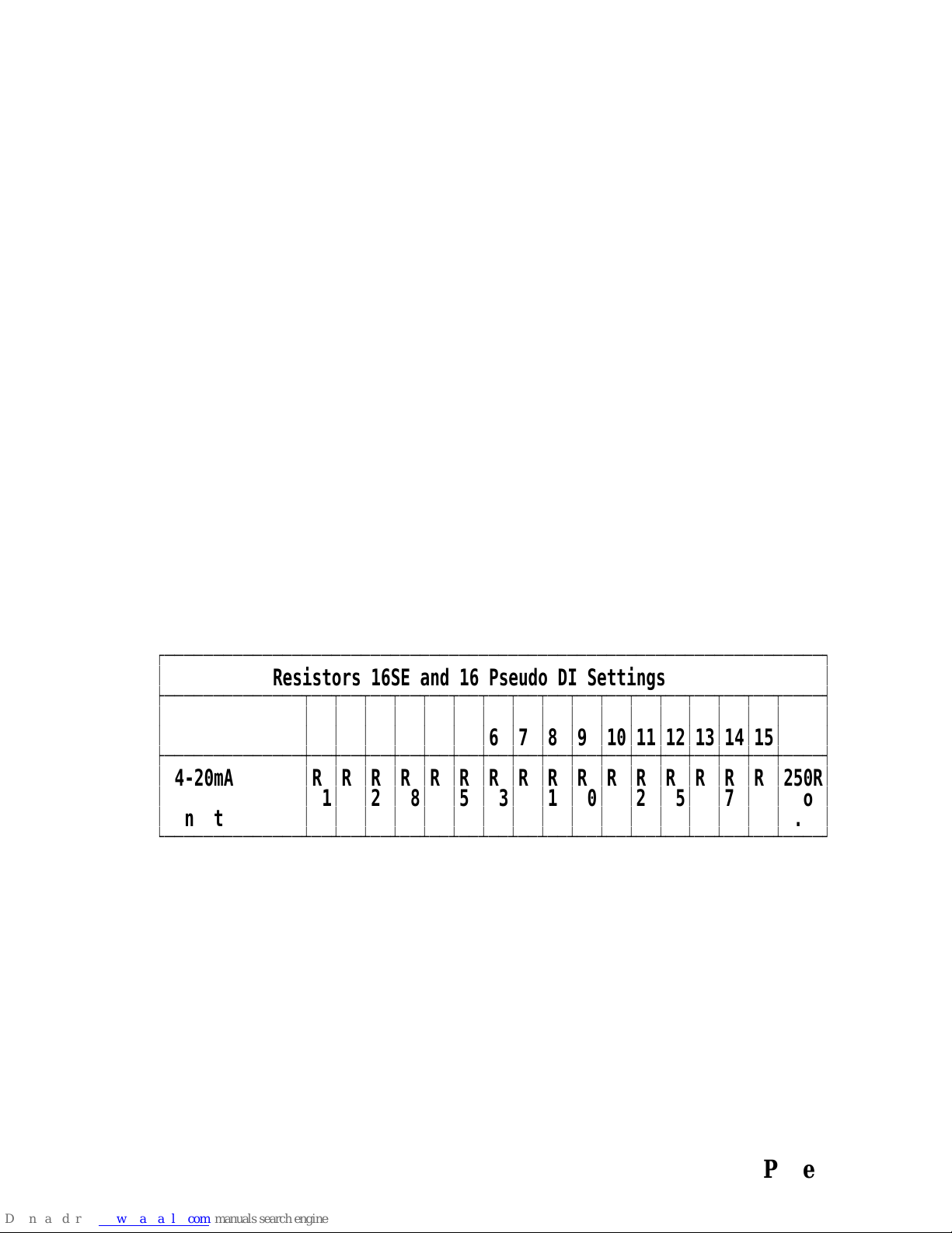
In exceptional circumstances 16 current inputs may be used,
when the AD1200 card is set to 16 SE or 16 Pseudo DI inputs.
In this case the resistors R14, R10, R6, R2, R15, R11, R7 and
R3 marked out as DI 10k return resistors and R18, R20 and
R50-55 should be fitted with the 250Ohm 0.01% tolerance
current shunts as shown in Figure 1-4.
Figure 1-4. Resistor Table, SE Inputs._________________________________
ЪДДДДДДДДДДДДДДДДДДДДДДДДДДДДДДДДДДДДДДДДДДДДДДДДДДДДДДДДДДДДДДДДДДД¿
³ý
ГДДДДДДДДДДДДДДВДДВДДВДДВДДВДДВДДВДДВДДВДДВДДВДДВДДВДДВДДВДДВДДВДДДД´
³
³
Function
ГДДДДДДДДДДДДДДЕДДЕДДЕДДЕДДЕДДЕДДЕДДЕДДЕДДЕДДЕДДЕДДЕДДЕДДЕДДЕДДЕДДДД´
³ý
4-20mA
³ý
Current
³ý
Inputs
АДДДДДДДДДДДДДДБДДБДДБДДБДДБДДБДДБДДБДДБДДБДДБДДБДДБДДБДДБДДБДДБДДДДЩ
ýýýý
Resistors 16SE and 16 Pseudo DI Settings
³ ³ ³ ³ ³ ³ ³ ³ ³ ³ ³ ³ ³ ³ ³ ³ ³
³0 ³1 ³2 ³3 ³4 ³5 ³6 ³7 ³8 ³9 ³10³11³12³13³14³15³
³R ³R ³R ³R ³R ³R ³R ³R ³R ³R ³R ³R ³R ³R ³R ³R ³
³51³50³25³18³55³54³53³52³14³10³6 ³2 ³15³11³7 ³3 ³
³ ³ ³ ³ ³ ³ ³ ³ ³ ³ ³ ³ ³ ³ ³ ³ ³
ý³
ý³
ý³
250R
³
%tol
³
0.01
³
Page 5
Page 9

Reference Analog Terminal Board
Thermocouple Cold Junction Compensation, CJC.____________________________________________
Much of the following information was gleaned from the
Analog Devices "Transducer Interfacing Handbook - A Guide to
Signal Conditioning." Edited by Daniel H. Sheingold ISBN 0916550-05-2, see especially Chapter 7 "Thermoswitches and
Thermocouples". This is a tremendously good reference book
about all sorts of signal acquistion and conditioning.
The circuitry to support thermocouples attached to the
AD1200 series boards consists of two parts:- the cold junction
compensation, CJC, circuitry and the open circuit detection for
each individual thermocouple attached. Thermocouples are
inherently differential, so the AD1200 card should be configured
for 8 differential inputs, DI, and so the 10k Ohm Differential
return path resistors should be fitted.
Open Circuit Detection.
Thermocouples are used to measure temperatures and are so
subject to heating and cooling stress, in addition they are usually
in HOT places and so not available for easy inspection. If a
break occurs in the thermocouple or its connecting lead it may
be difficult to tell. The open circuit detection is a simple but
effective method of telling that the thermocouple circuit has a
break somewhere. A large pull up resistor is attached to one end
of the thermocouple. The other end of the resistor is attached to
a bias voltage, VBIAS of 2.4 Volts. A break in the line causes
the A/D input to go to full scale. When a full scale input is read
by the computer, the user knows that the thermocouple
connection has broken.
Open circuit detection is sometimes known as up line break
detection.
Resistor R20, 10k and Zener diode ZD1 of 2.4Volts
connected between +12 and Analog ground generate the bias
voltage. Resistors R26, R27, R28, R29, R30, R31, R32 and R33,
one each for channels 0 to 7 respectively, are the 100 Meg Ohm
bias pull up resistors. See Figure 1-3. Only resistors for the
number of channels actually being used in this mode need be
Page 6
Page 10

Analog Terminal Board Reference
fitted.
Thermocouple Outputs.
A thermocouple is the junction between two dissimilar metals,
the TYPE of thermocouple depends on the metals used.
Thermocouples generate an output voltage that varies with
temperature, as observed initially by T. Seebeck in 1821. Thus
by accurately measuring the voltage generated by a thermocouple
the temperature is precisely known.
Unfortunately the relationship bewteen temperature and voltage is
not a linear one. IE the graph of temperature against voltage is
not a straight line. The situation is further complicated by the
fact that different types of thermocouples are needed to cover
different temperature ranges and each thermocouple types voltage
output has its own particular way of varying with temperature.
The best way of turning a thermocouple voltage into
temperature, and vice versa, is by using a printed table. Several
are in use. Two common sources of data are the American
National Standard C96.2 1973, published as ASTM document E
230-72 and "Temperature Sensing with Thermocouples and
Resistance Thermometers" by Labfacility Ltd available from
Farnell as order code 182-714 price £2.90. The different types of
thermocouple are known by various letters of the alphabet eg J,
K, R, S, T, B, and E etc. Figure 1-x is taken from ASTM
document E 230-72.
Page 7
Page 11

Reference Analog Terminal Board
Figure 1-5. Voltage as Function Of Temperature.__________________________________________
ЪДДДДДДДДДДДДВДДДДДДДДДДДДДДДДДДДВДДДДДДДДДДДДДДДДДДД¿
³ý
TEMP
³
degrees
³
Centigrade
³
ГДДДДДДДДДДДДЕДДДДДДДДЕДДДДДДДДДДЕДДДДДДДДЕДДДДДДДДДД´
³
-200
³
-100
³
0
³
25
³
100
³
200
³
300
³
400
³
500
³
600
³
700
³
800
³
900
³
1000
³
1100
³
1200
³
АДДДДДДДДДДДДБДДДДДДДДБДДДДДДДДДДБДДДДДДДДБДДДДДДДДДДЩ
³
J Type
ГДДДДДДДДВДДДДДДДДДДЕДДДДДДДДВДДДДДДДДДД´
³
Output ³ Tempco ³ Output ³ Tempco
³
mVolts ³ microV/C ³ mVolts ³ microV/C
³
-7.890 ³ 21.8 ³ -5.891 ³ 15.2
³
-4.632 ³ 41.1 ³ -3.553 ³ 30.5
³
0.000 ³ 50.4 ³ 0.000 ³ 39.5
³
1.277 ³ 51.7 ³ 1.000 ³ 40.5
³
5.268 ³ 54.4 ³ 4.095 ³ 41.4
³
10.777 ³ 55.5 ³ 8.137 ³ 39.9
³
16.325 ³ 55.4 ³ 12.207 ³ 41.5
³
21.846 ³ 55.2 ³ 16.395 ³ 41.9
³
27.388 ³ 55.9 ³ 20.640 ³ 42.6
³
33.096 ³ 58.5 ³ 24.902 ³ 42.5
³
39.130 ³ 62.3 ³ 29.128 ³ 41.9
³
45.498 ³ 64.6 ³ 33.277 ³ 41.0
³
51.875 ³ 62.4 ³ 37.325 ³ 39.9
³
57.942 ³ 59.2 ³ 41.269 ³ 38.9
³
63.777 ³ 57.8 ³ 45.108 ³ 37.8
³
69.536 ³ 57.2 ³ 48.828 ³ 36.5
³
³ ³ ³
³
K Type
ý³
³
³
³
³
³
³
³
³
³
³
³
³
³
³
³
³
³
³
³
Figure 1-6. Temperature as Function Of Voltage.__________________________________________
ЪДДДДДДДДДДДДВДДДДДДДДДДДДДДДДДДДВДДДДДДДДДДДДДДДДДДД¿
³ý
VOLTAGE
³
³
milliVolts
³
ГДДДДДДДДДДДДЕДДДДДДДДЕДДДДДДДДДДЕДДДДДДДДЕДДДДДДДДДД´
³
- 5.000
³
АДДДДДДДДДДДДБДДДДДДДДБДДДДДДДДДДБДДДДДДДДБДДДДДДДДДДЩ
The Need For Cold Junction Compensation.
Any junction bewteen dissimilar metals forms a thermocouple,
the connection point between the junction abd measure
temperature col
Using The Cold Junction.
The cold junction, like thermocouples, is usually used in
Differential Input mode. The cold junction circuitry is connected
by jumpers W1 and W2 to the Analog Input Channel 0 and
³
J Type
ГДДДДДДДДВДДДДДДДДДДЕДДДДДДДДВДДДДДДДДДД´
³
degrees³ ³ degrees³
³
Cent ³ C/mV ³ Cent ³ C/mV
³
-109.1 ³ 25.10 ³ -153.7 ³ 43.48
³
³ ³ ³
³
K Type
ý³
³
³
³
³
Page 8
Page 12

Analog Terminal Board Reference
Channel 0 Return lines. R26, need not be inserted when the CJC
circuitry is in use. When jumpers are not placed across the W1
and W2 shorting headers the cold junction compensation
circuitry does not effect the analog terminal board or the
AD1200 card at all.
The CJC circuitry produces 0.5mVolts per degree Centigrade,
thus by performing an A/D conversion on channel 0 the
temperature of the thermocouples cold junction is known and the
apparent temperature measured by the thermocouple can be
adjusted so that the true temperature of the thermocouple is
known.
Example:
AD1200 card jumper set range of 0-10 Volts unipolar.
Gain of 1000 is selected for Channel 0
Ambient temperature of 18 degrees Centigrade
Thus CJC circuit gives a voltage of 18 x 0.5 mV = 9mV.
9mV input Channel 0 at gain of 1000 equivalent to 9 Volts
9 Volts on 0-10V i/p range is 9*4096/10= 3686= E66hex
To convert a reading into a temperature in degrees Centigrade
use the following formula:Temp in C = (ADC Reading * Input Span In Volts)_______________________________
(4096 * Gain * 0.5mV per C)
where the 0.5mV per degree C is 0.5/1000 Volts per degree C.
Thus for the above ADC reading of 3686 decimal, with a 10Volt
span in the input range and a Gain of 1000.
Temp in C= ( 3686 * 10)__________
Temp in C= ( 36860) = 18 degress Centigrade._______
(4096 * 1000 * 0.5/1000 )
(2048 )
Page 9
Page 13

Reference Analog Terminal Board
Calibrating The Cold Junction.
The cold junction compensation circuit can be calibrated simply
in the following manner. Place a precision voltmeter across the
W1 and W2 jumper pins. Adjust potentiometer R23 with a screw
driver so that the voltmeter reads 0.5mV times the ambient
temperature. Thus if the room temperature is 20 degree C, R23
should be adjusted till the voltmeter reads 10mVolts.
Figure 1-6. ATB J1 Pin Outs._________________________
Signal PIN
AD Ch 0 1
AD Ch 1 3
AD Ch 2 5
AD Ch 3 7
AD Ch 4 9
AD Ch 5 11
AD Ch 6 13
AD Ch 7 15
Analogue Gnd 17
------------------------------------------------------------+12Volts Out 19
------------------------------------------------------------Power Ground 21
DAC0 Ground 23
DAC1 Ground 25
-----------------------------------------------------------Digital Gnd 27
Dig Input 1 29
Dig Input 3 31
Dig Input 4 33
8254 GATE0/ Dig In 6 35
Digital Gnd 37
Dig Output 1 39
Dig Output 3 41
Dig Output 4 43
Dig Output 6 45
Digital Gnd 47
-----------------------------------------------------------External Trigger
Input
ЪДДДДД¿
³
1 2
ý³
³
3 4
ý³
³
5 6
ý³
³
7 8
ý³
³
O O
ý³
³
O O
ý³
³
O O
ý³
³
O O
ý³
³
O O
ý³
³
O O
ý³
³
O O
ý³
³
O O
ý³
³
O O
ý³
³
O O
ý³
³
O O
ý³
³
O O
ý³
³
O O
ý³
³
O O
ý³
³
O O
ý³
³
O O
ý³
³
O O
ý³
³
O O
ý³
³
O O
ý³
³
O O
ý³
³
49 50
АДДДДДЩ
³
PIN Signal
2 AD Ch 8 (Ch0 Return)
4 AD Ch 9 (Ch1 Return)
6 AD Ch 10 (Ch2 Retn)
8 AD Ch 11 (Ch3 Retn)
10 AD Ch 12 (Ch4 Retn)
12 AD Ch 13 (Ch5 Retn)
14 AD Ch 14 (Ch6 Retn)
16 AD Ch 15 (Ch7 Retn)
18 Amp Low
20 -12Volts Out
22 DAC0 Output
24 DAC1 Output
26 Digital Ground
28 Dig Input 0
30 Dig Input 2
32 Dig Ground
34 Dig In 5 / 8254 CLK0
36 Dig In 7 / 8254 OUT0
38 Dig Output 0
40 Dig Output 2
42 Dig Ground
44 Dig Output 5
46 Dig Output 7
48 Dig Ground
50 External Clock Input
Note:- Factory fitted resistor R19, 250 Ohms, connects J1 pin 18
AMPLOW to the ATB terminal block labelled AMPLOW.
Note:- Factory fitted resistor R17, 250 Ohms, connects J1 pin 17
to the ATB terminal block labelled ANALOG GND.
Page 10
 Loading...