

Page 1

ADMUX Reference
ADMUX
AD1200 Relay
Multiplexer
Board
1.00 EDITION
MAY 1994
Intro-1
Page 2

ADMUX Reference
Outline Contents.________________
Chapter 1. Analog Relay Multiplexer Terminal Board.
Chapter 1. Analog Relay Multiplexer Terminal Board._______________________________________________
Introduction. 1
The Relay Multiplexer Terminal Board. 2
Card Address DIP Switches. 5
AD1200 Input Channel Select Jumpers. 6
Relay Made Feedback Select Jumpers. 6
ADCLOCK Jumper. 7
Cold Junction Compensation. 8
Using The Cold Junction. 8
Calibrating The Cold Junction. 9
Resistors R1, R2, R3 and R4. 10
Jumpers W3 and W4. 10
Low Pass Filter, R15 and C28. 11
Gain Setting of Signal Amplifier. 11
Pull Up/ Pull Down- Open Circuit Detection. 12
AD1200 Register Resume. 13
The A/D Control Status Register. 13
Bit 7 A/D Done, Read Only. 14
The A/D Gain Channel Register. 15
The Digital Output Port Register. Write Only 15
The Digital Input Port Register. Read Only 15
Sample Programs. 16
Chapter 1 List Of Figures._______________________
Figure 1-1. AD1200 Card Layout. 3
Figure 1-2. AD1200 Card Layout. 4
Figure 1-3. ADMUX Factory Set Address DIPs. 5
Figure 1-4. ADMUX Board Addresses. 5
Figure 1-5. AD1200 Input Channel Select. 6
Intro-3
Page 3

ADMUX Reference
Figure 1-6. Relay Made Feedback Jumper. 7
Figure 1-7. ADCLOCK Jumper. 7
Figure 1-8. Activating Cold Junction Compensation. 8
Figure 1-9. Gain Selection. 12
Figure 1-10. VOPT Selection. 13
Figure 1-11. AD1200 Register Map. 13
Figure 1-12. A/D Control Status Register. 14
Figure 1-13. DIGOUT Output Register. 15
Figure 1-14. DIGIN Output Register. 16
Figure 1-15. Sample Basic Program. 17
Figure 1-16. Relay Mux J1 & J2 Pin Outs. 18
Intro-4
Page 4

Analog Relay Mux Board Reference
ANALOG RELAY
MULTIPLEXER
TERMINAL BOARD.
Introduction.____________
This manual explains the functions and features of the
Analog Relay Multiplexer Terminal Board for the AD1200 series
of cards. The Relay multiplexer card expands the input capability
of the AD1200 card from only 8 differential channels up to a
maximum of 1,920 Differential input channels. Each of these
channels is completely isolated from each other.
The original ADMUX Rev2 boards only provided the relays and
multiplexing functions.
The updated ADMUX Rev3 boards have two extra features:i) On board jumper selectable gain amp and isolation
amplifiers providing amplification of low level signals and
complete galvanic isolation between the selected input and
the AD1200 card in the PC. The input to the gain amp and
the isolating amp are both via any selected on board relay
and via the "CHAIN OUT" terminals.
ii) The selected input, switched through the relays, is output
via the last two pins of screw terminal connector next to
the IDC ribbon cables, the "CHAIN OUT" terminals.
External wires can connected these lines together so that
multiple relay boards may utilise the gain and iso amps on
one master ADMUX Rev3 card.
Thus the output from the relays boards are commoned up,
amplified and isolated before being input back to the
AD1200 card.
Note To upgrade the original cards to work with the newer
cards:- Remove the two jumpers from AD1200 channel select
header strip.
Connect two wires from this jumper strip to the unused pins on
the terminal block.
Page 1
Page 5

Reference Analog Relay Mux Board
The first wire goes from (underneath side of the card ) the
square pad, pin 1, of the channel select header strip to the
square pad on the screw terminal strip.
The second wire goes from the pad next to the square pad, pin
3, of the channel select header strip to the pad next to the square
pad on the screw terminal strip.
The Relay Multiplexer Terminal Board.___________________________________
Each Relay Multiplexer board ADMUX has 16 Double
Pole Relays, switching a differential pair of input lines on to one
of the AD1200 input channels. Each board has a 4 way dip
switch allowing 15 different jumper selectable addresses for the
board, address 16 is used by the board hardware as an
unaddress, to completely degate any relays.
On board timing ensures that the previously chosen relay breaks
before the currently chosen relay makes, so maintaining complete
isolation between all the input channels.
Page 2
Page 6
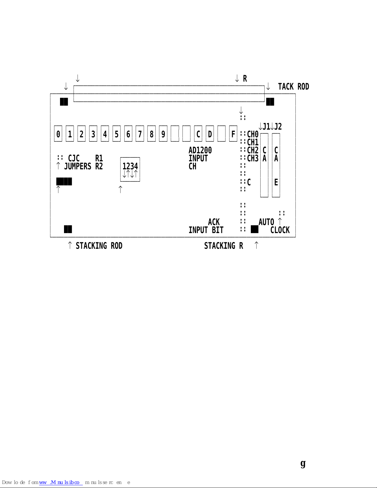
Analog Relay Mux Board Reference
Figure 1-1. AD1200 Card Layout._____________________________
Original Version Without ISO122 Amp.
STACK æ RELAY 0
æ
RELAY 15
ROD
æ ЪДДДДДДДДДДДДДДДДДДДДДДДДДДДДДДДДДДДДДДДДДДДДДДДД¿ж
STACK ROD
ЪДДДДДЕДДДДДДДДДДДДДДДДДДДДДДДДДДДДДДДДДДДДДДДДДДДДДДДДЕДДДДДДД¿
³
ÛÛ АДДДДДДДДДДДДДДДДДДДДДДДДДДДДДДДДДДДДДДДДДДДДДДДДЩЫЫ ³
³
æ
W34
³
³
þþ ³
³ÚÄ¿ÚÄ¿ÚÄ¿ÚÄ¿ÚÄ¿ÚÄ¿ÚÄ¿ÚÄ¿ÚÄ¿ÚÄ¿ÚÄ¿ÚÄ¿ÚÄ¿ÚÄ¿ÚÄ¿ÚÄ¿
æJ1æ
J2
³
³³
0
³³1³³2³³3³³4³³5³³6³³7³³8³³9³³A³³B³³C³³D³³E³³F³þþ
CH0
ÚÄ¿ÚÄ¿ ³
³АДЩАДЩАДЩАДЩАДЩАДЩАДЩАДЩАДЩАДЩАДЩАДЩАДЩАДЩАДЩАДЩюю
CH1³
³³ ³³
³
AD1200
þþ
CH2³C
³³C³³
³
þþ
CJC R1
ЪДДДД¿
INPUT
þþ
CH3³A
³³A³³
³
å JUMPERS R2
³
1234
³
CHANNEL
þþ
CH4³B
³³B³³
³
R3
³æåæå³
SELECT
þþ
CH5³L
³³L³³
³
ÛÛÛÛ
R4
АДДДДЩ
þþ
CH6³E
³³E³³
³
å POT R23
å
CARD
þþ
CH7³
³³ ³³
³
ADDRESS
АДЩАДЩ ³
³
RELAY
þþ ³
³
MADE
þþ
ADC
þþ ³
³
FEEDBACK
þþ
AUTO
å³
³
ÛÛ
INPUT BIT
þþ ÛÛ
CLOCK
³
АДДДДДДДДДДДДДДДДДДДДДДДДДДДДДДДДДДДДДДДДДДДДДДДДДДДДДДДДДДДДДДЩ
å
STACKING ROD STACKING ROD
å
Page 3
Page 7
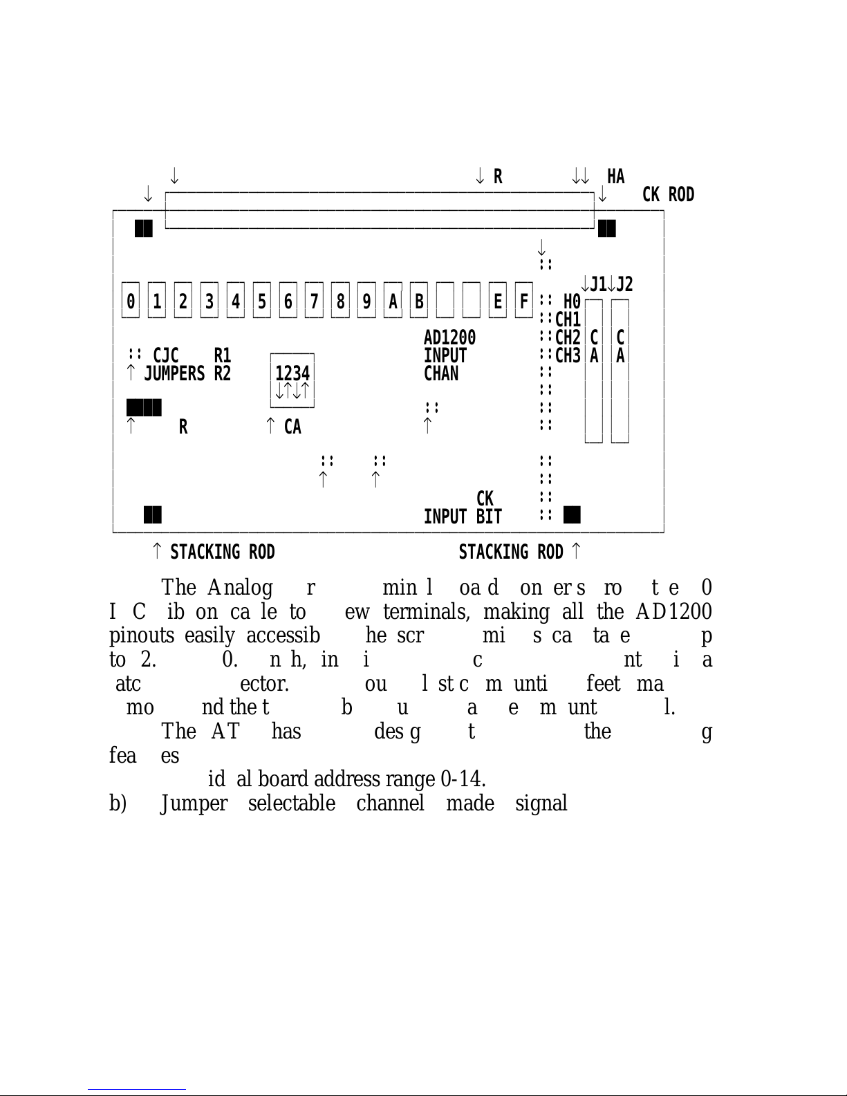
Reference Analog Relay Mux Board
Figure 1-2. AD1200 Card Layout._____________________________
Updated Version With ISO122 Amp.
STACK æ RELAY 0
æ
RELAY 15
ææ
CHAIN OUT
ROD
æ ЪДДДДДДДДДДДДДДДДДДДДДДДДДДДДДДДДДДДДДДДДДДДДДДДД¿ж
STACK ROD
ЪДДДДДЕДДДДДДДДДДДДДДДДДДДДДДДДДДДДДДДДДДДДДДДДДДДДДДДДЕДДДДДДД¿
³
ÛÛ АДДДДДДДДДДДДДДДДДДДДДДДДДДДДДДДДДДДДДДДДДДДДДДДДЩЫЫ ³
³
æ
W34
³
³
þþ ³
³ÚÄ¿ÚÄ¿ÚÄ¿ÚÄ¿ÚÄ¿ÚÄ¿ÚÄ¿ÚÄ¿ÚÄ¿ÚÄ¿ÚÄ¿ÚÄ¿ÚÄ¿ÚÄ¿ÚÄ¿ÚÄ¿
æJ1æ
J2
³
³³
0
³³1³³2³³3³³4³³5³³6³³7³³8³³9³³A³³B³³C³³D³³E³³F³þþ
CH0
ÚÄ¿ÚÄ¿ ³
³АДЩАДЩАДЩАДЩАДЩАДЩАДЩАДЩАДЩАДЩАДЩАДЩАДЩАДЩАДЩАДЩюю
CH1³
³³ ³³
³
AD1200
þþ
CH2³C
³³C³³
³
þþ
CJC R1
ЪДДДД¿
INPUT
þþ
CH3³A
³³A³³
³
å JUMPERS R2
³
1234
³
CHANNEL
þþ
CH4³B
³³B³³
³
R3
³æåæå³
SELECT
þþ
CH5³L
³³L³³
³
ÛÛÛÛ
R4
АДДДДЩ þþ
þþ
CH6³E
³³E³³
³
å POT R23
å
CARD
å
ADCLOCK
þþ
CH7³
³³ ³³
³
ADDRESS
АДЩАДЩ ³
³
þþ þþ
RELAY
þþ ³
³
å
GAINåVOPT MADE
þþ ³
³
FEEDBACK
þþ ³
³
ÛÛ
INPUT BIT
þþ ÛÛ ³
АДДДДДДДДДДДДДДДДДДДДДДДДДДДДДДДДДДДДДДДДДДДДДДДДДДДДДДДДДДДДДДЩ
å
STACKING ROD STACKING ROD
å
The Analog Screw Terminal Board converts from the 50
IDC ribbon cable to screw terminals, making all the AD1200
pinouts easily accessible. The screw terminals can take wire up
to 2.5mm, 0.1 inch, in diameter. Each of 50IDC entry is a
latching connector. The four plastic mounting feet may be
removed and the terminal board used as a screw mounted panel.
The ATB has been designed to provide the following
features:a) Individual board address range 0-14.
b) Jumper selectable channel made signal Feedback to
AD1200 card via digital input port.
c) Jumper enabled channel made signal Feedback to AD1200
card via A/D clock input allowing next A/D conversion to
be automatically triggered.
d) Provision for cold junction compensation circuitry, CJC, for
thermocouple inputs, jumper switched via relay 0.
e) Twin 50 way D connector ribbon cables allows for easy
daisy chaining of multiple boards.
Page 4
Page 8
Analog Relay Mux Board Reference
f) Twin 50 way D connector ribbon cables allows for easy
daisy chaining of multiple boards.
Card Address DIP Switches._________________________
The Card Address DIP switches t jumpers determine to
which channel on the PC A/D card the output of the relays is
routed.
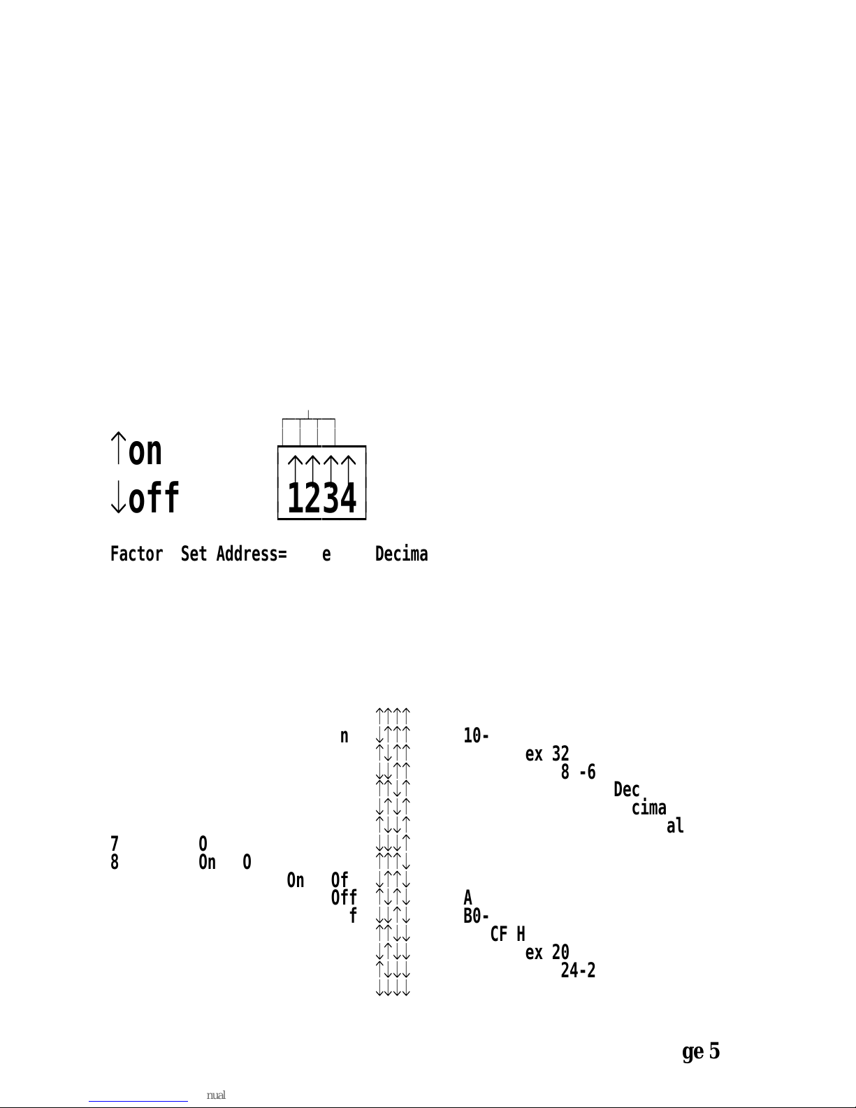
Figure 1-3. ADMUX Factory Set Address DIPs._________________________________________
DIP 1-4 Mux Board Address select
ЪДВБВД¿
³ý³ý³ý³
å
on
ЪДДДД¿
³åååå³
æ
off
³
1234
³
АДДДДЩ
Factory Set Address= 0 Hex, 0 Decimal
Relays chosen by putting 00-0F Hex, 0-15 decimal on Digital out port.
Figure 1-4. ADMUX Board Addresses._________________________________
BOARD DIP DIP DIP DIP SWITCH Relays Addressed By_____ ___ ___ ___ ___ ______ ___________________
ADDRESS 1234
DO7 DO6 DO5 DO4
0 OnOnOnOn
åååå
00-0F Hex 0 -15 Dec Default
1 Off On On On
æååå
10-1F Hex 16 -31 Decimal
2 On Off On On
åæåå
20-2F Hex 32 -47 Decimal
3 Off Off On On
ææåå
30-3F Hex 48 -63 Decimal
4 On On Off On
ååæå
40-4F Hex 64 -79 Decimal
5 Off On Off On
æåæå
50-5F Hex 80 -95 Decimal
6 On Off Off On
åææå
60-6F Hex 96 -111 Decimal
7 Off Off Off On
æææå
70-7F Hex 112-127 Decimal
8 OnOnOnOff
åååæ
80-8F Hex 128-143 Decimal
9 Off On On Off
æååæ
90-9F Hex 144-159 Decimal
10 On Off On Off
åæåæ
A0-AF Hex 160-175 Decimal
11 Off Off On Off
ææåæ
B0-BF Hex 176-191 Decimal
12 On On Off Off
ååææ
C0-CF Hex 192-207 Decimal
13 Off On Off Off
æåææ
D0-DF Hex 208-223 Decimal
14 On Off Off Off
åæææ
E0-EF Hex 224-239 Decimal
15 Off Off Off Off
ææææ
Do Not Use!
Page 5
Page 9
Reference Analog Relay Mux Board
AD1200 Input Channel Select Jumpers.__________________________________
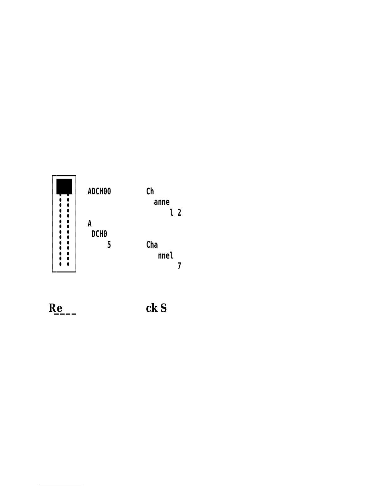
The AD1200 input channel select jumpers determine to
which channel on the PC A/D card the output of the relays is
routed. The A/D conversion are then performed with this channel
selected on the PC AD1200 card. Since the relays are switching
differential signals two jumpers are used to select A/D input
channel, the Channel and its return line. In differential mode
there are 8 possible input channels for the A/D converter.
Figure 1-5. AD1200 Input Channel Select.____________________________________
JUMPER LABEL ADC Channel Selected______ _____ ____________________
ÚÄÄ¿
³ÛÛ³
ADCH00 Channel 0 DEFAULT
³þþ³
ADCH01 Channel 1
³þþ³
ADCH02 Channel 2
³þþ³
ADCH03 Channel 3
³þþ³
ADCH04 Channel 4
³þþ³
ADCH05 Channel 5
³þþ³
ADCH06 Channel 6
³þþ³
ADCH07 Channel 7
ÀÄÄÙ
Relay Made Feedback Select Jumpers._________________________________
The ADMUX board has break before make circuitry. There
is a time delay after outputting the address on the digital output
port before the previously made relay breaks and the newly the
selected relay makes and the analog input is switched through to
the AD1200 channel. To ensure that sufficient time elapses
before the A/D conversion is taken a relay made signal can be
fed back from the ADMUX board on to one of the bits of the
AD1200 digital input port. Software should poll this port waiting
for the correct bit to go LOW before the A/D conversion is
triggered. Only place one jumper on these pins.
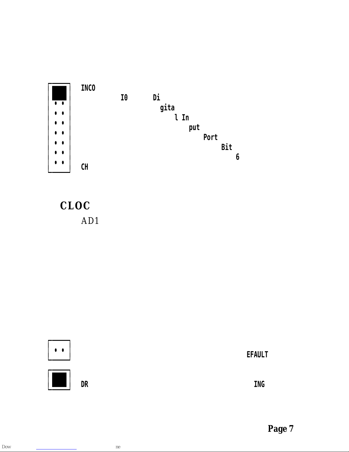
The legend on the ADMUX board is incorrect in labelling the
line CH0, CH1 etc. They should be labelled DI0, DI1 for Digital
Page 6
Page 10
Analog Relay Mux Board Reference
Input Bit 0 etc.
Figure 1-6. Relay Made Feedback Jumper._____________________________________
JUMPER LABEL LABEL FEEDBACK BIT______ _____ _____ ____________
ÚÄÄ¿
INCORRECT RIGHT
³ÛÛ³
CH0 DI0 Digital Input Port Bit 0 DEFAULT
³ùù³
CH1 DI1 Digital Input Port Bit 1
³ùù³
CH2 DI2 Digital Input Port Bit 2
³ùù³
CH3 DI3 Digital Input Port Bit 3
³ùù³
CH4 DI4 Digital Input Port Bit 4
³ùù³
CH5 DI5 Digital Input Port Bit 5
³ùù³
CH6 DI6 Digital Input Port Bit 6
³ùù³
CH7 DI7 Digital Input Port Bit 7
ÀÄÄÙ
ADCLOCK Jumper.__________________
The AD1200 series cards have an external clock input line
EXT CLOCK, that can be used to strobe A/D conversions when
the card is in mode 3. The EXT CLOCK line must be driven by
a high to low going edge. The ADMUX card’s relay made feed
back signal can be used to drive this input so allowing the A/D
converter to automatically start an A/D conversion as soon as the
relays have switched through the input signal. The ADMUX
card’s line is tristated and so several boards can all be jumpered
onto the AD1200 input, each board driving it as it is selected.
Figure 1-7. ADCLOCK Jumper.____________________________
JUMPER FUNCTION______ ________
ÚÄÄ¿
³ùù³
NOT DRIVING AD1200 EXTERNAL CLOCK INPUT DEFAULT
ÀÄÄÙ
ÚÄÄ¿
³ÛÛ³
DRIVING AD1200 EXTERNAL CLOCK INPUT - AUTO CLOCKING
ÀÄÄÙ
Page 7
Page 11
Reference Analog Relay Mux Board
Cold Junction Compensation.__________________________
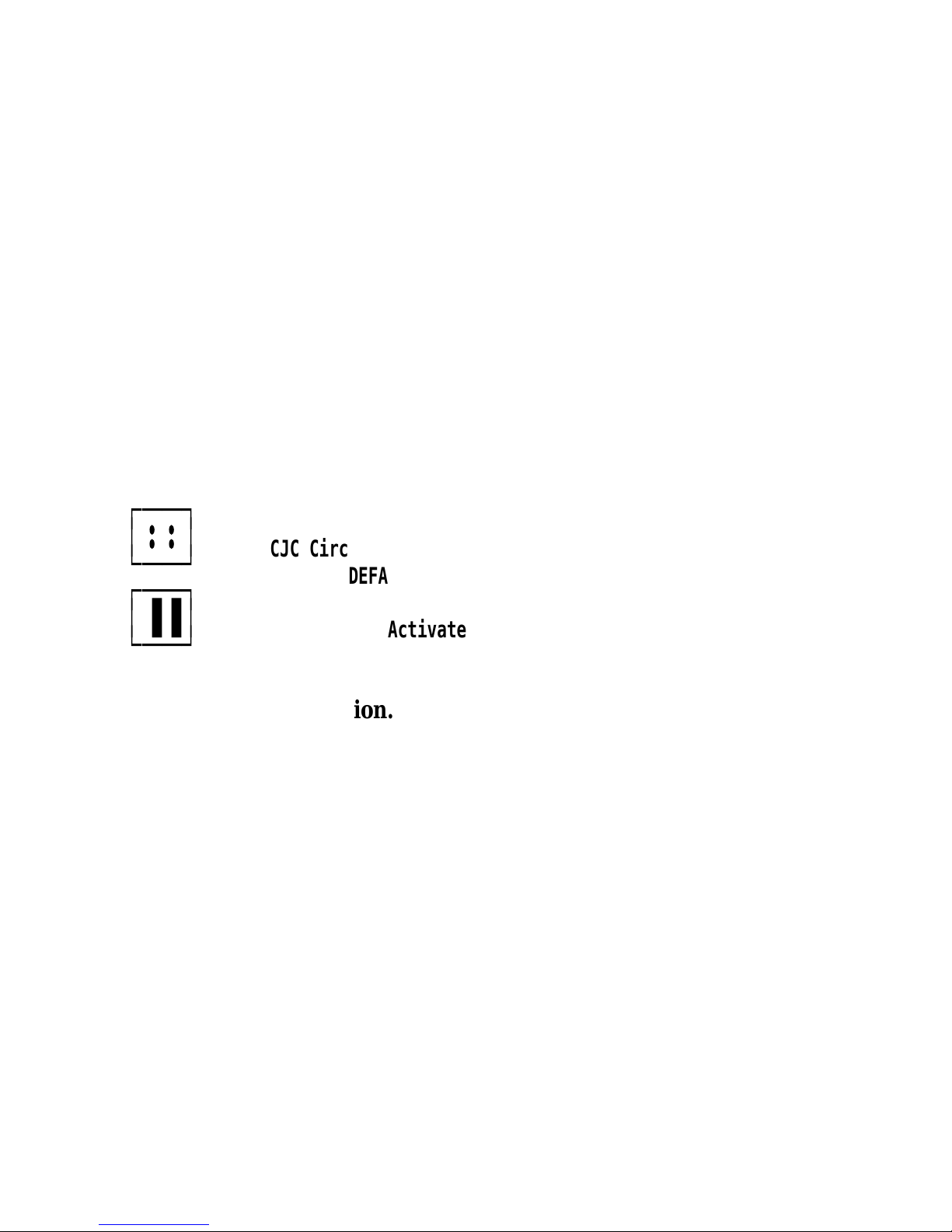
The ADMUX card has on board cold junction compensation
circuitry. When the two jumper links are connected the Cold
Junction Circuit is connected to Relay 0 on the ADMUX board.
When the two jumper links are removed then Relay 0 is free for
use as a normal input. Do not wire any other inputs to Relay 0
on those boards where the CJC circuitry has been activated. The
jumpers connect Relay 0 input to the cold junction circuit and
Relay 0 return line to ANALOG ground.
The Cold Junction Compensation jumpers are located on the
middle left hand side of the ADMUX board and are labelled
CJC TO REL00 ENABLE.
Figure 1-8. Activating Cold Junction Compensation._____________________________________________
ÚÄÄ¿
³þþ³
CJC Circuit Unused. Relay 0 free for normal use.
ÀÄÄÙ
FACTORY DEFAULT.
ÚÄÄ¿
³ÞÞ³
CJC Circuit Activated On Relay 0.
ÀÄÄÙ
Using The Cold Junction.
The cold junction, like thermocouples, is usually used in
Differential Input mode. The cold junction circuitry is connected
by jumpers W1 and W2 to the Analog Input Channel 0 and
Channel 0 Return lines. R26, need not be inserted when the CJC
circuitry is in use. When jumpers are not placed across the W1
and W2 shorting headers the cold junction compensation
circuitry does not effect the analog terminal board or the
AD1200 card at all.
The CJC circuitry produces 0.5mVolts per degree Centigrade,
thus by performing an A/D conversion on channel 0 the
temperature of the thermocouples cold junction is known and the
apparent temperature measured by the thermocouple can be
adjusted so that the true temperature of the thermocouple is
known.
Page 8
Page 12

Analog Relay Mux Board Reference
Example:
AD1200 card jumper set range of 0-10 Volts unipolar.
Gain of 1000 is selected for Channel 0
Ambient temperature of 18 degrees Centigrade
Thus CJC circuit gives a voltage of 18 x 0.5 mV = 9mV.
9mV input Channel 0 at gain of 1000 equivalent to 9 Volts
9 Volts on 0-10V i/p range is 9*4096/10= 3686= E66hex
To convert a reading into a temperature in degrees Centigrade
use the following formula:Temp in C = (ADC Reading * Input Span In Volts)_______________________________
(4096 * Gain * 0.5mV per C)
where the 0.5mV per degree C is 0.5/1000 Volts per degree C.
Thus for the above ADC reading of 3686 decimal, with a 10Volt
span in the input range and a Gain of 1000.
Temp in C= ( 3686 * 10)__________
(4096 * 1000 * 0.5/1000 )
Temp in C= ( 36860) = 18 degrees] Centigrade._______
(2048 )
Calibrating The Cold Junction.
The cold junction compensation circuit can be calibrated simply
in the following manner. Place a precision voltmeter across the
CJC TO REL0 ENABLE jumper pins. Adjust potentiometer R23
with a screw driver so that the voltmeter reads 0.5mV times the
ambient temperature. Thus if the room temperature is 20 degree
C, R23 should be adjusted till the voltmeter reads exactly
10mVolts.
Page 9
Page 13

Reference Analog Relay Mux Board
Resistors R1, R2, R3 and R4._________________________
There is provision for adding four optional resistors to the
ADMUX card.
R1 Precision 250 Ohms resistor. Diff Current Input Only!
Fit this when using the ADMUX card with 4-20m Amp
differential current inputs. Omit for thermocouple use.
R2 Nominally 10k Ohms
Fit with 10k nominal resistor to provide differential return
path to analog ground. This reference the Differential Input
signal to the ground on the AD1200 card. Omit when using
with the ISO122 isolation amplifier.
R2 Precision 250 Ohms Single Ended Current Inputs only!
When using the relays for switching single ended current
input signals fit 250 Ohm precision resistor for 4-20m Amp
current to voltage conversion.
R3 Nominally 100M Ohms
This is for thermocouple break detection. When this resistor
is fitted, if the thermocouple breaks or if an open circuit
input is switched in the input line is pulled up to +2Volts.
See also VOPT jumpers and R14 below.
R4 Precision 250 Ohms Single Ended Current Inputs only!
Fit this when using the ADMUX card with 4-20m Amp
differential current inputs. is the current to voltage shunt
Omit for thermocouple use.
Jumpers W3 and W4.___________________
Jumpers W3 and W4 should be left in place when using the
relays to switch differential inputs through to the AD1200 card.
Jumper W3 connects the system ground, SYS GND, to the
ANALOG ground. Single Ended inputs normally have a return
path via analog ground and this jumper connects the analog
ground to SYS GND.
Page 10
Page 14

Analog Relay Mux Board Reference
Jumper W4 connects the AMPLOW to the ANALOG ground.
Pseudo differential inputs are referenced to AMPLOW. This
jumper can be used in conjunction to W3 to connect AMP LOW
to the system ground SYS GND.
Low Pass Filter, R15 and C28.__________________________
The input to the programmable gain amp passes through a
low pass filter formed by R15 and C28. The nominal value of
these is R15 1k2 = 1200 Ohms, and C28 = 1.0uF. This produces
a time constant of approx 1/1000 second, cutting off signal
above 1kHz. To disable this remove C28 and short out R15.
R15 and C28 are located between the NMH1215 DC/DC
converter and the PGA202 amplifier. Just to the right of the
VOPT jumpers.
Gain Setting of Signal Amplifier._____________________________
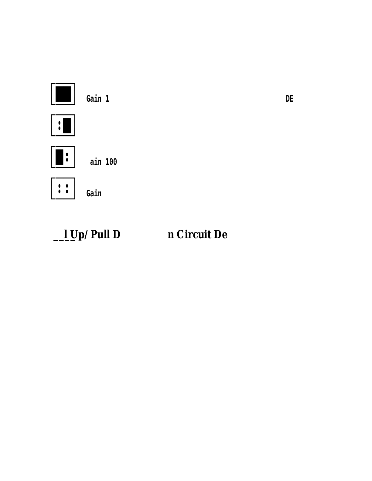
The PGA202 provides 4 jumper selected amplifications for
the signal before passing to the isolation amplifier.
The two GAIN jumpers are located in the centre of the
ADMUX card. The gain is the factor by which the input signal
from the on board relays or the CHAIN IN connection is
amplified by before isolation. The on board CJC compensation
produces a voltage of approx 10mV at room temperature, with a
gain of 100 jumper selected a 1 Volt signal is will be passed on
to the isolation amp and thence to the AD1200 card.
Page 11
Page 15
Reference Analog Relay Mux Board
Figure 1-9. Gain Selection._______________________
GAIN Gain Selected______ ____________
ÚÄÄ¿
³ÛÛ³
Gain 1 DEFAULT
ÀÄÄÙ
ÚÄÄ¿
³þÛ³
Gain 10
ÀÄÄÙ
ÚÄÄ¿
³Ûþ³
Gain 100
ÀÄÄÙ
ÚÄÄ¿
³þþ³
Gain 1000
ÀÄÄÙ
Pull Up/ Pull Down- Open Circuit Detection._______________________________________
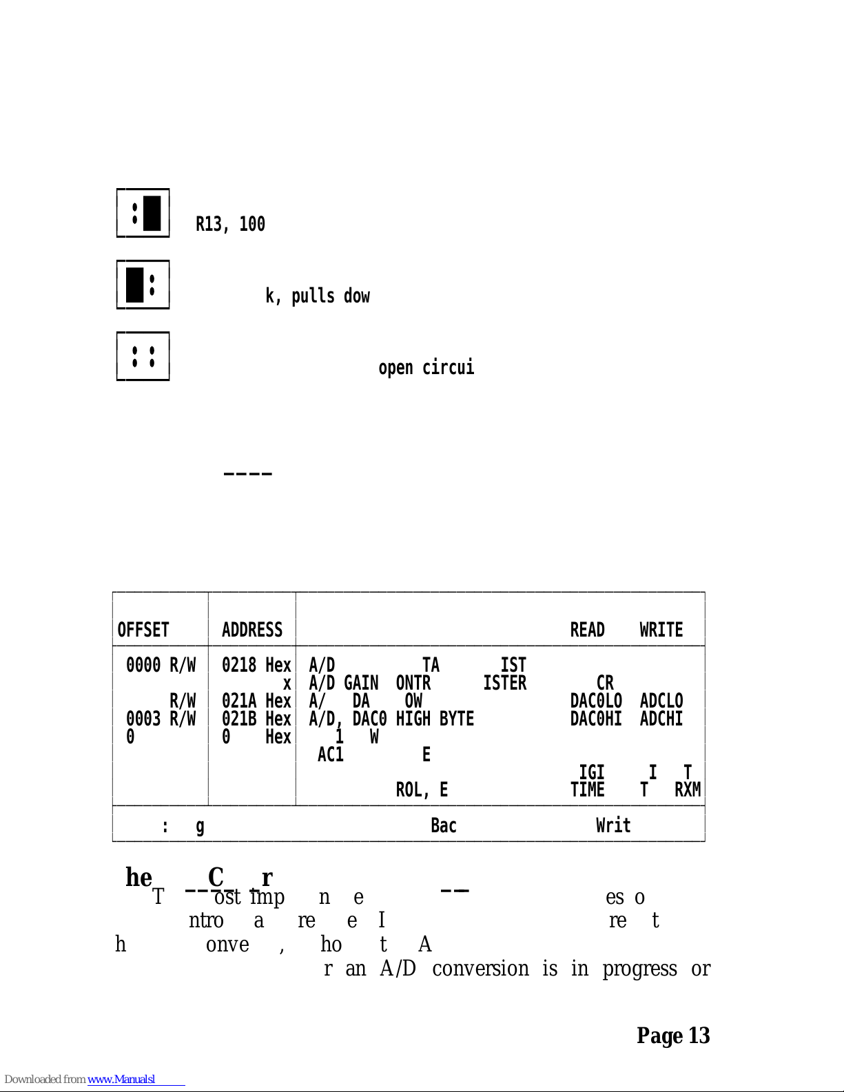
Open circuit inputs can be detected by the installation of
resistors to pull the differential input lines to a known state
The two VOPT jumpers can pull the INPUT+ line, via a 100k
resistor R13, to isolated grounds or to the isolated +15volt
supply. To disconnect this pull up/down remove both jumpers.
Resistor R14 pull the INPUT- line to the isolated ground level in
the event of floating inputs. To disconnect this pull down
remove R14.
Page 12
Page 16
Analog Relay Mux Board Reference
Figure 1-10. VOPT Selection.__________________________
VOPT Connection Of INPUT+ line.______ _________________________
ÚÄÄ¿
³þÛ³
R13, 100k, pulls up to isolated +15volts.
ÀÄÄÙ
ÚÄÄ¿
³Ûþ³
R13, 100k, pulls down to isolated Ground.
ÀÄÄÙ
ÚÄÄ¿
³þþ³
R13 Disconnected, No open circuit detect on INPUT+.
ÀÄÄÙ
AD1200 Register Resume._______________________
The register of the AD1200 card are now quickly listed as
an aide to explaining the sample program.
Figure 1-11. AD1200 Register Map._______________________________
ЪДДДДДДДДДДВДДДДДДДДДВДДДДДДДДДДДДДДДДДДДДДДДДДДДДДДДДДДДДДДДДДДДДДД¿
³
ADDRESS
³ý
DEFAULT
ý³ý
REGISTER
ээээээээээ
ýý³
³
OFFSET
ýýýý³ý
ADDRESS
ý³
эээээээээээээ
ýýý
READ
ýýý
WRITE
ýý³
ГДДДДДДДДДДЕДДДДДДДДДЕДДДДДДДДДДДДДДДДДДДДДДДДДДДДДДДДДДДДДДДДДДДДДД´
³ý
0000ýR/W
ý³ý
0218ýHex³ A/D CONTROL STATUS REGISTER
ý
ADCSR ADCSR
ý³
³ý
0001ýR/W
ý³ý
0219ýHex³ A/D GAIN CONTROL REGISTER ADGCR
ý
ADGCR
³
³ý
0002ýR/W
ý³ý
021AýHex³ A/D, DAC0 LOW BYTE
ýýýý ý
DAC0LO ADCLO
ý³
³ý
0003ýR/W
ý³ý
021BýHex³ A/D, DAC0 HIGH BYTE
ýýýý ý
DAC0HI ADCHI
ý³
³ý
0004
ýýýWý³ý
021CýHex³ DAC1 LOW BYTE
ýýýý ý
DAC1LO
ý³
³ý
0005
ýýýWý³ý
021DýHex³ DAC1 HIGH BYTE
ýýýý ý
DAC1HI
ý³
³ý
0006ýR/W
ý³ý
021EýHex³ DIGITAL I/O PORT
ýý
ýDIGIN ýDIGOUT
ý³
³ý
0007ýR/W
ý³ý
021FýHex³ TIMER CONTROL, EXTENDED MODE TIMERXM TIMERXM
³
ГДДДДДДДДДДБДДДДДДДДДБДДДДДДДДДДДДДДДДДДДДДДДДДДДДДДДДДДДДДДДДДДДДДД´
³ý
Note: Registers Do Not Always Read Back What Has Been Written
ý³
АДДДДДДДДДДДДДДДДДДДДДДДДДДДДДДДДДДДДДДДДДДДДДДДДДДДДДДДДДДДДДДДДДДДЩ
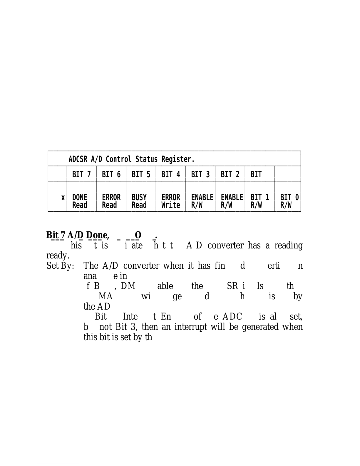
The A/D Control Status Register._____________________________
The most important register in the AD1200 series of cards
is the control status register. It is the primary control register for
the AD Converter, it holds the A/D Busy and A/D Done bits
which indicate whether an A/D conversion is in progress or
Page 13
Page 17
Reference Analog Relay Mux Board
finished, its A/D Error and Clear Error bits are used to detect
and service A/D overrun or triggering mistakes. The DMA and
Interrupt enable bits are used to decide whether the A/D Done
bit causes a DMA read or system interrupt. Finally its Mode bits
determine whether single shot or continuous A/D conversions are
performed and what initiates the repetitive conversions and at
what rate they occur.
Figure 1-12. A/D Control Status Register.____________________________________
ЪДДДДДДДДДДДДДДДДДДДДДДДДДДДДДДДДДДДДДДДДДДДДДДДДДДДДДДДДДДДДДДДДДДД¿
³эээээ
ADCSR A/D Control Status Register.
ээээээээээээээээээ³
ГДДДДВДДДДДДДВДДДДДДДВДДДДДДДВДДДДДДДВДДДДДДДВДДДДДДДВДДДДДДДВДДДДДД´
³
³ý
BITý7
ý³ý
BITý6
ý³ý
BITý5
ý³ý
BITý4
ý³ý
BITý3
ý³ý
BITý2
ý³ý
BITý1
ý³ý
BITý0
³
ГДДДДЕДДДДДДДЕДДДДДДДЕДДДДДДДЕДДДДДДДЕДДДДДДДЕДДДДДДДЕДДДДДДДЕДДДДДД´
³
0218
³ý
A/D
ýý³ý
A/D
ýý³ý
A/D
ýý³ý
CLEAR
ý³ý
DMA
ýý³ý
INT
ýý³ý
MODE
ýý³ý
MODE
ý³
³ý
Hex
³ý
DONE
ý³ý
ERROR
ý³ý
BUSY
ý³ý
ERROR
ý³ý
ENABLE
³ý
ENABLE³ BIT 1
ý³ý
BIT 0
³
³ýýýý³ý
Read
ýý³ý
Read
ýý³ý
Read
ýý³ý
Write
ý³ý
R/W
ýýý³ý
R/W
ýýý³ý
R/W
ýýý³ý
R/W
ýý³
АДДДДБДДДДДДДБДДДДДДДБДДДДДДДБДДДДДДДБДДДДДДДБДДДДДДДБДДДДДДДБДДДДДДЩ
Bit 7 A/D Done, Read Only.________________________
This bit is indicates that the A/D converter has a reading
ready.
Set By: The A/D converter when it has finished converting an
analogue input.
If Bit 3, DMA Enable, of the ADCSR is also set then
a DMA cycle will be generated when this bit is set by
the ADC.
If Bit 2, Interrupt Enable, of the ADCSR is also set,
but not Bit 3, then an interrupt will be generated when
this bit is set by the ADC.
Reset By:
Reading the ADC data high byte at Register 3.
This bit is automatically cleared at power up.
Page 14
Page 18
Analog Relay Mux Board Reference
The A/D Gain Channel Register.____________________________
The A/D Gain Channel Register, ADGCR, is used to select
the input channel to the A/D converter and the gain applied to
the input signal by the programmable gain amplifier.
When in Mode 0, single conversion mode, then writing to the
A/D Gain Channel Register forces the A/D Converter to start its
next conversion.
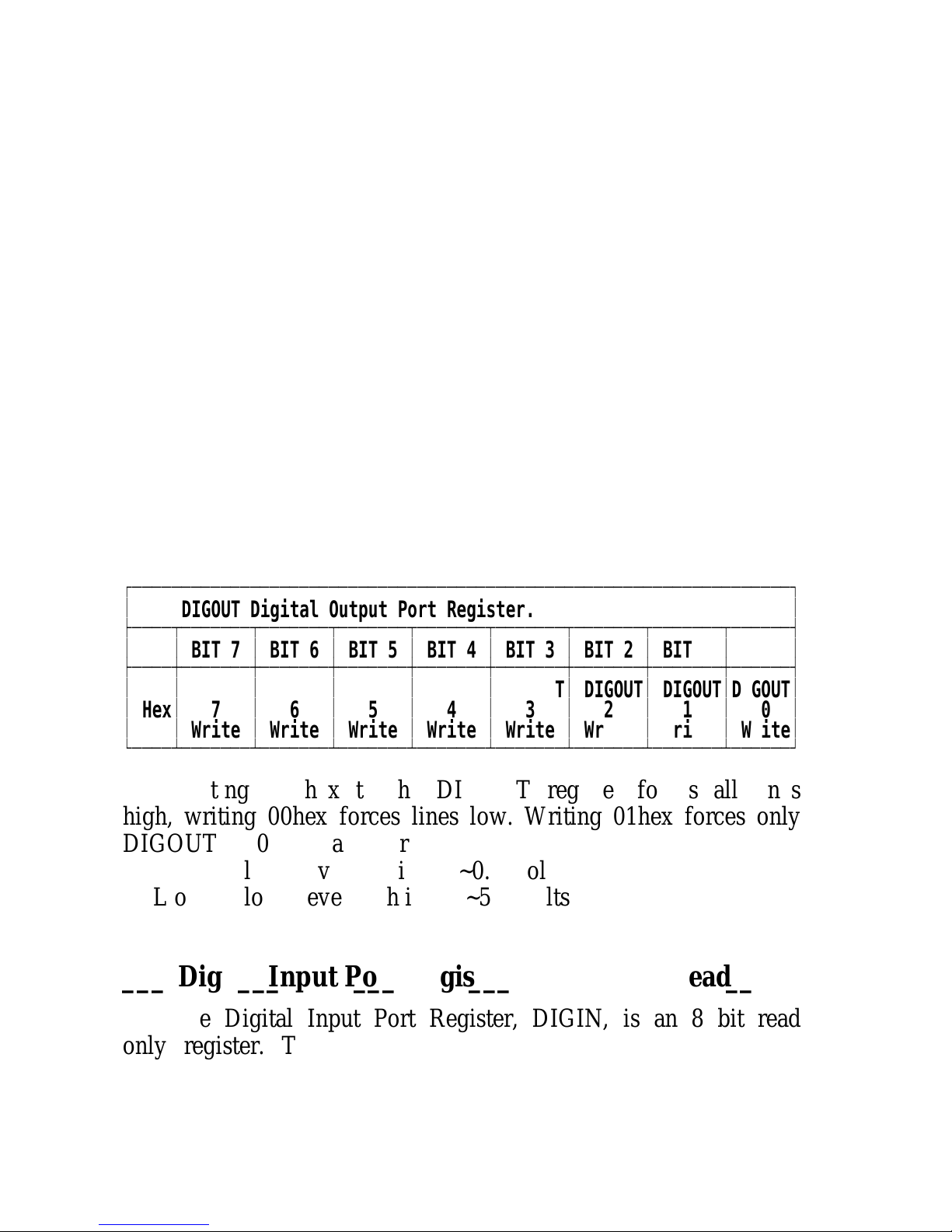
The Digital Output Port Register. Write Only_____________________________ __________
The Digital Output Port Register, DIGOUT, is an 8 bit
write only register. The bit values written correspond exactly
with the on/off logic state of the 8 TTL output lines. Thus bits
set true force the corresponding DIGOUT line high, those bits
set false force the DIGOUT line low.
Figure 1-13. DIGOUT Output Register.__________________________________
ЪДДДДДДДДДДДДДДДДДДДДДДДДДДДДДДДДДДДДДДДДДДДДДДДДДДДДДДДДДДДДДДДДДДД¿
³эээээ
DIGOUT Digital Output Port Register.
ээээээээээээээээ
ýý³
ГДДДДВДДДДДДДВДДДДДДДВДДДДДДДВДДДДДДДВДДДДДДДВДДДДДДДВДДДДДДДВДДДДДД´
³
³ý
BITý7
ý³ý
BITý6
ý³ý
BITý5
ý³ý
BITý4
ý³ý
BITý3
ý³ý
BITý2
ý³ý
BITý1
ý³ý
BITý0
³
ГДДДДЕДДДДДДДЕДДДДДДДЕДДДДДДДЕДДДДДДДЕДДДДДДДЕДДДДДДДЕДДДДДДДЕДДДДДД´
³
021E³ DIGOUT³ DIGOUT³ DIGOUT³ DIGOUT³ DIGOUT³ DIGOUT³ DIGOUT³DIGOUT
³
³ý
Hex
³ý
7
ý³ý
6
ý³ý
5
ý³ý
4
ý³ý
3
ý³ý
2
ý³ý
1
ý³ý
0
ý³
³ýýýý³ý
Write
ý³ý
Write
ý³ý
Write
ý³ý
Write
ý³ý
Write
ý³ý
Write
ý³ý
Write
ý³
Write
³
АДДДДБДДДДДДДБДДДДДДДБДДДДДДДБДДДДДДДБДДДДДДДБДДДДДДДБДДДДДДДБДДДДДДЩ
Writing 0FFhex to the DIGOUT register forces all lines
high, writing 00hex forces lines low. Writing 01hex forces only
DIGOUT bit 0 high, all the rest are low.
TTL output logic level low is 0.0 ~0.8 Volts.
TTL output logic level high is 2.4 ~5.0 Volts.
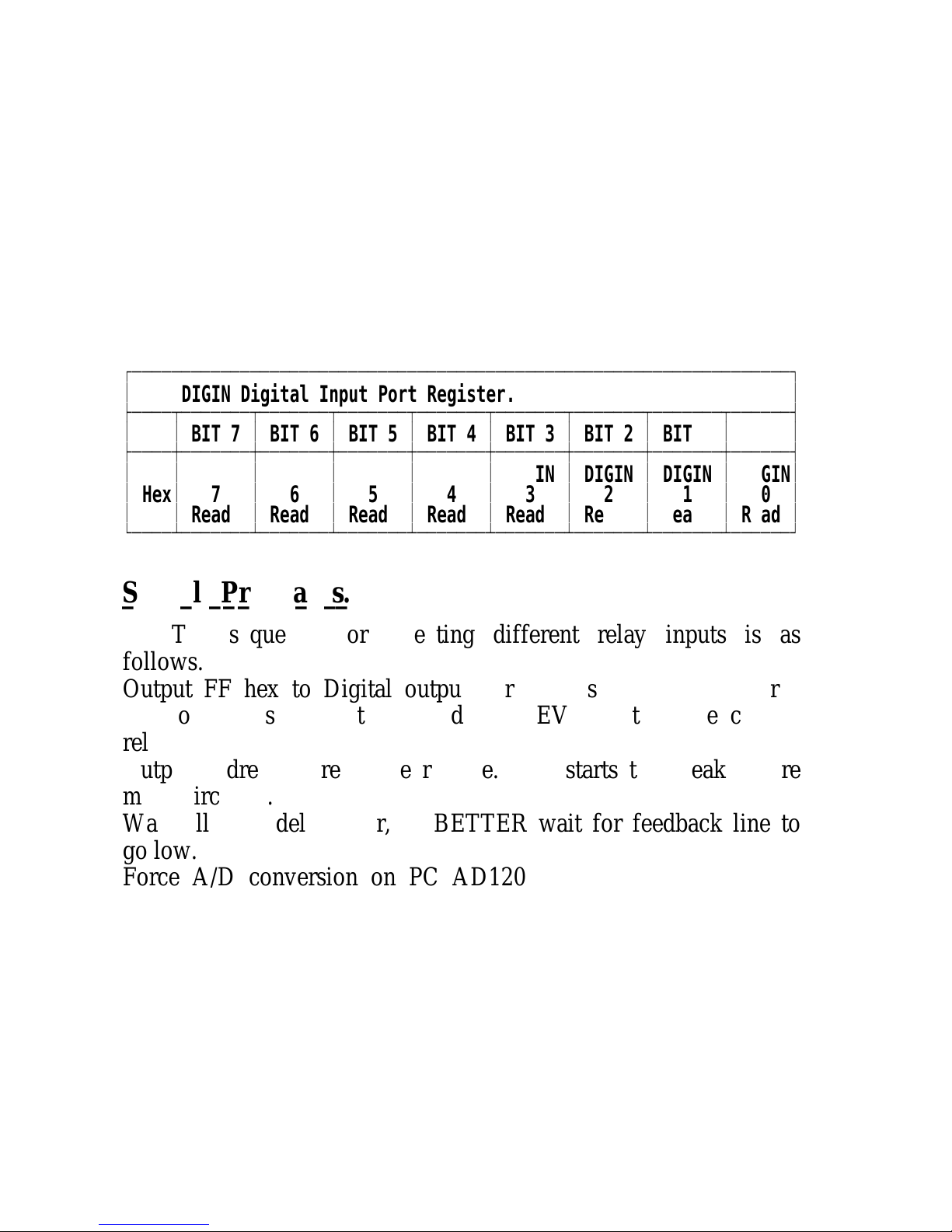
The Digital Input Port Register. Read Only____________________________ __________
The Digital Input Port Register, DIGIN, is an 8 bit read
only register. The bit values read represent the logic levels
present on the 8 TTL input lines. Thus lines that are high cause
the corresponding DIGIN bit to read high, those lines that are
Page 15
Page 19
Reference Analog Relay Mux Board
low cause the corresponding DIGIN bit to read low. If on
reading the DIGIN register a value of 0FFhex is obtained then
all the TTL input lines where true. A reading of 00hex means
that all lines were low. A reading of 01hex means that only
DIGIN line 0 was high, all the rest are low.
TTL output logic level low is 0.0 ~0.8 Volts.
TTL output logic level high is 2.4 ~5.0 Volts.
Figure 1-14. DIGIN Output Register.________________________________
ЪДДДДДДДДДДДДДДДДДДДДДДДДДДДДДДДДДДДДДДДДДДДДДДДДДДДДДДДДДДДДДДДДДДД¿
³эээээ
DIGIN Digital Input Port Register.
ээээээээээээээээ
ý
ý³
ГДДДДВДДДДДДДВДДДДДДДВДДДДДДДВДДДДДДДВДДДДДДДВДДДДДДДВДДДДДДДВДДДДДД´
³
³ý
BITý7
ý³ý
BITý6
ý³ý
BITý5
ý³ý
BITý4
ý³ý
BITý3
ý³ý
BITý2
ý³ý
BITý1
ý³ý
BITý0
³
ГДДДДЕДДДДДДДЕДДДДДДДЕДДДДДДДЕДДДДДДДЕДДДДДДДЕДДДДДДДЕДДДДДДДЕДДДДДД´
³
021E³ DIGIN ³ DIGIN ³ DIGIN ³ DIGIN ³ DIGIN ³ DIGIN ³ DIGIN ³ DIGIN
³
³ý
Hex
³ý
7
ý³ý
6
ý³ý
5
ý³ý
4
ý³ý
3
ý³ý
2
ý³ý
1
ý³ý
0
ý³
³ýýýý³ý
Read
ý³ý
Read
ý³ý
Read
ý³ý
Read
ý³ý
Read
ý³ý
Read
ý³ý
Read
³ý
Read
ý³
АДДДДБДДДДДДДБДДДДДДДБДДДДДДДБДДДДДДДБДДДДДДДБДДДДДДДБДДДДДДДБДДДДДДЩ
Sample Programs.________________
The sequence for selecting different relay inputs is as
follows.
Output FF hex to Digital output port to ensure all mux boards
are not addressed. Note Must do this EVERY time we change
relays.
Output address of relay we require. This starts the break before
make circuitry.
Wait till time delay over, or BETTER wait for feedback line to
go low.
Force A/D conversion on PC AD1200 by writing to ADGCR,
the channel that the mux board is driving. When ADDONE bit
set in ADGSR read ADCLO register first, then ADCHI register
next to retrieve the data.
Page 16
Page 20

Analog Relay Mux Board Reference
Figure 1-15. Sample Basic Program._______________________________
10 BASE=&H218: REM AD1200 BASE ADDRESS
11 W=2500: REM DELAY Time
12 ADCSR=BASE :ADGCR=BASE+1 :ADCLO=BASE+2 :ADCHI=BASE+3
13 DIGIN=BASE+6 :DIGOUT=BASE+6: REM Digital i/o ports at same address
14 FEED=&H1 :REM Relay Made Feedback Jumper Set To Bit 0 DEFAULT
15 :
16 :
20 FOR RELAY = 0 TO 15
25 OUT DIGOUT,&HFF: REM UNADDRESS ALL BOARDS
27:
30 OUT DIGOUT,RELAY: REM ADDRESS CHOSEN RELAY
35:
40 GOSUB 1000: REM Wait For FeedBack=Relay Closed
50:
60 FOR C=1 TO W :NEXT: REM Delay To Prevent Us Wasting RELAY’s Life
70 NEXT RELAY
80 :
90 END
99 :
100 REM FEEDBACK signal goes LOW when new relay made also on &H21E
1000 REM wait for feed back
1010 PRINT"Select Relay "RELAY " ";
1060 F=INP(DIGIN): REM Read Digital Input Port
1070 IF ( (F AND FEED)<>0) THEN GOTO 1060
1100 REM got feedback
1110 PRINT"Feedback Signal Received!";
1120:
1130:REM PERFORM A/D CONVERSION HERE
1140 OUT ADGCR,0: REM Select Channel Force Conversion
1150 IF ( (INP(ADCSR) AND 128)<>128) THEN GOTO 1150: REM Wait for AD
DONE
1160 LO=INP(ADCLO): REM Always Read Low Byte First
1170 HI=INP(ADCHI): REM And High Byte Last
1180 ADIN=HI*256 + LO: PRINT TAB(65)"A/D In="Hex$(ADIN)
1190:
1200 RETURN
5999 END
6000 SAVE "admux",A
Page 17
Page 21
Reference Analog Relay Mux Board
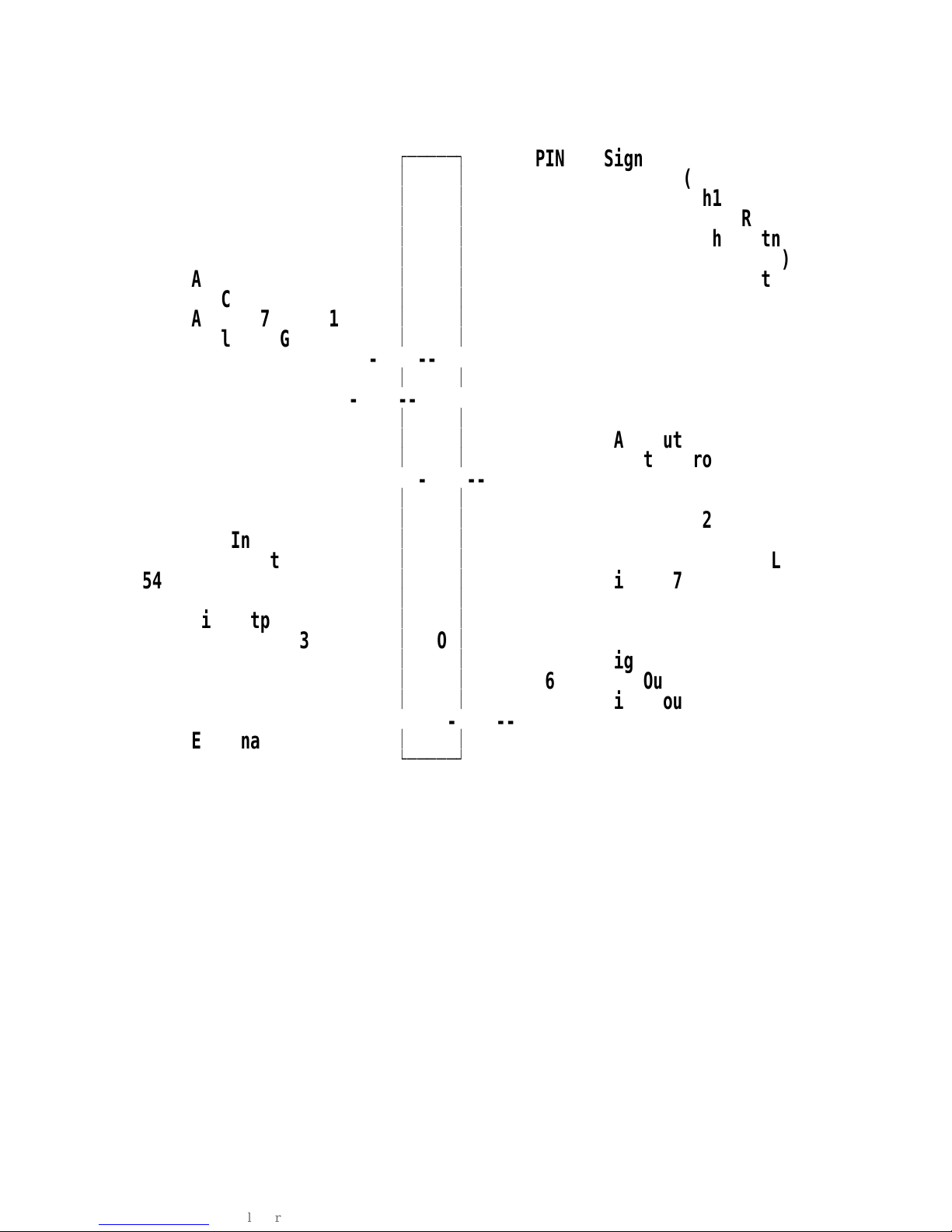
Figure 1-16. Relay Mux J1 & J2 Pin Outs.____________________________________
Signal PIN
ЪДДДДД¿
PIN Signal
AD Ch 0 1
³
1 2
ý³
2 AD Ch 8 (Ch0 Return)
AD Ch 1 3
³
3 4
ý³
4 AD Ch 9 (Ch1 Return)
AD Ch 2 5
³
5 6
ý³
6 AD Ch 10 (Ch2 Retn)
AD Ch 3 7
³
7 8
ý³
8 AD Ch 11 (Ch3 Retn)
AD Ch 4 9
³
O O
ý³
10 AD Ch 12 (Ch4 Retn)
AD Ch 5 11
³
O O
ý³
12 AD Ch 13 (Ch5 Retn)
AD Ch 6 13
³
O O
ý³
14 AD Ch 14 (Ch6 Retn)
AD Ch 7 15
³
O O
ý³
16 AD Ch 15 (Ch7 Retn)
Analogue Gnd 17
³
O O
ý³
18 Amp Low
------------------------------------------------------------+12Volts Out 19
³
O O
ý³
20 -12Volts Out
------------------------------------------------------------Power Ground 21
³
O O
ý³
22 DAC0 Output
DAC0 Ground 23
³
O O
ý³
24 DAC1 Output
DAC1 Ground 25
³
O O
ý³
26 Digital Ground
-----------------------------------------------------------Digital Gnd 27
³
O O
ý³
28 Dig Input 0
Dig Input 1 29
³
O O
ý³
30 Dig Input 2
Dig Input 3 31
³
O O
ý³
32 Dig Ground
Dig Input 4 33
³
O O
ý³
34 Dig In 5 / 8254 CLK0
8254 GATE0/ Dig In 6 35
³
O O
ý³
36 Dig In 7 / 8254 OUT0
Digital Gnd 37
³
O O
ý³
38 Dig Output 0
Dig Output 1 39
³
O O
ý³
40 Dig Output 2
Dig Output 3 41
³
O O
ý³
42 Dig Ground
Dig Output 4 43
³
O O
ý³
44 Dig Output 5
Dig Output 6 45
³
O O
ý³
46 Dig Output 7
Digital Gnd 47
³
O O
ý³
48 Dig Ground
-----------------------------------------------------------External Trigger
³
49 50
³
50 External Clock Input
Input
АДДДДДЩ
Page 18
Page 22

Index ADMUX Reference
Index.______
A/D control status reg.......13, 14
A/D Done.........................13, 14
A/D error..........................14
A/D gain channel reg........15
ADC..................................3, 6, 9, 14
ADCHI /LO......................13, 16
ADCSR.............................13, 14
ADGCR............................13, 15, 16
Base address.....................17
Cables...............................1, 4, 5
Channel select...................1, 2, 6
Clear error.........................14
Cold junction....................4, 8, 9
DAC0................................13, 18
DAC0 Ground..................18
DAC1................................13, 18
DAC1 Ground..................18
Differential.......................1, 2, 6, 8, 10, 11, 12
DIGIN...............................15, 16
Digital i/o..........................13, 17
Digital input......................4, 6, 7, 15, 16, 17
Digital output....................6, 15, 16
DIGOUT...........................15
DMA.................................14
Error..................................14
Extended mode.................13
External clock...................7, 18
External trigger.................18
Gain..................................1, 9, 11, 12, 13, 15
Isolation............................1, 2, 10, 11
Index Page 1
Page 23

ADMUX Reference Index
Make.................................6, 16
Mode 0..............................15
Mode 3..............................7
Multiplexer.......................1, 2
Multiplexing.....................1
Mux..................................5, 16, 18
Power................................14, 18
Programmable gain...........11, 15
Pseudo differential............11
Register map.....................13
Screw terminal board........4
Single conversion.............15
Single ended.....................10
Strobe................................7
Temperature......................8, 9, 11
Thermocouple...................4, 8, 10
TIMER..............................13
Trigger..............................18
Unipolar............................9
Version.............................3, 4
Voltmeter..........................9
Page 2 Index
 Loading...