BOURNS TISP7015 Service Manual

TISP7015
VERSIONS
*RoHS COMPLIANT
AVAILABLE
TISP7015 (VLV) Overvoltage Protector
Three Terminal Very Low Voltage (VLV) Protection
Ion-Implanted Breakdown Region
- Precise and Stable Voltage
V
VV
DEVICE
‘
7015 8 15
Protection for Signal, Data and Control Lines
- ISDN
- T1/E1
- RS232 & RS485
Low Capacitance ...................................................... 40 pF max.
Rated for International Surge Wave Shapes
Voltage
Waveshape
8/20 IEC 61000-4-5 150
10/700
10/1000 GR-1089-CORE 30
DRM
(BO)
V
Standard
ITU-T K.20/45/21
I
PPSM
A
40
TRIPLE ELEMENT
THYRISTOR OVERVOLTAGE PROTECTORS
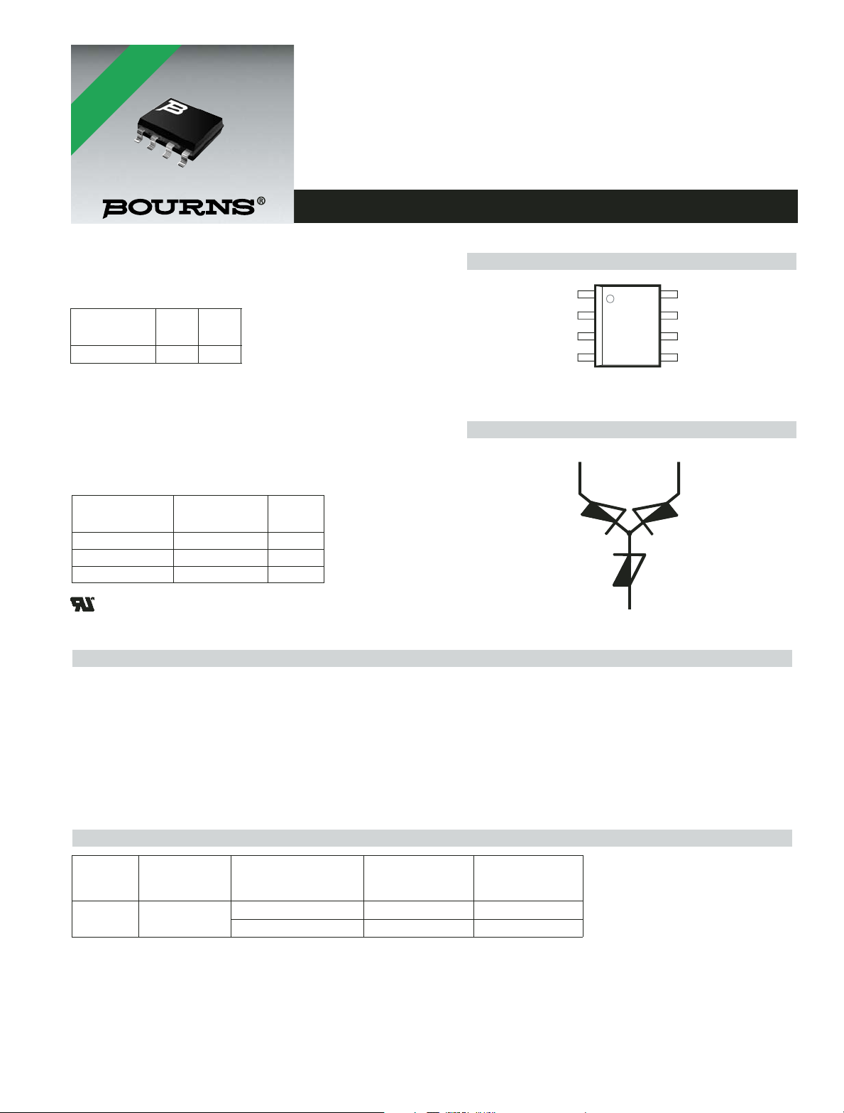
D Package (Top View)
NC
8
7
NC
6
G
NC
MD7XAJA
T2
Device Symbol
1
T1
NC
NC
T2
NC - No internal connection
2
3
45
T1
............................................ UL Recognized Components
SD7XAD
G
Description
The TISP7015 is a 3-point overvoltage protector designed for protecting against metallic (differential mode) and simultaneous longitudinal
(common mode) impulses.
These devices are designed to limit overvoltages between signal, data and control port conductors, connected to terminals T1 and T2, and
a protective ground, G. Each terminal pair has a symmetrical voltage-triggered bidirectional thyristor characteristic (Figure 1). Overvoltages
are initially clipped by breakdown clamping until the voltage rises to the breakover level, which causes the device to crowbar into a
low-voltage on state. This low-voltage on state causes the current resulting from the overvoltage to be safely diverted through the device.
The device switches off when the diverted current falls below the holding current value.
Terminals marked NC do not have any internal connections and may be left floating or tied to some circuit point.
How To Order
Device Package Carrier
TISP7015
D, Small-outline
Embossed Tape Reeled TISP7015DR
For Standard
Termination Finish
Order As
Tube TISP7015D
For Lead Free
Termination Finish
Order As
TISP7015DR-S
TISP7015D-S
*RoHS Directive 2002/95/EC Jan 27 2003 including Annex
JULY 2000 - REVISED FEBRUARY 2005
Specifications are subject to change without notice.
Customers should verify actual device performance in their specific applications.

TISP7015 (VLV) Overvoltage Protector
Absolute Maximum Ratings, TJ = 25 °C (Unless Otherwise Noted)
Rating Symbol Value Unit
Repetitive peak off-state voltage V
Non-repetitive peak on-state pulse current (see Notes 1 and 2)
8/20 (IEC 61000-4-5, clause 7.2, R = 0, combination wave generator) 150
5/310 (ITU-T recommendation K.44, 10/700 generator used for K.20/45/21) 40
10/1000 (Telcordia GR-1089-CORE, 10/1000 voltage wave shape) 30
Non-repetitive peak on-state current (see Notes 1, 2 and 3)
50/60 Hz, 1 s
Junction temperature T
Storage temperature range T
DRM
I
PPSM
I
TSM
stg
± 8V
A
4A
J
-40 to +150 °C
-65 to +150 °C
NOTES: 1. Initially, the TISP7015 must be in thermal equilibrium at the specified T
. The surge may be repeated after the TISP7015
A
returns to its initial conditions.
2. These non-repetitive rated currents are peak values of either polarity.
3. Total return current, I
, value.
G
Electrical Characteristics, TJ = 25 °C (Unless Otherwise Noted)
Parameter Test Conditions Min Typ Max Unit
Repetitive peak off-
I
DRM
state current
V
Breakover voltage dv/dt = ±250 V/ms, R
(BO)
Breakover current dv/dt = ±250 V/ms, R
I
(BO)
V
On-s tate voltage IT = ±5A, tW = 100 µs ±4V
T
Holding current IT = ±5A, di/dt = +/-30 mA/ms ±30 mA
I
H
Off-state current VD = ±0.85V
I
D
C
Off-state capacitance f = 1 MHz, Vd = 30 mV rms, VD = 0 (see Note 4) 32 40 pF
KA
V
= ±V
D
DRM
= 300
= 300
Ω
Ω
SOURCE
SOURCE
, TA = 85 °C ±10 µA
DRM
NOTE 4: Three-terminal guarded measurement, unmeasured terminal voltage bias is zero.
Thermal Characteristics
Parameter Test Conditions Min Typ Max Unit
Junction to free air thermal resistance P
R
θJA
= 0.8 Ω, TA = 25 °C, 5 cm2, FR4 PCB 160 °C/W
tot
±4 µA
±15 V
±100 mA
Customers should verify actual device performance in their specific applications.
Specifications are subject to change without notice.
JULY 2000 - REVISED FEBRUARY 2005
 Loading...