

BOURNS TISP61089B Service Manual
T
N
IA
L
P
S
M
N
E
O
L
IO
C
B
S
S
A
R
H
E
IL
o
V
A
V
*R
A
TISP61089B High Voltage Ringing SLIC Protector
DUAL FORWARD-CONDUCTING P-GATE THYRISTORS
PROGRAMMABLE OVERVOLTAGE PROTECTORS
TISP61089B
Dual Voltage-Programmable Protectors
- Supports Battery Voltages Down to -155 V
- Low 5 mA max. Gate Triggering Current
- High 150 mA min. Holding Current
Rated for LSSGR ‘1089 Conditions
Impulse
Waveshape
2/10
10/360 4.5.7 2, 5 30
10/1000 4.5.7 1,3 30
60 Hz Power
Fault Times
0.5 4.5.12 9 6.5
14.5.123, 4, 8 4.6
24.5.1273.4
5
30 4.5.12 6 1.3
900
‘1089 Test I
Sect ion T es t #
4.5.7
4.5.8
‘1089 Test I
Section Test #
4.5.12
4.5.1352, 3
4.5.12
4.5.13
4.5.15/16
1, 2
1, 4, 5 0.73
TSP
A
4
120
1
TSM
A
2.3
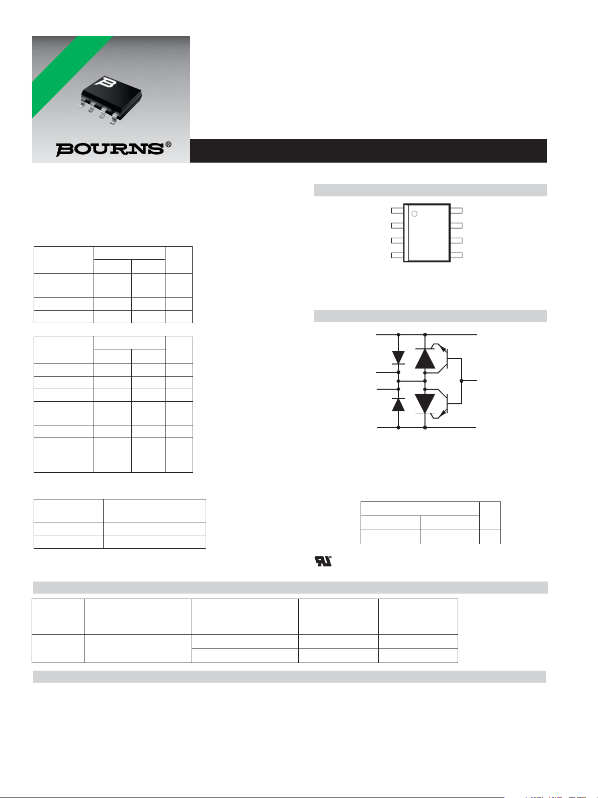
D Package (Top View)
(Tip)
(Gate)
(Ring)
K1
G
NC
K2
1
2
3
4
8
K1
7
A
6
A
5
K2
NC - No internal connection
Terminal typical applica tion name s shown in
parenthesis
Device Symbol
K1
A
A
K2
Te rminals K1, K2 and A correspond to the alternative
line designators of T, R and G or A, B and C. The
negative protection voltage is controlled by the
voltage, V
applied to the G terminal.
GG,
(Tip)
(Ground)
(Ground)
(Ring)
MD6XANB
K1
G
K2
SD6XAEB
2/10 Overshoot Voltage Specified
I
= 100 A, di/dt = 80A/µs
Element
Diode 10
SCR 12
TM
V
Rated for ITU-T K.20, K.21 and K.45
Waveshape
Voltage Curr ent
I
TSP
A
10/700 5/310 40
............................................ UL Recognized Components
How To Order
Device Package Carrier
TISP61089B D (8-pin Small-Outline)
Embossed Tape Reeled TISP61089BDR
For Standard
Te rmination Finish
Order As
Tube TISP61089BD
For Lead Free
Te rmination Finish
Order As
TISP61089BDR-S
TISP61089BD-S
Description
The TISP61089B is a dual forward-conducting buffered p-gate thyristor (SCR) overvoltage protector. It is designed to protect monolithic SLICs
(Subscriber Line Interface Circuits) against overvoltages on the telephone line caused by lightning, a.c. power contact and induction. The
TISP61089B limits voltages that exceed the SLIC supply rail voltage. The TISP61089B parameters are specified to allow equipment
compliance with Bellcore GR-1089-CORE, Issue 2 and ITU-T recommendations K.20, K.21 and K.45.
*RoHS Directive 2002/95/EC Jan 27 2003 including Annex
OCTOBER 2000 - REVISED FEBRUARY 2005
Customers should verify actual device performance in their specific applications.
Specifications are subject to change without notice.

TISP61089B High Voltage Ringing SLIC Protector
Description (Continued)
The SLIC line driver section is typically powered from 0 V (ground) and a negative voltage in the region of -20 V to -150 V. The protector gate is
connected to this negative supply. This references the protection (clipping) voltage to the negative supply voltage. The protection voltage will
then track the negative supply voltage and the overvoltage stress on the SLIC is minimized.
Positive overvoltages are clipped to ground by diode forward conduction. Negative overvoltages are initially clipped close to the SLIC negative
supply rail value. If sufficient current is available from the overvoltage, then the protector SCR will switch into a low voltage on-state condition.
As the overvoltage subsides, the high holding current of TISP61089B SCR prevents d.c. latchup.
The TISP61089B is intended to be used with a series combination of a 40 Ω or higher resistance and a suitable overcurrent protector. Power
fault compliance requires the series overcurrent element to open-circuit or become high impedance (see Applications Information). For
equipment compliant to ITU-T recommendations K.20 or K.21 or K.45 only, the series resistor value is set by the coordination requirements.
For coordination with a 400 V limit GDT, a minimum series resistor value of 10 Ω is recommended.
These monolithic protection devices are fabricated in ion-implanted planar vertical power structures for high reliability and in normal system
operation they are virtually transparent. The TISP61089B buffered gate design reduces the loading on the SLIC supply during overvoltages
caused by power cross and induction. The TISP61089B is available in a 8-pin plastic small-outline surface mount package.
Absolute Maximum Ratings, -40 °C ≤ TJ ≤ 85 °C (Unless Otherwise Noted)
Rating Symbol Value Unit
Repetitive peak off-state voltage, V
Repetitive peak gate-cathode voltage, V
=0 V
GK
=0 V
KA
DRM
GKRM
-170 V
-167 V
Non-repetitive peak on-state pulse current (see Notes 1 and 2)
10/1000 µs(Telcordia (Bellcore) GR-1089-CORE, Issue 2, February 1999, Section 4)
5/320 µs (ITU-T K.20, K.21& K.45, K.44 open-circuit voltage wave shape 10/700 µs)
10/360 µs(Telcordia (Bellcore) GR-1089-CORE, Issue 2, February 1999, Section 4)
I
TSP
30
40
40
A
1.2/50 µs(Telcordia (Bellcore) GR-1089-CORE, Issue 2, February 1999, Section 4) 100
2/10 µs(Telcordia (Bellcore) GR-1089-CORE, Issue 2, February 1999,
Section 4) T
= 25 °C
J
120
170
Non-repetitive peak on-state current, 60 Hz (see Notes 1, 2 and 3)
0.5 s 6.5
1s
2s
I
5s
30 s
900 s
Non-repetitive peak gate current, 1/2 µspulse, cathodes commoned (see Notes 1 and 2) I
Operating free-air temperature range T
Junction temperature T
Storage temperature range T
TSM
GSM
A
J
stg
4.6
3.4
2.3
1.3
0.73
+40 A
-40 to +85 °C
-40 to +150 °C
-40 to +150 °C
A
NOTES: 1. Initially , the protector must be in thermal equilibrium with -40 °C
to its initial conditions.
2. The rated current values may be applied either to the Ring to Ground or to the Tip to Ground term inal pairs. Additionally, both
terminal pairs may have their rated current values applied simultaneously (in this case the Ground terminal current will be twice
the rated current value of an individual terminal pair). Above 85 °C, derate linearly to zero at 150 °C lead temperature.
3. Values f or V
OCTOBER 2000 - REVISED FEBRUARY 2005
Specifications are subject to change without notice.
Customers should verify actual device performance in their specific applications.
= -100 V. For values at other voltages see Figure 2.
GG
T
85 °C. The surge may be repeated after the device returns
≤
≤
J

TISP61089B High Voltage Ringing SLIC Protector
Recommended Operating Conditions
Component Min Typ Max Unit
TISP61089B gate decoupling capacitor 100 220 nF
C
G
TISP61089B series resistor for GR-1089-CORE first-level surge survival 25
TISP61089B series resistor for GR-1089-CORE first-level and second-level surge survival 40 Ω
R
TISP61089B series resistor for GR-1089-CORE intra-building port surge survival 8
S
TISP61089B series resistor for K.20, K.21 and K.45 coordination with a 400 V primary
protector
Electrical Characteristics, TJ = 25 °C (Unless Otherwise Noted)
Parameter Test Condi ti o ns Min Typ Max Unit
V
(BO)
V
GK(BO)
V
V
FRM
I
I
GKS
I
GT
V
C
I
D
Off-state current VD=V
Breakover voltage2/10 µs, ITM=-100 A, di/dt = -80 A/µs, RS=50
Gate-cathode impulse
breakover voltage
F
Forward voltage IF=5A, tw= 200 µs3V
Peak forward recov ery
H
Holding current IT=-1A, di/dt = 1A/ms, VGG=-100 V -150 mA
Gate reverse current VGG=VGK=V
Gate trigger current IT=-3A, t
Gate-cathode trigger
GT
Cathode-anode off-
KA
state capacitance
voltage
voltage
2/10 µs, ITM=-100 A, di/dt = -80 A/µs, RS=50Ω, VGG= -100 V,
(see Note 4)
2/10 µs, I
I
T
f=1MHz, V
DRM
=-3A, t
, VGK=0
= 100 A, di/dt = 80 A/µs, RS=50Ω,(see Note 4) 10 V
F
, VKA=0
GKRM
≥ 20 µs, V
p(g)
≥ 20 µs, V
p(g)
=1V, IG=0, (see Note 5)
d
=-100 V 5 mA
GG
=-100 V 2.5 V
GG
10
T
= 25 °C-5µA
J
= 85 °C-50µA
T
J
VGG=-100 V -112 V
Ω,
12 V
T
= 25 °C-5µA
J
= 85 °C-50µA
T
J
V
=-3V 100 pF
D
V
=-48V 50 pF
D
Ω
Ω
Ω
NOTES: 4. The diode forward recovery and the thyristor gate impulse breakover (overshoot) are not strongly dependent of the gate supply
voltage value (V
GG
).
5. These capacitance measurements employ a three terminal capacitance bridge incor porating a guard circuit. The unmeasured
device terminals are a.c. connected to the guard terminal of the bridge.
Thermal Characteristics
Parameter Test Conditio n s Min Typ Max Unit
T
= 25 °C, EIA/JESD51-3 PCB, EIA/
R
θJA
Junction to free air thermal resistance
A
JESD51-2 environment, P
Customers should verify actual device performance in their specific applications.
TOT
= 1.7 W
OCTOBER 2000 - REVISED FEBRUARY 2005
Specifications are subject to change without notice.
120 °C/W
TISP61089B High Voltage Ringing SLIC Protector
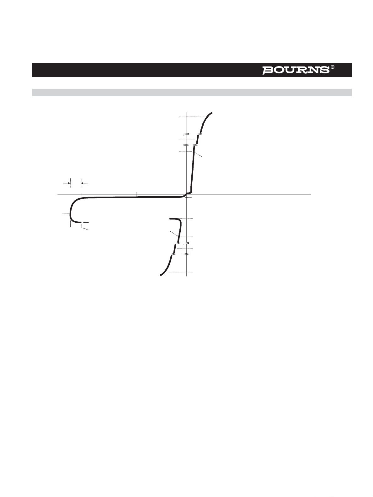
Parameter Measurement Information
-v
I
(BO)
Quadrant III
Switching
Characteristic
+i
I
(= ) |
FSP
TSP
Characteristic
I
(= ) |
FSM
TSM
I
F
V
F
V
GK(BO)
V
GG
I
S
V
(BO)
V
S
V
D
I
D
I
H
V
T
I
T
I
TSM
I
TSP
-i
Quadrant I
Forwar d
Conduction
+v
PM6XAAA
Figure 1. Voltage-Current Characteristic
Unless Otherwise Noted, All Voltages are Referenced to the Anode
OCTOBER 2000 - REVISED FEBRUARY 2005
Specifications are subject to change without notice.
Customers should verify actual device performance in their specific applications.

TISP61089B High Voltage Ringing SLIC Protector
Thermal Information
PEAK NON-RECURRING AC
vs
20
15
10
8
7
6
5
4
3
2
1.5
1
0.8
— Peak Non-Recurrent 50 Hz Curr ent — A
0.7
TSM
I
0.6
0.5
0.01 0.1 1 10 100 1000
t — Current Duration — s
Figure 2. Non-Repetitive Peak On-State Current against
RING AND TIP TERMINALS:
Equal I
values applie d
TSM
simultaneously
GROUND TERMINAL:
Current twice I
TSM
EIA /JES D51
Environm ent and
PCB, T
VGG = -80 V
VGG = -100 V
VGG = -120 V
Duration
CURRENT DURATION
TI61AF
value
= 25 °C
A
VGG = -60 V
TYPICAL PEAK NON-RECURRING AC
vs
CURRENT DURATION
20
15
10
8
7
6
5
4
3
2
1.5
1
0.8
— Peak Non-Recurrent 50 Hz Current — A
0.7
TSM
I
0.6
0.5
0.01 0.1 1 10 100 1000
t — Current Duration — s
Figure 3. Typical No n-Repetitive Peak On-state Current
RING AND TIP TERMINALS:
Equal I
values appl ied
TSM
simultaneously
GROUND TERMINAL:
Current twice I
V
VGG = -100 V
VGG = -120 V
against Duration
value
TSM
Typical PCB
Mounting,
T
= 25 °C
A
= -80 V
GG
TI61DA
VGG = -60 V
OCTOBER 2000 - REVISED FEBRUARY 2005
Customers should verify actual device performance in their specific applications.
Specifications are subject to change without notice.

TISP61089B High Voltage Ringing SLIC Protector
APPLICATIONS INFORMATION
Operation of Ringing SLICs using Multiple Negative Voltage Supply Rails
Figure 4 shows a typical powering arrangement for a multi-supply rail SLIC. V
switch S1 in the position shown, the line driver amplifiers are powered between 0 V and V
for short loop transmission. For long loops and to generate ringing, the driver voltage is increased by operating S1 to connect V
is a lower (smaller) voltage supply than V
BATL
. This mode minimizes the power consumption
BATL
BATH
conditions are shown in Figure 5.
SLIC
0 V
. With supply
. These
BATH
LINE
LINE
DRIVERS
Figure 4. SLIC with Voltage Supply Switching
0 V 0 V
V
BATL
S1
SUPPL Y
SWITCH
V
DCRING
V
PKRING
V
PKRING
V
BATL
V
BATH
AI6XCC
/2
/2
V
SLICG
V
PKRING
V
PKRING
0 V
/2
V
BATH
/2
V
SLICH
SHORT LOOP
LONG LOOP
V
BATH
RINGING
AI6XCD
V
BATH
Figure 5. Driver Supply Voltage Levels
Conventional ringing is typically unbalanced ground or battery backed. To minimize the supply voltage required, most multi-rail SLICs use
balanced ringing as shown in Figure 5. The ringing has d.c., V
has a peak value, V
internal losses in the SLIC from ground, V
10 V. This makes a total, V
, of 99 V. If the d.c. component was 20 V, then the total voltage swing needed would be 99 + 20 = 119 V. There are
PKRING
, supply rail value of 119 + 10 = 129 V.
BATH
, and the negative supply, V
SLICG
In some cases a trapezoidal a.c. ring signal is used. This would have a peak to r.m.s ratio (crest factor) of about 1.25, increasing the r.m.s. a.c.
ring level by 13 %. The d.c. ring voltage may be lowered for short loop applications.
OCTOBER 2000 - REVISED FEBRUARY 2005
Specifications are subject to change without notice.
Customers should verify actual device performance in their specific applications.
DCRING
, and a.c., V
SLICH
, components. A 70 V r.m.s. a.c. sinusoidal ring signal
PKRING
. The sum of these two losses generally amounts to a total of

TISP61089B High Voltage Ringing SLIC Protector
SLIC Parameter Values
The table below shows some details of HV SLICs using multiple negative supply rails.
Manufacturer INFINEON‡ LEGERITY™‡
SLIC Series SLIC-P‡ ISLIC™‡
SLIC # PEB 4266 79R241 79R101 79R100
Data Sheet Issue 14/02/2001 -/08/2000 -/07/2000 -/07/2000
Short Circuit Current 110 150 150 150 mA
max. -155 -104 -104 -104 V
V
BA TH
max. -150 -104 V
V
BATL
AC Ri nging for: 85 45† 50† 55† V rms
Crest Factor 1.4 1.4 1.4 1.25
V
BATH
V
BA TR
R or T Power Max. < 10 ms 10 W
R or T Overshoot < 10 ms TBD T BD -5 5 -10 5 - 10 5 V
R or T Overshoot < 1 ms -10 +10 V
R or T Overshoot < 1 µs -10 +30 -10 10 -15 8 -15 8 V
R or T Overshoot < 250 ns -15 15 -20 12 -20 12 V
Line Feed Resistance 20 + 30 50 50 50
† Assumes -20 V battery voltage during ringing.
‡ Legerity, the Legerity logo and ISLIC are the trademarks of Legerity, Inc. (formerly AMD’s Communication Products Division).
Other product names used in this publication are for identification purposes only and may be trademarks of their respective
companies.
From the table, the maximum supply voltage, V
1 µs and -15 V, +12 V are needed for 250 ns. To maintain these voltage limits over the temperature range, 25 °C values of -12 V, +10 V are
needed for 250 ns.
-70 -90 -99 -99 V
-150 -36 -24 -24 V
, is -155 V. In terms of minimum voltage overshoot limits, -10 V and +8 V are needed for
BATH
BATH
V
BA TH
Unit
V
Ω
It is important to define the protector overshoot under the actual circuit current conditions. For example, if the series line feed resistor was
40 Ω, R1 in Figure 12, and Telcordia GR-1089-CORE 2/10 and 10/1000 first-level impulses were applied, the peak protector currents would be
56 A and 20 A. At the second-level, the 2/10 impulse current would be 100 A. Therefore, the protector voltage overshoot should be guaranteed
to not exceed the SLIC voltage ratings at 100 A, 2/10 and 20 A, 10/1000. In practice, as the 2/10 waveshape has the highest current (100 A)
and fastest di/dt (80 A/µs) the overshoot level testing can restricted to the be 2/10 waveshape.
Using the table values for maximum battery voltage and minimum overshoot gives a protection device requirement of -170 V and +12 V from
the output to ground. There needs to be temperature guard banding for the change in protector characteristics with temperature. To cover
down to -40 °C, the 25 °C protector minimum values become -185 V (V
) on the cathode and -182 V (V
DRM
) on the gate.
GKS
Gated Protectors
This section covers four topics. First, it is explained why gated protectors are needed. Second, the voltage limiting action of the protector is
described. Third, how the withstand voltages of the TISP61089B junctions are set. Fourth, an example application circuit is described.
Purpose of Gated Protectors
Fixed voltage thyristor overvoltage protectors have been used since the early 1980s to protect monolithic SLICs (Subscriber Line Interface
Circuits) against overvoltages on the telephone line caused by lightning, a.c. power contact and induction. As the SLIC was usually powered
from a fixed voltage negative supply rail, the limiting voltage of the protector could also be a fixed value. The TISP1072F3 is a typical example
of a fixed voltage SLIC protector.
OCTOBER 2000 - REVISED FEBRUARY 2005
Customers should verify actual device performance in their specific applications.
Specifications are subject to change without notice.
 Loading...