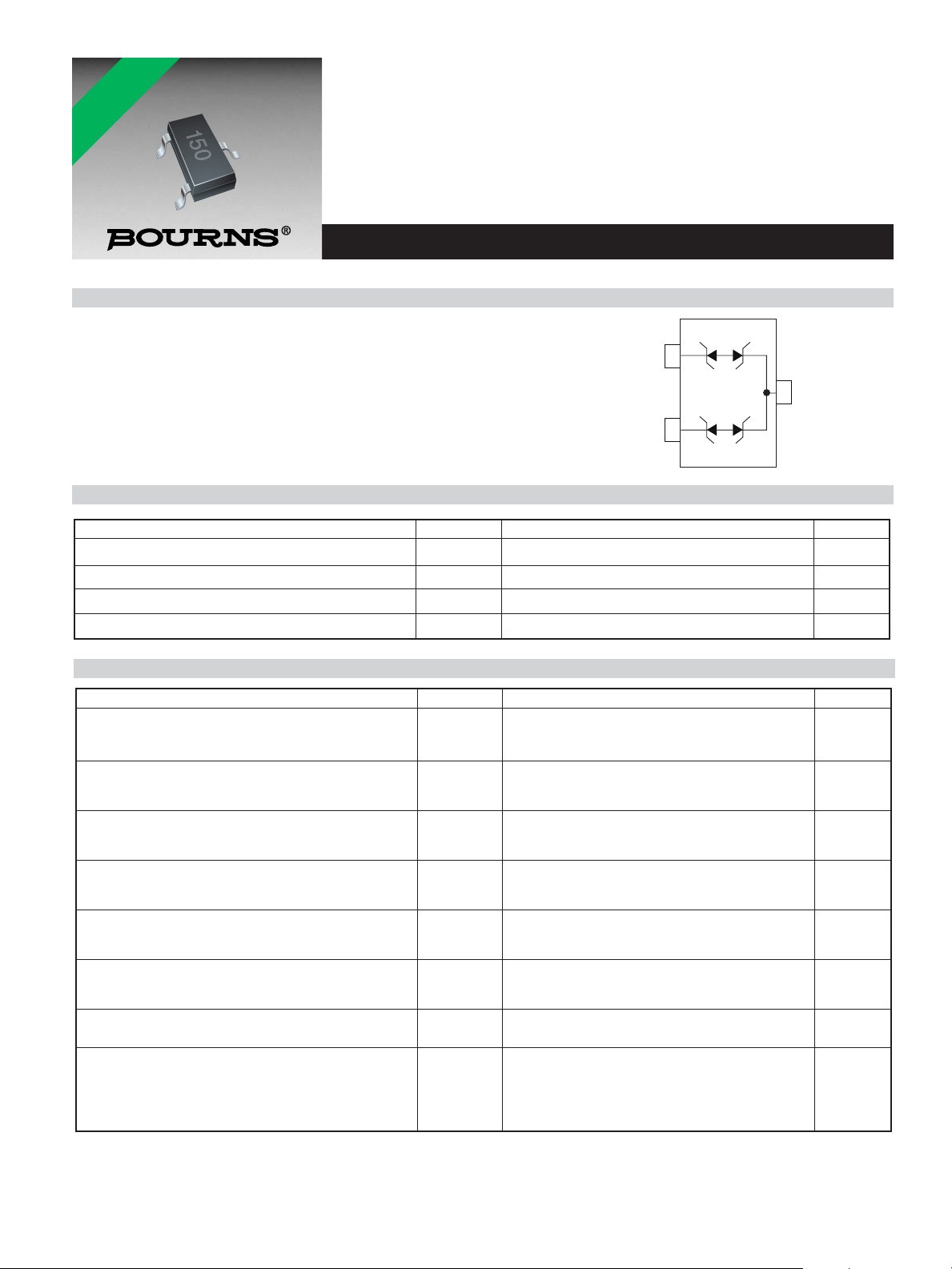
Bourns CDSOT23-SM712 Schematic [ru]

CDSOT23-SM712 — Surface Mount TVS Diode
Features
RoHS compliant*
Working peak voltage 7 V or 12 V
ESD protection 30 kV max.
Surge protection
Applications
Wireless systems
Network protection
Portable electronics
RS485 port protection
General Information
Absolute Maximum Ratings (@ TA= 25 °C Unless Otherwise Noted)
The CDSOT23-SM712 device provides ESD, EFT and Surge protection for data ports
meeting IEC 61000-4-2 (ESD), IEC 61000-4-4 (EFT) and IEC 61000-4-5 (Surge)
requirements. The Transient Voltage Suppressor array offers 2 TVS diodes with
Working Peak Reverse Voltage of 7 V or 12 V with Minimum Breakdown Voltage of
7.5 V or 13.3 V respectively.
The SOT23 packaged device will mount directly onto the industry standard SOT23
footprint. Bourns®Chip Diodes conform to JEDEC standards, are easy to handle with
standard pick and place equipment and the flat configuration minimizes roll away.
*RoHS COMPLIANT
*RoHS Directive 2002/95/EC Jan. 27, 2003 including annex and RoHS Recast 2011/65/EU June 8, 2011.
Specifications are subject to change without notice.
Customers should verify actual device performance in their specific applications.
Parameter Symbol Value Unit
Peak Pulse Power (tp= 8/20 µs)
1
P
PK
400 W
Peak Pulse Current (8/20 µs) I
PP
17 A
Storage Temperature T
STG -55 to +150
°C
Operating Temperature T
OPR -55 to +150
°C
Electrical Characteristics (@ TA= 25 °C Unless Otherwise Noted)
Note:
1. See Peak Pulse Power vs. Pulse Time.
Parameter Symbol Value Unit
Minimum Breakdown Voltage @ 1 mA
Pin 3 - 1 and Pin 3 - 2 V
BR
7.5 V
Pin 1 - 3 and Pin 2 - 3 13.3
Maximum Working Peak Voltage
Pin 3 - 1 and Pin 3 - 2 V
WM
7.0 V
Pin 1 - 3 and Pin 2 - 3 12.0
Maximum Leakage Current @ V
WM
Pin 3 - 1 and Pin 3 - 2 I
D
20.0 µA
Pin 1 - 3 and Pin 2 - 3 1.0
Maximum Clamping Voltage @ IP= 1 A
Pin 3 - 1 and Pin 3 - 2 V
C
11 V
Pin 1 - 3 and Pin 2 - 3 19
Maximum Clamping Voltage @ IP= 5 A
Pin 3 - 1 and Pin 3 - 2 V
C
12 V
Pin 1 - 3 and Pin 2 - 3 20
Maximum Clamping Voltage @ IPP= 17 A
Pin 3 - 1 and Pin 3 - 2 V
C
14 V
Pin 1 - 3 and Pin 2 - 3 26
Typical Junction Capacitance @ 0 V, 1 MHz
(Pin 3-1 and Pin 3-2) & (Pin 1 - 3 and Pin 2 - 3) C
D
75 pF
ESD Protection (per IEC 61000-4-2)
Contact - Min. ±8
Contact - Max. ESD ±30 kV
Air - Min. ±15
Air - Max. ±30
1
3
2

CDSOT23-SM712 — Surface Mount TVS Diode
Specifications are subject to change without notice.
Customers should verify actual device performance in their specific applications.
1
2
3
B
CD
H
L
0 ° TO 8 °
I
GAUGE
PLANE
K
J
SEATING PLANE
SEE
DETAIL
A
DETAIL
A
G
E
F
A
Dimensions
A
2.80 - 3.00
(0.110 - 0.118)
B
0.95
(0.037)
C
1.20 - 1.40
(0.047 - 0.055)
D
2.10 - 2.49
(0.083 - 0.098)
E
1.90
(0.075)
F
0.30 - 0.50
(0.012 - 0.019)
G
0.89 - 1.17
(0.035 - 0.046)
H
0.05 - 0.015
(0.002 - 0.006)
I
0.25
(0.010)
J
0.46 - 0.64
(0.018 - 0.025)
K
0.40 - 0.58
(0.016 - 0.023)
L
0.08 - 0.20
(0.003 - 0.008)
Dimensions
A
0.95
(0.037)
B
0.95
(0.037)
C
2.00
(0.079)
D
0.85
(0.033)
E
0.85
(0.033)
This is a molded JEDEC SOT-23 package with 100 % Matte Sn
plating on the lead frame. It weighs approximately 8 mg and has a
flammability rating of UL 94V-0.
Recommended Footprint
How To Order
CD SOT23 - SM 712
Common Code
Chip Diode
Package
• SOT23 = SOT23 Package
Model
SM = Special Model
Working Peak Reverse Voltage
712 = 7 V
RWM & 12 VRWM (Volts)
Product Dimensions
CDSOT23-SM712 ...................................................................... 712
Typical Part Marking
BSC
BSC
BSC
MILLIMETERS
(INCHES)
DIMENSIONS =
A B
C
E
D
DIMENSIONS =
MILLIMETERS
(INCHES)
 Loading...