

Page 1

DR-770 Feb. 1999
SERVICE NOTES
First Edition
Issued by RJA
Dr. Rhythm
TABLE OF CONTENTS Page
SPECIFICATIONS ............................................................................................... 1
Deterioration in the conductive coating inside the case ............................................................................................... 2
PANEL LAYOUT ............................................................................................... 2
EXPLODED VIEW ............................................................................................... 3
PARTS LIST ............................................................................................... 4
LOADING THE FACTORY PRESET DATA ............................................................................................... 6
IDENTIFYING THE VERSION NUMBER ............................................................................................... 6
USER DATA SAVE AND LOAD ............................................................................................... 6
How to save the User Data ............................................................................................... 6
How to load the User Data ............................................................................................... 7
TEST MODE ............................................................................................... 8
TROUBLESHOOTING ............................................................................................... 11
ERROR MESSAGE ............................................................................................... 12
BLOCK DIAGRAM ............................................................................................... 13
CIRCUIT DIAGRAM (JACK) ............................................................................................... 14
CIRCUIT BOARD (JACK) ............................................................................................... 15
CIRCUIT DIAGRAM (MAIN) ............................................................................................... 16
CIRCUIT BOARD (MAIN) ............................................................................................... 17
Change Information ............................................................................................... 18
目次
主な仕様
ケース内側の導電塗装の劣化について
パネル配置図
分解図
パーツリスト
ファクトリー・プリセット・データのロードの方法
バージョンの確認方法
データのセーブとロードの方法
ユーザーデータのセーブ方法
ユーザーデータのロード方法
テストモード
トラブルシューティング
エラー・メッセージ
ブロック図
回路図(JACK)
基板図(JACK)
回路図(MAIN)
基板図(MAIN)
変更案内
SPECIFICATIONS
● Instruments
255
● Maximum Polyphony
14 voices
● Rhythm Patterns
Preset Patterns : 400
User Patterns : 400
● Song
Songs :100
Song Length : Maximum 250 parts for a song
Total Parts for Songs : 10,000
● Effect
Reverb,Flanger
● Resolution
Per quarter note : 96
● Tempo
Quarter note=20 ~ 260
● Data Input Method
Realtime/Step
● Maximum Note Storage
approx.11,200note
● Output Level
Max.7 Vp-p(L(MONO),R)
● Noise Level
Less Than -78 dBm(DIN AUDIO)((L(MONO))
● Output Impedance
1kΩ(L(MONO),R, INDIVIDUAL))
● Power Source
AC Adaptor BOSS BRC Series
● Current Draw
700mA
主な仕様
● 音色数
255
● 最大同時発音数
14 voices
● リズムパターン数
プリセットパターン :400
ユーザーパターン :400
● ソング
ソング数 :100
ソング長 :1ソング当たり最大250パターン
総ソング長 :10,000
● エフェクト
リバーブ、フランジャー
● 分解能
4分音符当り:96
● テンポ
Quarternote/4分音符=20〜260
● データ入力方式
リアルタイム、ステップ
●最大記憶音数
約11,200音
●出力レベル
最大7Vp-p(L(MONO),R)
●ノイズレベル
-78dBm以下(DINAUDIO)((L(MONO))
● 出力インピーダンス
1kΩ(L(MONO),R, INDIVIDUAL))
●電源
ACアダプターBOSSBRCシリーズ
● 消費電流
700mA
● Dimensions
215(W)×165(D)×57(H)mm
8-1/2(W)×6-1/2(D)×2-3/8(H)inches
● Weight
715g/1 lbs 10 oz
● Accessories
Owner's Manual Set(English) : PNo.71238223
Owner's Manual Set(Japanese) : PNo.71238145
AC Adaptor
AC ADAPTOR BRC-100 BOSS :PNo.00899078
AC ADAPTOR BRC-120 BOSS :PNo.00899089
AC ADAPTOR BRC-230 BOSS :PNo. 00899090
AC ADAPTOR BRC-240A BOSS :PNo. 00899101
EURO CONVERTER PLUG ECP01-5A :PNo. 00905234
● 外形寸法
215(W)×165(D)×57(H)mm
8-1/2(W)×6-1/2(D)×2-3/8(H)inches
●重量
715g/1lbs10oz
● 標準付属品
取扱説明書(和文) :PNo.71238145
取扱説明書(英文) :PNo.71238223
保証書(JapanOnly) :PNo.40232334
ACAdaptor
ACADAPTORBRC-100BOSS:PNo.00899078
Copyright © 1999 by ROLAND CORPORATION
All rights reserved. No part of this publication may be reproduced in any form without the written permission of ROLAND CORPORATION.
本書の一部、もくしは全部を無断で複写・転載することを禁じます。
17059959 Printed in Japan AA00 (DP)
1
Page 2
DR-770 Feb. 1999
Top Case
(01787767)
LED (red)
SLC-22VR3F
15039221
LED (green)
SLC-22MG3F
15039222
Rubber Switch KEY
(01787790)
Rubber Switch PAD
(01787801)
Pressure Sheet Sensor
(25095101)
Plate
(22055165)
<Top View>
Display Cover
(01787778)
LCD
RCD1627R
(01788490)
DR-Knob (BLK)
(22485303)
Rotary Volume
RK14k 124 50KB×2
(13289189)
DR-Knob (BLK)
(22485303)
Rotary Encoder
EC16B 24204
(01231367)
KEY Top
(12499175)
Switch
SPUN19F
(13129369)
Jack
HEC0740-01-010
(13449728)
Jack
YKB21-5130
(13449433)
Jack
HLJ7101-01-3010
(13449283)
Bottom Case
(01787734)
Jack
HLJ7001-01-3010
(13449284)
MIDI Connector
M-S2-3P
(13429642)
■
Deterioration in the conductive
coating inside the case
The inside of the case is coated with a conductive material. If the
board undergoes repeated detaching/attaching, the coating on the
boss may deteriorate.
If the resistance value between the case center and the head of the
boss becomes 5Ω or more, the effect of conductive coating cannot
be expected. In such a case, replace the case.
ケース内側の導電塗装の劣化に
ついて
ケース内側には導電塗装が施されていますが、基板の取り外
し、取り付けを繰り返すと、ボスの部分の塗装が劣化してき
ます。
ケース中心とボスの頭との抵抗値が、5Ω以上になると、導電
塗装の効果が望めなくなりますので、ケースを交換して下さ
い。
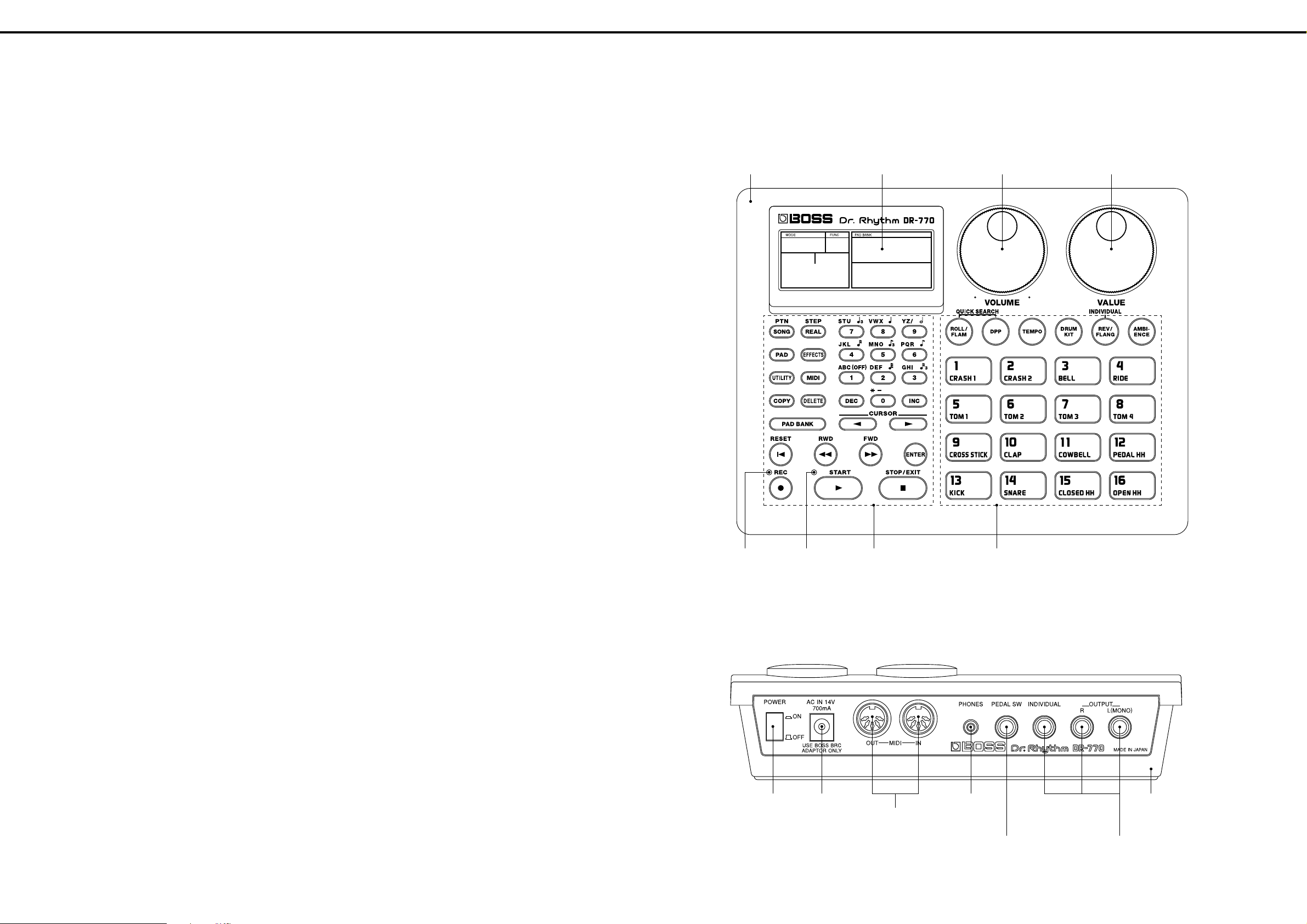
PANEL LAYOUT
FRONT VIEW
/正面図
/パネル配置図■
REAR VIEW
/背面図
2
Page 3
DR-770 Feb. 1999
A
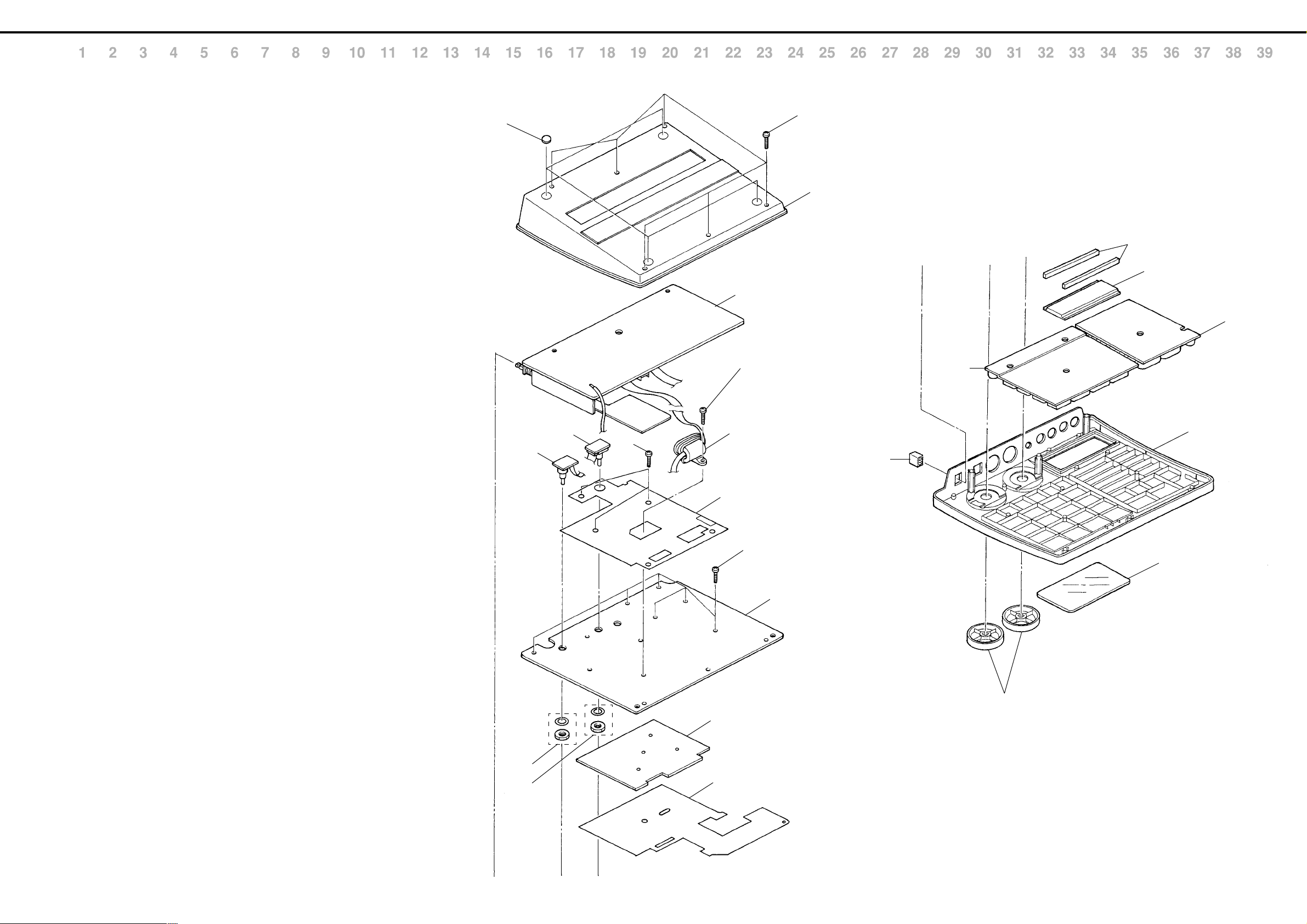
EXPLODED VIEW
[Part]
NO.
B
C
D
E
F
G
H
I
J
[Screw]
PART CODE
q 01787734 BOTTOM CASE
w 01898189 FOOT D10 T4
e 71238156 JACK BOARD ASSY
r 12449445 FERRITE-CORE ESD-R-16C
t 71238167 VR BOARD ASSY
y 71238178 ENC BOARD ASSY
u 01892034 VR SHIELD SHEET
i 71238123 MAIN BOARD ASSY (EXG)
o 22055165 PLATE 205-165
!0 25095101 PRESSURE SHEET SENSOR 509-101
!1 23365653 RUBBER CONNECTOR 336-653
!2 01788490 LCD RCD1627R
!3 01787790 RUBBER SW KEY
!4 01787801 RUBBER SW PAD
!5 01787767 TOP CASE
!6 12499175 G S-BUTTON S1H BLK 249-175
!7 01787778 DISPLAY COVER
!8 22485303 D R-KNOB L BLK 248-303
NO.
PART CODE
a 40012456 SCREW M2.6×8 BINDING TAPTITE P FE NI
b 40012489 SCREW M2.6×10 BINDING TAPTITE FE BZC
c 40011223 SCREW M2.6×6 BINDING TAPTITE P NI
K
d
d このワッシャーとナットは、#01231367ROTARYENCODERに含まれます。
This MG WASHER and MG NUT are included in the #01231367 ROTARY ENCODER.
L
e このワッシャーとナットは、#13289189POTENTIOMETERに含まれます。
This MG WASHER and MG NUT are included in the #13289189 POTENTIOMETER.
PART NAME DESCRIPTION
PART NAME DESCRIPTION
/分解図
2
6
5
c
7
4
3
b
a
1
!1
!2
!3
!4
!5
!6
M
N
O
P
Q
R
S
T
U
d
e
c
!7
8
!8
9
!0
V
3
Page 4
DR-770 Feb. 1999
PARTS LIST
SAFETY PRECAUTION:*1
The parts marked
related characteristics.
Use only listed parts for
replacement.
安全上の注意:*1
が付いている部品は、安全
上特別な規格でつくられたも
のです。
交換の際は、指定された部品
番号以外の部品は使わないよ
うにして下さい。
Note : Consider about the natural environment carefully before through the old lithium battery away when you exchange to the new one.you exchange to the new one.
注意 : リチウム電池の交換時に、不要になったリチウム電池は、環境問題を十分考慮した上で処理して下さい。
have safety-
/パーツリスト
The parts marked #
are new (initial
parts). *2
#の付いた部品は新
規部品です。*2
CONSIDERATIONS ON PARTS ORDERING
When ordering any parts listed in the parts list, please specify the following items in the order sheet.
Failure to completely fill the above items with correct number and description will result in delayed or even
undelivered replacement.
パーツ発注に関するお願い
オーダーシートには、必ず下記の4項目は正確に記入して下さい。(例外は除く)
もし記入洩れ、誤記等が有る場合、必要部品が発送できなかったり、大幅な遅れの原因になりま
す。御協力をお願いします。
QTY PART NUMBER DESCRIPTION MODEL NUMBER
10 22575241 Sharp key C-20/50
Ex.
15 2247017300 Knob (orange) DAC-15D
必要数 パーツナンバー 品名 使用機種
10 22575241 Sharp key C-20/50
例)
15 2247017300 Knob (orange) DAC-15D
MB → Main Board Assy
VB → VR Board Assy
EB → ENC Board Assy
JB → Jack Board Assy
*1 *2
↓↓ CASING Q'ty
/ケース
# 01787734 BOTTOM CASE 1
# 01787767 TOP CASE 1
# 01787778 DISPLAY COVER 1
22055165 PLATE 205-165 1
KNOB, BUTTON
/つまみ、ボタン
12499175 G S-BUTTON S1H BLK 249-175 1
22485303 D R-KNOB L BLK 248-303 2
# 01787790 RUBBER SW KEY 1
# 01787801 RUBBER SW PAD 1
SWITCH
/スイッチ
13129369 SPUN19430A PUSH SWITCH SW101 on JB 1
JACK, SOCKET
/ジャック、ソケット
13429642 M-S2-3P MIDI SOCKET JK108,JK107 on JB 2
13449433 3.5MM STEREO YKB21-5130 JACK JK105 on JB 1
13449283 6.5MM HLJ7101-01-3010 JACK JK102,JK103,JK104 on JB 3
13449284 6.5MM HLJ7001-01-3010 JACK JK101 on JB 1
13449728 HEC0740-010010 ADAPTOR JACK JK106 on JB 1
DISPLAY UNIT
/表示ユニット
# 01788490 RCD1627R LCD 1
PCB ASSY
/基板完成品
# E 71238123 MAIN BOARD ASSY (EXG) 1
NOTE : 'MAIN BOARD ASSY' includes the following parts.
注意 :補修用MAINBOARDASSYは、下記の部品を含みます。
12169388 LED SPACER LH-3-3 2
# 71238178 ENC BOARD ASSY 1
NOTE : 'ENC BOARD ASSY' includes the following parts.
注意 :補修用ENCBOARDASSYは、下記の部品を含みます。
23505274 WIRING HARNESS B 3P 350-274 1
# 71238156 JACK BOARD ASSY 1
NOTE : 'JACK BOARD ASSY' includes the following parts.
注意 :補修用JACKBOARDASSYは、下記の部品を含みます。
# 01898889 WIRING GND 1P 1
# 01788556 WIRING 6P 1
# 01898989 WIRING W11 1
# 01898001 HEATSINK (DR-770) 1
22465939 HEATSINK (DR-660) 1
22190758 HOLDER DIN SOCKET (2P) 1
40011112 SCREW M3¥10 BINDING TAPTITE B BZC 2
40011090 SCREW M3¥6 BINDING TAPTITE B BZC 2
40016512 LOCKING TIE 80M/M T-18S 2
40016545 INSULOK TIE SKM-1 1
# 71238167 VR BOARD ASSY 1
NOTE : 'VR BOARD ASSY' includes the following parts.
注意 :補修用VRBOARDASSYは、下記の部品を含みます。
23505275 WIRING HARNESS C 6P 350-275 1
IC
# 01784678 HD6415108RF12 IC (CPU) IC6 on MB 1
15199923 SED1278F0A IC (LCD DRIVER) IC9 on MB 1
15239197 MB622928PF-G-BND-ER IC (GATE ARRAY) IC19 on MB 1
15239229 TC6116AF (GP-4) IC (PCM CUSTOM) IC5 on MB 1
01560289 TC55257DFL-55L(EL) IC SRAM IC10 on MB 1
01122412 TC551001CF-70L IC (SRAM) IC12 on MB 1
# 01788589 LHMN4708 IC (MASK ROM) IC8 on MB 1
# 01788578 LHMN5KRP WAVE ROM IC (MASK ROM) IC4 on MB 1
01340789 BU9480F IC (D/A CONVERTER) IC15,IC16 on MB 2
15259864T0 TC74HC4052AF(EL) IC IC13,IC11 on MB 2
15249104 TC7S04F(TE85L) IC (C MOS) IC14 on MB 1
15249111 TC7WU04F(TE12L) IC (C MOS) IC3 on MB 1
15259889 TC7S02F(TE85L) IC IC18 on MB 1
15269805 TC74AC14F(EL) IC IC2 on MB 1
15269810 TC74AC138F(EL) IC (CMOS) IC17 on MB 1
15289131 BA10393F-E2 IC (COMPARATOR) IC1 on MB 1
15289709 M51954BFP-600D IC (RESET) IC20 on MB 1
15289125 PC-410KT 178FAY IC (PHOTO COUPLER) IC7 on MB 1
15189186 UPC4570C IC (OP AMP) BIPOLAR IC102,IC101 on JB 2
15189248 M5216P IC (OP AMP) BIPOLAR IC103 on JB 1
# 01784834 M62421SP FILTER IC106 on JB 1
# 01897801 UPC7805AHF IC (REGULATOR) IC104 on JB 1
# 01897223 UPC24M09AHF IC (REGULATOR) IC105 on JB 1
TRANSISTOR
/トランジスター
15309101 2SA1037KR T146 QRS TRANSISTOR Q3 on MB 1
15329518 DTA114TKT146 TRANSISTOR Q2,Q1 on MB 2
# 00894489 2SA1049-GR(TPE4) TRANSISTOR Q104 on JB 1
# 01788734 2SC2459-GR(TPE4) TRANSISTOR Q106,Q105 on JB 2
15129204 DTC343TS TP TRANSISTOR Q101,Q102,Q103 on JB 3
4
Page 5
DR-770 Feb. 1999
DIODE
/ダイオード
15339135T0 1SS300(TE85R) DIODE DA2-DA20 on MB 19
01127489 RB715F T106 SCHOTTKY DIODE DA1 on MB 1
# 15039221 SLC-22VR3F LED LED1 on MB 1
# 15039222 SLC-22MG3F LED LED2 on MB 1
15019126 1SS133 T-77 SWITCHING DIODE D104,D105,D106,D107 on JB 4
15019260 1G4B42 1A/400V BRIDGE DIODE D102 on JB 1
01122323 MTZJ T-77 8.2B ZENER DIODE D101 on JB 1
01122312 MTZJ T-77 5.6C ZENER DIODE D103 on JB 1
RESISTOR
15399975 RCE9A223JA (22KOHM X8) RESISTOR ARRAY RA4 on MB
15409113 EXBV8V103JV RESISTOR ARRAY RA7 on MB 1
15399965 RCE9A103JAG7A (10KOHM X8) RESISTOR ARRAY RA1,RA2,RA3 on MB
# 01788489 CNB2B9ZTE332 J R-ARRAY RA5,RA6 on MB 2
# 13749187 SR50TR 220 J CARBON RESISTOR R127,R132 on JB 2
# 01897834 ERF5AJ 150 CEMENT RESISTOR R137 on JB 1
# 01897812 RSSX3 5.6 OHM J MTL.OXIDE RESISTOR R136 on JB
POTENTIOMETER
13289189 RK14K124 L1=15 50KBX2 POTENTIOMETER VR301 on VB 1
CAPACITOR
# 00783990 MMTVA0050J474 200 M.POLYEST CAP. C150,C151 on JB 2
# 01897778 16MV470CZ CHEMICAL CAPACITOR C154 on JB 1
# 01897789 25MV470CZ+T CHEMICAL CAPACITOR C136,C137 on JB 2
# 01897790 16MV100UGX+T CHEMICAL CAPACITOR C142 on JB 1
# 01897945 35MV10UGX CHEMICAL CAPACITOR C163 on JB 1
/抵抗
/ボリューム
/コンデンサー
MISCELLANEOUS
12569249S0 LITHIUM BATTERY CR2032 220MAH/3V 1
# 01898189 FOOT D10 T4 4
25095101 PRESSURE SHEET SENSOR 509-101 1
# 01892034 VR SHIELD SHEET 1
13429566 IC SOCKET 400-032-001 32P 1
12569420 LITHIUM BATTERY HOLDER (HL32-A2) FOR CR2032 1
ACCESSORIES (STANDARD)
00899078 AC ADAPTOR BRC-100 1
00899089 AC ADAPTOR BRC-120 1
00899090 AC ADAPTOR BRC-230 1
00899101 AC ADAPTOR BRC-240A 1
00905234 EURO CONVERTER PLUG ECP01-5A (PLUG FOR BRC-230T) 1
# 71238145 OWNER'S MANUAL JAPANESE 1
# 71238223 OWNER'S MANUAL ENGLISH 1
40232334 保証書 (JAPAN ONLY)
/その他
/標準付属品
INDUCTOR, COIL, FILTER
12449370 SBT-0160W EMI FILTER L117 on JB 1
12449381 SBT-0460TF (TP) EMI FILTER L101-L111 on JB 11
12449445 ESD-R-16C FERRITE-CORE 1
CRYSTAL, RESONATOR
00891801 MA-406 24.000MHZ CRYSTAL X1 on MB 1
ENCODER
01231367 EC16B24204 (L=15) ROTARY ENCODER on EB 1
CONNECTOR
23365653 336-653 RUBBER CONNECTOR 2
13369874 IL-Z-11PL-SMTY-E1500 CONNECTOR CN2 on MB 1
13369928 53253-0610 CONNECTOR CN1 on MB 1
13369968 IL-404-17S-LW CONNECTOR CN3 on MB 1
13369942 53254-0610 CONNECTOR CN101 on JB 1
13369939 53254-0310 CONNECTOR CN103 on JB 1
SCREW
40012489 SCREW M2.6×10 BINDING TAPTITE FE BZC 1
40011223 SCREW M2.6×6 BINDING TAPTITE P NI 9
40012456 SCREW M2.6×8 BINDING TAPTITE P FE NI 6
PACKING
# 01897923 PAD ADAPTOR 1
# 01788512 PAD UPPER 1
# 01788523 PAD LOWER 1
# 01788501 PACKING CASE 1
/エンコーダー
/コネクター
/ねじ類
/梱包材
/インダクター、コイル、フィルター
/クリスタル、発振子
5
Page 6
DR-770 Feb. 1999
FUNCMODE
INSERT
COPY
DELETE
SONG
PATTERN
PAD
UTILITY
REAL
STEP
EFFECTS
MIDI
QUANTIZE
NEXT PTN
PART
BEAT
LENGTH
PATTERN
Data to be transferred
転送するデータ
LOADING THE FACTORY
PRESET DATA
1. Turn off the power to the DR-770.
2. While simultaneously pressing the [RESET] and [REC] buttons
turn the power on.
3. The display will show “INIT?”.
4. Press the [ENTER] button and the display will show “SURE?”.
NOTE : If initialization is not necessary do not press the [ENTER]
button.
Press the [STOP/EXIT] button. The display will show “Aborted”
and the operation will enter normal mode.
5. Press the [ENTER] button again. The DR-770 is loaded the
Factory preset Data and then the display will show “Done” and
the operation will enter normal mode.
ファクトリー・プリセット・データ
のロードの方法
1. DR-770の電源を一旦切ります。
2. [RESET]ボタンと[REC]ボタンを同時に押しながら電源
を入れます。
3. LCDディプレイに、INIT?と表示されます。
4. [ENTER]ボタンを押すと、LCDディスプレイに、Sure
?と表示されます。
注 意:イニシャライズをしない場合は、[ENTER]ボタンを
押さずに、[STOP/EXIT]ボタンを押して下さい。すると、
LCDディスプレイに、Abortedと表示され、通常モードに
なります。
5. もう一度[ENTER]ボタンを押すと、ファクトリー・プリ
セット・データがロードされてL CD ディスプレイに、
Doneと表示され、通常モードに入ります。
USER DATA SAVE AND LOAD
To save the data stored in the RAM of the mainframe (DR-770) in
an external memory or load external MIDI.
Methods of transmitting and receiving data are explained below.
NOTE : If loading is executed all data stored in the RAM of the
mainframe will be lost.
NOTE : If you select “ALL” and execute the Bulk Dump, the
memory on the receive device will be full before the Bulk Dump is
completed, not being able to receive any more data.
If this happens, change the data to be transferd to “SEQ,”
“GLOBAL,” “DRMKITS,” or “1DRMKIT,” then execute the Bulk
Dump again.
How to save the User Data
データのセーブとロードの方法
本体のRAMに記憶したデータを、外部にセーブしたり、ある
いは、外部のデータを本体のRAMにロードするには、MIDI
のエクスクルーシブ・メッセージを使用します。
以下に、データの送信、受信方法を説明します。
注 意:データのロードを実行すると、それまでに、本体内
に記憶されていたデータは、全て消去されます。
注 意:ALLを選んでバルク・ダンプを実行した場合、
受信側の機器のメモリーが途中でいっぱいになり、それ以降
のデータを受け付けなくなることがあります。
このようなときは、転送するデータをSE Q、G L OB A L、
DRMKITS、1DRMKITのいずれかに分割してバルク・ダンプ
を実行してください。
ユーザーデータのセーブ方法
IDENTIFYING THE VERSION
NUMBER
1. While simultaneously pressing the [SONG] and Numeric
button [7] turn the power on.
The version number will appear on the LCD display as shown
below . The displayed version of number is ROM (IC8 on Main
Board) 's version number.
The displayed date differs depending on the ROM version.
(日付けはROMのバージョンによって違います)
2. When pressing the Numeric button [8], the display will show
“INIT ?”.
Then press the [ENTER] button the display will show
“SURE?”. If you want to initialize the DR-770 press the
[ENTER] botton again.
The display will show “Done” and the operation enters normal
mode.
If not initializing, press the [STOP/EXIT] button. The display
will show “Aborted” and the operation enters normal mode.
バージョンの確認方法
1. [SONG]ボタンと数字ボタン[7]を同時に押しながら電源
を入れます。
LCDディスプレイに、下記のように表示されます。
表示されるROMのバージョンは、 ROM(IC8onMain
Board)のものです。
2. 数字ボタン[8]を押すと、INIT?表示されます。
[ENTER]ボタンを押すと、LCDディスプレイに、SURE
?と表示されます。
DR-770をイニシャライズする場合は、再度、[ENTER]ボ
タンを押して下さい。
LCDディスプレイに、Doneと表示され、通常モード
になります。イニシャライズしない場合は、[STOP/EXIT]
ボタンを押して下さい。すると、LCDディスプレイに、
Abortedと表示され、通常モードに入ります。
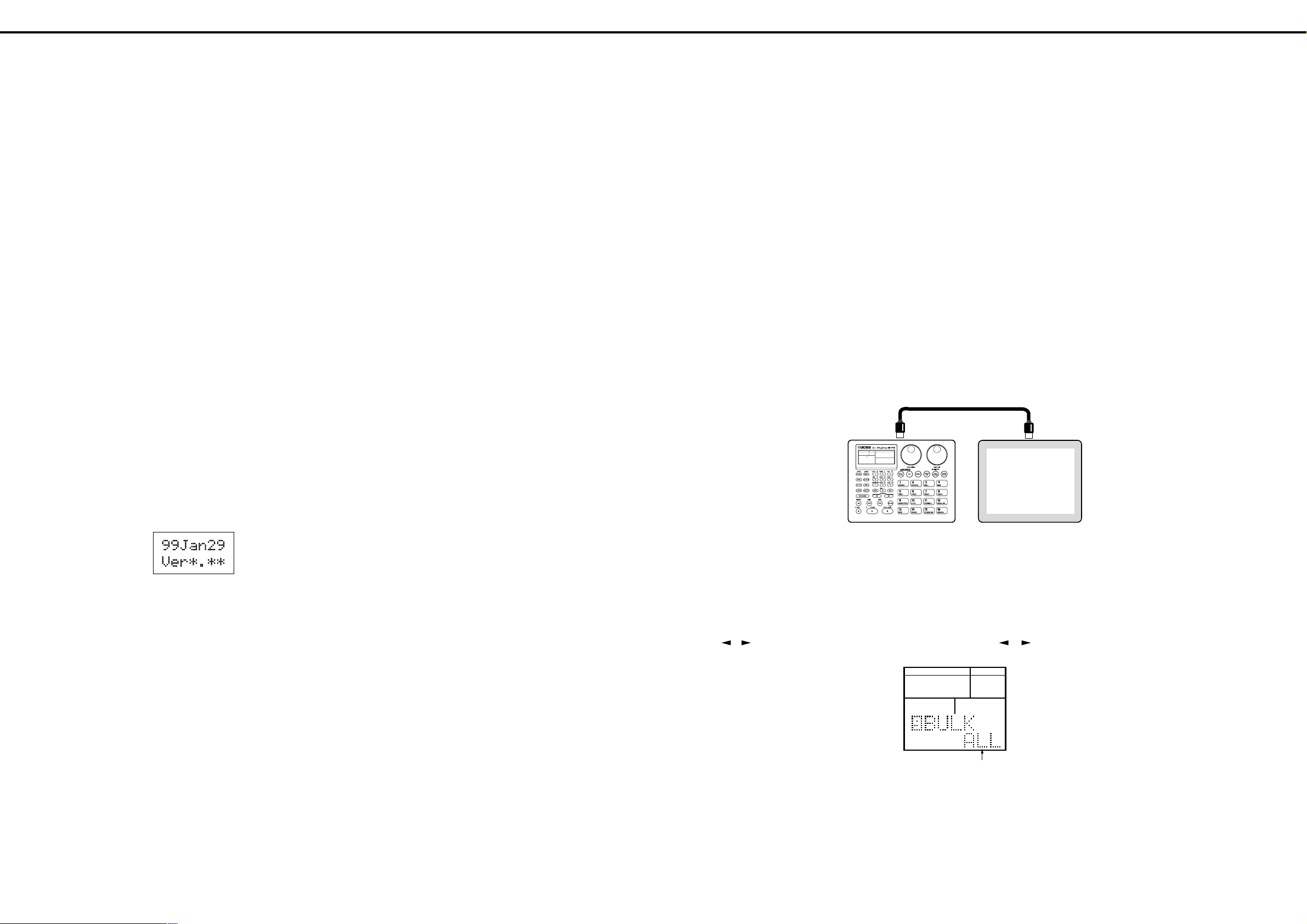
Connections
Procedure
1. Press [MIDI] to make “MIDI” light.
The DR-770 is now in MIDI mode.
2. Use [ ] [ ] to select “9 BULK.”
MIDI OUT
PAD BANKFUNCMODE
Transmit device (DR-770)
接続
MIDI IN
MIDI sequencer
Computer
etc.
MIDIシーケンサー
コンピューター
など
Receive device
受信側送信側(DR-770)
操作
1. [MIDI]を押してMIDIを点灯させます。
MIDIモードにします。
2. [ ][ ]を押して、9BULKを選びます。
6
Page 7

DR-770 Feb. 1999
3. Use [DEC] [INC] or [VALUE] to select the type of data that
will be transmitted.
ALL: All data of the DR-770
SEQ: All patterns and songs
GLOBAL: DPP/roll/metronome/MIDI settings
DRMKITS: All user drum kits
1DRMKIT: A specified individual drum kit (If this data is
transmitted to the DR-770, the drum kit that is
currently selected on the receiving device will
change to the drum kit settings that were
received.)
4. Press [ENTER].
The display will ask “Sure?,” allowing you to confirm whether
you really want to execute the bulk dump.
QUANTIZE
NEXT PTN
PART
■ If you selected “1DRMKIT,” use [DEC] [INC] or [VALUE] to
select the drum kit whose data you want to transmit.
5. To execute the bulk dump, press [ENTER].
The display will indicate “Trnsmit” (transmitting) ' “Done,”
and the bulk dump will be completed.
If you decide to cancel, press [STOP/EXIT].
The bulk dump will be canceled, and the display will indicate
“Aborted."
3. [DEC][INC]または[VALUE]で、転送するデータを選び
ます。
ALL: DR-770のすべてのデータ
SEQ: パターンとソング全部
GLOBAL: DPP/ロール/メトロノーム/MIDIの設定
DRMKITS:ユーザー・ドラム・キット全部
1DRMKIT: ドラム・キットいずれか1つ(DR-770に転送
したときは、受信側で今選ばれているドラ
ム・キットが転送したドラム・キットの設定
になります。)
4. [ENTER]を押します。
Sure?とバルク・ダンプを実行しても良いかどうかを
確認するメッセージが表示されます。
BEAT
LENGTH
PATTERN
■ 1DRMKITを選んだときは、[DEC][INC] または
[VALUE] でデータを転送するドラム・キットを選びま
す。
バルク・ダンプを実行するときは、[ENT E R] を押しま
す。
5. Trnsmit(転送中)→Doneと表示されてバルク・
ダンプが完了します。
中止するときは[STOP/EXIT]を押します。
Abortedと表示されてバルク・ダンプを中止します。
How to load the User Data
Connections
MIDI OUT
MIDI sequencer
Computer
etc.
MIDIシーケンサー
コンピューター
など
Transmit device
Connections
1. Press [MIDI] to make “MIDI” light.
The DR-770 is now in MIDI mode.
2. Use [ ] [ ] to select “2 MIDIch.”
3. Use [VALUE*] to select the MIDI channel.
■ If you want to restore data that was formetly transmitted to a
sequencer, set the unit to the same MIDI channel that was used
when transmitting the data.
■ If you want to receive data that being transmittied from another
DR-770, set both DR-770 units to the same MIDI channel.
4. Use [
] [ ] to select “7 RxEXC.”
SONG
PATTERN
PAD
UTILITY
QUANTIZE
NEXT PTN
PART
ユーザーデータのロード方法
接続
MIDI IN
PAD BANKFUNCMODE
Receive device (DR-770)
受信側(DR-770)送信側
操作
1. [MIDI]を押してMIDIを点灯させます。
MIDIモードにします。
2. [ ][ ]を押して、2MIDIchを選びます。
3. [VALUE*]で、MIDIチャンネルを設定します。
■ シーケンサーに転送したデータを戻すときは、データを
転送したときと同じMIDIチャンネルに設定します。
■ 別のDR-770から送信されるデータを受信するときは、2台
のDR-770を同じMIDIチャンネルに設定します。
][ ]を押して、7RxEXCを選びます。
4. [
FUNCMODE
INSERT
REAL
COPY
STEP
MIDI
DELETE
BEAT
LENGTH
PATTERN
EFFECTS
5. Use [DEC] [INC] or [VALUE] to turn the setting “ON.”
With playback stopped on the DR-770, receive the data.
5. [DEC][INC]または[VALUE]で、ONにします。
DR-770の演奏がストップしている状態で、データを受信
します。
7
Page 8

DR-770 Feb. 1999
Turning the encoder
(or<<<<<<<)
回す
TEST MODE
CAUTION : When running a test item (RAM check) in the test
mode the backup data in the mainframe will be erased.
Be sure to seve the data before running this test.
To save the data refer to “DATA SAVE AND LOAD”.
Required Items
· Monitor speakers or Headphones,
· MIDI cable
· FS5U× 2 (Polarity switch setting is Jack side)
· Oscilloscope
To enter test mode
While simultaneously pressing the [SONG] and [7] buttons, turn
the power on. The version number will appear on the LCD
display as shown below. The displayed date differs depending on
the ROM version.
テストモード
注意:テスト・モード内のテスト項目RAMチェックを
実行すると、本体内にバックアップしているユーザー・
データが消去されてしまいますので、必ず、データのセー
ブを行って下さい。データのセーブ方法は、データの
ロード/セーブの方法を参照して下さい。
用意するもの
・ モニター・スピーカーかヘッドホン、・MIDIケーブル
・フットスイッチ FS5U×2、(尚、ポラリティSW を
ジャック側に設定してください)
・ オシロスコープ
テストモードへの入り方
[SONG]ボタンと数字ボタン[7]を同時に押しながら電源を
入れます。
LCDディスプレイに下記のように表示されます。
日付はROMのバージョンによって違います。
NOTE : Each test number corresponds to the [0] to [7] keys on
numeric buttons. To begin a test, press a numeric button that
corresponds to the test number to be run.
[0]. LED check
This test checks whether the LED lights normally.
1. Press the numeric button [0] to run this test.
2. If normal, pressing the [REC] button turns on the red LED,
while pressing the [START] button turns on the green LED.
3. When pressing the [STOP/EXIT] button, the display will
show “OK”.
4. Again, press the [STOP/EXIT] button to return to the main
screen.
[1]. Switch check
This test checks whether each key (except key-pads) and the
encoder (VALUE knob) are functioning.
1. Press the numeric button [1] to run this test.
The display will show as follows:
注意:各テスト項目は、数字ボタンの[0]から[7]に対応
しています。
実行したいテスト項目に対応している数字ボタンを押し
て、テストを実行して下さい。
[0].LEDチェック
LEDのチェックを行います。
1. 数字ボタン[0]を押し、テストを実行させます。
2. [REC]ボタンを押すと赤のLEDが、[START]ボタンを
押すと緑のLEDが点灯します。
3. [STOP/EXIT]ボタンを押すと、LCDディスプレイに、
OKと表示されます。
4. もう一度[STOP/EXIT]ボタンを押すと、メイン画面に
戻ります。
[1].スイッチ・チェック
各ボタン(キー・パッド以外)とエンコーダー([VALUE]
ツマミ)のチェックを行います。
1. 数字ボタン[1]を押し、テストを実行させます。
LCDディスプレイに、下記のように表示されます。
This LCD display is referred to as the main screen in the
following procedures.
To exit test mode
On the main screen, press the [8] button.
The display will show “INIT?”.
When initializing:
Press the [ENTER] button. The display will show “Sure?”.
Press the [ENTER] button again. The display will show “Done”
and the operation will exit test mode.
When not initializing:
Press the [STOP/EXIT] button. The display will show “Aborted”
and the operation will exit test mode without initializing the
setting.
Test Items
The test mode includes the 8 tests.
0. LED check
1. Switch check
2. LCD check
3. RAM check
4. ROM check
5. MIDI check
6. FSR (Key Pads) check
7. OUTPUT check
以下の文章において、この画面を、メイン画面と呼びま
す。
テストモードの抜け方
メイン画面の状態で、数字ボタン[8]を押します。
すると、LCDディスプレイに、INIT?と表示されます。
・イニシャライズして終了する場合:
[ENTER]ボタンを押すと、LCDディスプレイに、Sure?
と表示されます。
もう一度[ENTER]ボタンを押すと、Doneと表示され、
テスト・モードから抜けます。
・イニシャライズせず終了する場合:
[STOP/EXIT]ボタンを押すと、LCD ディスプレイに、
Abortedと表示され、テスト・モードから抜けられま
す。
テスト項目
テストは全部で8項目あります。
0. LEDチェック
1. スイッチ・チェック
2. LCDチェック
3. RAMチェック
4. ROMチェック
5. MIDIチェック
6. FSR(キー・パッド)チェック
7. OUTPUTチェック
2. When pressing a button or Foot SW to be checked, the key
name will be displayed in the “
the same time a rim-shot sound will be output from Outputs L
and R.
3. After all the buttons and Foot SW have been pressed for
checking, the test automatically enters the encoder checking.
The display will show as follows:
4. When turning the encoder clockwise (or counterclockwise),
the display shown at right in the figure above will appear.
Then when turning the encoder in the reverse direction, the
display will show “OK” if the encoder is functioning.
5. Press the [STOP/EXIT] button to return to the main screen.
” field. At
[2]. LCD check
1. Press the numeric button [2] to run this test.
2. When this test is entered, all segments of the LCD will be
displayed.
3. When pressing the [STOP/EXIT] button, the display will
show “OK” (even if the LCD does not operate normally).
4. Again, press the [STOP/EXIT] button to return to the main
screen.
2. 任意のボタン(キー・パッド以外)を押すと、■■■
■■■■の部分に押したボタンの名前が表示され、同
時に、リムショットの音が、OUTPUTL/Rジャックか
ら出力されます。
3. 全てのボタン(キー・パッド以外とフットスイッチ)を
押すと、自動的にエンコーダーのチェックに入ります。
LCDディスプレイに、下記のように表示されます。
4. エンコーダーを右または左に回すと、上図、右のように
表示されます。
次に反対側に回すと、LCDディスプレイに、OKと
表示されます。
5. [STOP/EXIT]ボタンを押すと、メイン画面に戻りま
す。
[2].LCDチェック
1. 数字ボタン[2]を押して、テストを実行させます。
2. LCDを全て表示させます。
3. [STOP/EXIT]ボタンを押すと、LCDディスプレイに、
OKと表示されます。(LCDの表示がおかしい場合
でも)
4. もう一度、[STOP/EXIT]ボタンを押すと、メイン画面
に戻ります。
8
Page 9

DR-770 Feb. 1999
Pad no. / 1
L
TOM1
2
R
TOM2
3
IND1
TOM3
Output destination /
Sound /
パッド番号
出力ジャック
出力音
[3]. RAM check
1. Press the numeric button [3] to run this test.
This test automatically performs the RAM check.
If normal, the display will show “OK”. If a malfunction is
found, the display will show “NG”.
2. Press the [STOP/EXIT] button to return to the main screen.
[4]. ROM check
1. Press the numeric button [4] to run this test.
This test automatically performs the ROM check.
If normal, the display will show “OK”. If an error occurs, the
display will show as follows.
· If there is an error on the wave ROM
· If there is an error on the program ROM
· If there is an error on the wave ROM and program ROM
[3].RAMチェック
1. 数字ボタン[3]を押して、テストを実行させます。
自動的にRAM のチェックを行います。正常ならば、
LCDディスプレイに、OKと表示され、異常があれ
ばNGと表示されます。
2. [STOP/EXIT]ボタンを押すと、メイン画面に戻りま
す。
[4].ROMチェック
1. 数字ボタン[4]を押して、テストを実行させます。
自動的にROM のチェックを行います。正常ならば、
LCDディスプレイに、OKと表示され、異常があれ
ば以下のように表示されます。
・ WAVEROMがNG
・ プログラムROMがNG
・ WAVEROMとプログラムROMの両方がNG
2. In the “ ” field the key-pad number is displayed, and in
the “
An asterisk “*” is displayed when the pressure value reaches
“127”.
When a key-pad is pressed, the red LED first goes on and
then the green LED turns on when the pressure reaches
“127”.
A beep of oscillation sound is output from the OUTPUT-L/R
jacks.
If the FSR pattern touches a key-pad or two key-pads are
pressed simultaneously, the display will show “T” to the right
of the key-pad number as shown in the figure below.
At the same time, the key-pad number being touched will be
displayed at the lower right of the LCD display.
3. When all the key-pads are pressed with a pressure of more
than 127 and there is no pattern touch in the FSR, the display
will show “OK”. If the pressure value is low or any pattern
touch occurs, the display will show “NG”.
4. Press the [STOP/EXIT] button to return to the main screen.
” field the pressure value is indicated.
2. □□に、押したキー・パッドの番号、■■■に
は押したときの圧力値が表示されます。*は、圧力
値が127になると表示されます。
また、キー・パッドを押すと、最初に赤のLEDが点灯
し、圧力値が127になると緑のLEDが点灯します。
OUTPUT-L/Rジャックから、ピーという発振音が
出力されます。この時、FSR(キー・パッド)のパター
ンがタッチしていた場合、または、2つのキー・パッド
を同時に押した場合は、下記のように、Tがキー・
パッド番号の右側に表示されます。同時に、タッチして
いるキー・パッドの番号が、LCDディスプレイ右下に
表示されます。
3. 全てのキー・パッドが、それぞれ127以上の圧力
値で押され、FSR(キー・パッド)にパターン・タッチ
がなければ、LCDディスプレイに、OKと表示され
ます。
押したときの圧力値が低かったり、パターン・タッチ
あったときは、NGと表示されます。
4. [STOP/EXIT]ボタンを押すと、メイン画面に戻りま
す。
2. Press the [STOP/EXIT] button to return to the main screen.
[5]. MIDI check
1. Before entering this test, connect MIDI IN to OUT using the
MIDI cable.
2. Press the numeric button [5] to run this test.
If the test result is normal the display will show “OK”.
If the test is entered before connecting the MIDI cable, the
display will show “NG”. Connect the MIDI cable properly
and the display will change to “OK”.
3. Press the [STOP/EXIT] button to return to the main screen.
[6]. FSR (key-pads) check
This test checks whether the FSR (key-pads) is functioning.
1. Press the numeric button [6] to run this test.
The display will show as follows:
2. [STOP/EXIT]ボタンを押すと、メイン画面に戻りま
す。
[5].MIDIチェック
1. テストを実行する前に、MIDIケーブルで、MIDIIN と
OUTを接続します。
2. 数字ボタン[5]を押して、テストを実行させます。
自動的にチェックを行い、正常ならば、LCDディスプ
レイに、OKと表示され、異常があればNGと表
示されます。
(MIDIケーブルで、MIDIINとOUTを接続しないで、
テストを実行した場合、NGと表示されますが、
MIDIケーブルで接続すると、OKと表示されま
す。)
3. [STOP/EXIT]ボタンを押すと、メイン画面に戻りま
す。
[6].FSR(キー・パッド)チェック
FSR(キー・パッド)のチェックを行います。
1. 数字ボタン[6]を押して、テストを実行させます。
LCDディスプレイに、下記のように表示されます。
[7]. Sound check
This performs the tests for sounding and panning.
1. Press the numeric button [7] to run this test.
The display will show as follows:
K Sounding
2. In the “ ” field the output destination is displayed, and
in the “
3. When you press one of key-pads 1 to 4, sound will be output
as shown in the table below.
” field the velocitiy is indicated.
[7].サウンド・チェック
音出しとパンニングのテストを行います。
1. 数字ボタン[7]を押して、テストを実行させます。
LCDディスプレイに、下記のように表示されます。
○ 音出し
2. □□は出力ジャック名、■■■には押された時
の圧力値が表示されます。
3. キー・パッドの1〜3を押すと、それぞれ下表
のように音が出力されます。
9
Page 10

DR-770 Feb. 1999
K EQ (IC106 on Jack Board)
4. When you press one of key-pads “5” to “7”, a rectangle wave
will be output with following EQ setting.
Pad no. / 5
EQ High
EQ Low
LCD display /
<Fig 1> L(MONO)
R
パッド番号
LCD表示
Pad No. 5 Pad No. 6 Pad No. 7
K Panning
5. When you press one of key-pads 13 to 15, a sine wave will be
output with the follwing panning.
Pad no. / 13
パッド番号
パンニング
○ EQ(IC106orJackBoard)
4. キー・パッドの5〜7を押すと、それぞれ下表
のようなEQ設定で矩形波が出力されます。
7
+12dB
-12dB
-12 +12
(1v/div)
(2ms/div)
0dB
0dB
00
6
-12dB
+12dB
+12 -12
○ パンニング
5. キー・パッドの13〜15を押すと、下表のよう
なパンニングで正弦波が出力されます。
L7
14
CENTER
15
R7Panning /
<Fig 2> L(MONO)
R
Pad No. 13 Pad No. 14 Pad No. 15
6. The LCD is displayed as shown below.
7. In the “ ” field the panning state is displayed, and in the
“
” field the pressure value is indicated.
An asterisk “*” is displayed when the pressure value reaches
“127”.
When a key-pad is pressed, the red LED first goes on and
then the green LED turns on when the pressure reaches
“127”.
8. When pressing the [STOP/EXIT] button, the display will
show “OK”.
9. Again, press the [STOP/EXIT] button to return to the main
screen.
(1v/div)
(2ms/div)
6. LCDディスプレイには、下記のように表示されます。
7. □□にパンニング状態、■■■には押された時
の圧力値が表示されます。*は、圧力値が127
になると表示されます。
また、キー・パッドを押すと、最初に赤のLEDが点灯
し、圧力値が127になると緑のLEDが点灯します。
8. [STOP/EXIT]ボタンを押すと、LCDディスプレイに、
OKと表示されます。
9. もう一度、[STOP/EXIT]ボタンを押すと、メイン画面
に戻ります。
10
Page 11

DR-770 Feb. 1999
TROUBLESHOOTING
q No sound is produced.
possible causes
The volume is set to minimum.
The level of the key-pads is set to zero.
The selected Rhythm Pattern or Song contains on data.
w Sound breaks.
possible causes
More than 14 voices are being played simultaneously.
Assign Type for the key-pads is not properly set.
e Sound is strange.
possible causes
The settings for the key-pads are inappropriate.
r The Roll/Flam effect is not produced.
possible causes
The Flam Interval is set to zero.
The settings for the Flam Ratio are inappropriate.
トラブルシューティング
q 音が出ない。
原因
ボリュームが最小になっている。
キーパッドのレベルが0になっている。
現在選ばれているソング、またはリズム・パターンに
データが記憶されていない。
パンの設定が、INDIVになっている。
w 音が途切れる。
原因
同時に14音以上の音色を鳴らしている。
キー・パッドのアサイン・タイプが不適当。
e 音色がおかしい。
原因
キー・パッドの設定が不適当。
r ロール/フラムができない。
原因
ロールの設定で、タイプがFLになっている。
フラム・インターバルやフラム・レシオの設定が不適
当。
!0 The metronome does not sound.
possible causes
The level of the metronome is set to zero.
!1 Program Change messages cannot be transmitted or
received.
possible causes
“4PRG’ in the MIDI Mode is set to OFF.
!2 The volume does not change when MIDI Volume messages
are received.
possible causes
“5RxVOL” in the MIDI mode is set to OFF.
!3 The volume does not change when MIDI Expression
messages are received.
possible causes
“6RxEXPR” in the MIDI mode is set to OFF.
!4 The DR-770 cannot receive Exclusive messages.
possible causes
“7RxEXC” in the MIDI mode is set to OFF.
MIDI channels are not set to the same number.
!0 メトロノームが鳴らない。
原因
メトロノームのレベルが0になっている。
!1 プログラム・チェンジが送受信されない。
原因
MIDIモードの4PRGがOFFになっている。
!2 MIDIボリューム情報で音量が変化しない。
原因
MIDIモードの5RxVOLがOFFになっている。
!3 MIDIエクスプレッション情報で音量が変化しない。
原因
MIDIモードの6RxEXPRがOFFになっている。
!4 エクスクルーシブ・メッセージを受信しない。
原因
MIDIのモードの7RxEXCがOFFになっている。
MIDIチャンネルが合っていない。
t Playback does not begin when [START] button is pressed.
possible causes
The Sync Mode is set to MIDI.
The selected Rhythm Pattern or Song contains no data.
y Songs automatically play one after another.
possible causes
The song chain function is ON.
u The tempo changes when a song starts playing.
possible causes
An internal tempo is being set.
i The DR-770 cannot be controlled by an external MIDI
device.
An external MIDI device cannot be controlled by the DR-
770.
possible causes
The MIDI channels of the DR-770 and the external MIDI
device do not match.
Note numbers of the DR-770 and the external MIDI device do
not correspond.
t [START]ボタンを押しても演奏がスタートしない。
原因
シンク・モードがMIDIになっている。
現在選ばれているソングまたはリズム・パターンにデー
タが記憶されていない。
y ソングの演奏が終了したら、他のソングが自動的にス
タートする。
原因
ソング・チェインが設定されている。
u ソングの演奏をスタートすると、テンポが変化する。
原因
イニシャル・テンポが設定されている。
i 外部MIDI機器から音が鳴らせない。
外部MIDI機器の音が鳴らない。
原因
MIDIチャンネルが合っていない。
ノート・ナンバーが合っていない。
o When the DR-770 is played by performance data from a
sequencer, the song on the DR-770 starts together.
possible causes
The Sync Mode is set to MIDI sync.
o シーケンサーの演奏データでDR-770を鳴らす時に、DR-
770のソングが一緒にスタートする。
原因
シンク・モードがMIDIになっている。
11
Page 12

DR-770 Feb. 1999
ERROR MESSAGE
If you attempt an incorrect operation or if an operation could not be
executed, the display will indicate an error message. Refer to this
list and take the appropriate action.
● No more patterns can be recorded.
❍ Press [STOP/EXIT]. If you want to continue recording patterns,
you must first delete unneeded patterns. (p. 62)
● No more songs can be recorded.
❍ Press [STOP/EXIT]. If you want to continue recording songs,
you must first delete unneeded songs. (p. 67)
/エラー・メッセージ
操作を誤ったり、正しく実行できなかったときは、ディスプ
レイにエラー・メッセージが表示されます。表示のメッセー
ジにしたがって対処してください。
● パターンをこれ以上記憶することはできません。
❍ [STOP/EXIT]を押してください。パターンの録音を続
ける場合は、不要なパターンを削除してください。
(P.62)
● ソングをこれ以上記憶することはできません。
❍ [STOP/EXIT]を押してください。ソングの録音を続け
る場合は、不要なソングを削除してください。(P.67)
● During song editing, using “Copy Song” or “Delete Song,” the
selected song contained no data.
❍ Press [STOP/EXIT], then select a different song.
● An excessive amount of MIDI data was received all at once, and
the DR-770 was unable to process it.
Press [STOP/EXIT],
❍ If this message appears while receiving data, reduce the amount
of MIDI data that is being transmitted to the DR-770.
❍ Change the MIDI mode setting so unnecessary MIDI messages
are not transmitted or received. (p. 87)
● An exclusive message could not be received correctly.
❍ Press [STOP/EXIT], then try the operation once again.
● ソング編集の「ソングのコピー」や「ソングの削除」
で、対象となるソングにデータがありません。
❍ [STOP/EXIT]を押してから、ソングを替えてくださ
い。
● 大量のMIDI情報を受信したため、DR-770本体で処理しき
れなくなりました。
[STOP/EXIT]を押してから、
❍ 受信時に表示されたときは、送信側のMIDI情報を減らし
てください。
❍ 不必要なMIDI情報を送受信しないように、MIDIモードの
設定を行ってください。(P.87)
● エクスクルーシブ・メッセージが正しく受信できません
でした。
❍ [STOP/EXIT]を押してから、もう一度操作をやり直し
てください。
● During pattern editing, using “Copy Pattern” or “Delete
Pattern,” the selected pattern contained no data.
❍ Press [STOP/EXIT], then select a different pattern.
● During song editing, using “Insert Pattern” or “Delete Pattern,”
the selected pattern contained no data.
❍ Press [STOP/EXIT], then select a different part.
● パターン編集の「パターンのコピー」や「パターンの削
除」で、対象となるパターンにデータがありません。
❍ [STOP/EXIT]を押してから、パターンを替えてくださ
い。
● ソング編集の「パターンの挿入」や「パターンの削除」
で、対象となるパターンにデータがありません。
❍ [STOP/EXIT]を押してから、パートを替えてくださ
い。
● The memory backup battery inside the DR-770 has run down.
(This message will appear when the power is turned on.)
❍ Replace the battery as soon as possible. For battery
replacement, please contact a Roland Service Center.
● The data in internal memory has been lost. (This message will
appear when the power is turned on.)
❍ After this message is shown, “Press ENTER” appears, then
pressing [ENTER] will recall the factory settings.
● 本体のメモリー・バックアップ用の電池が消耗していま
す。(このメッセージは、電源投入時に表示されま
す。)
❍ 早めに電池を交換してください。交換に関しては、ロー
ランド・サービスにご相談ください。
● 本体に記憶されているデータが壊れています。(この
メッセージは、電源投入時に表示されます。)
❍ このメッセージが表示された後PressENTERと表示さ
れ、[ENTER]を押すと、製品出荷時の設定に戻ります。
12
Page 13

DR-770 Feb. 1999
A
BLOCK DIAGRAM
/ブロック図
B
C
D
E
F
G
H
I
J
K
L
M
N
O
P
Q
R
S
T
U
V
13
Page 14

DR-770 Feb. 1999
(
)
(
)
p
p
p
p
(3P)
p
p
(6P)
p
p
p
p
(5W)
(3W)
p
p
p
p
(
)
(
)
(up)
(right)
(
)
A
CIRCUIT DIAGRAM (JACK)
B
C
D
E
F
G
H
I
J
K
L
M
N
O
P
/回路図(JACK)
VR Board
To Jack Board
CN 101
ENC Board
To Jack Board
CN 103
Jack Board
To Main Board
CN1
To Main Board
CN2
CN301
6
6
5
5
4
4
3
3
2
2
1
1
WIRING HARNESS C
EN201A
EC16B24204
CN201
3
3
2
2
1
1
WIRING HARNESS B
CN104
1
1
2
2
3
3
4
4
5
5
6
6
WIRING 6P
CN102
1
1
2
2
3
3
4
4
5
5
6
6
7
7
8
8
9
9
10
10
11
11
WIRING 11P
IC101C
UPC4570
VR301A
RK14K124 50kB *2
235
146
VR301B
RK14K124 50kB *2
20
EN
AB
312
L101
SBT-0460
L102
SBT-0460
A
+
5D
D
A +8
84
+
A
10
VR301C
RK14K124 50kB *2
10
20
EN
AB
EN201B
EC16B24204
CN103
53254-0310
3
3
2
To ENC Board
2
1
CN201
1
R144 100
R145 120
R146 220
R147 220
IC102C
UPC4570
C130
0.1
ENTER
1 2
JK108
M-S2-3P
L108
SBT-0460
L109
SBT-0460
L110
SBT-0460
L111 SBT-0460
C160
0.1
D A
A +8
84
+
A
SW6
+
+
5D
5D
R102
D104
10k
1SS133
1 2
R103
1k
C102
100
D
R105
1k
C104
R106
18k
C106
100
2
3
2
3
C118
150
6
5
C126
150
~
+-
4 3
~
2 1
SW4
1 2
+
+
+
9
1
IC101A
UPC4570
A
IC103A
M5216FP
1
IC103B
M5216FP
7
SPUN19430A
100
SW101A
C108
10/16
CN101
6
6
5
5
4
4
3
3
2
2
1
1
53254-0610
C115
10/16
C123
10/16
C128
47/16
C133
47/16
L117
124
3.62, 5
SBT-0160W
1 2
DA4
1SS300
R111
1k
To VR Board
CN301
R117
1k
R125
1k
R128
3.3k
R134
3.3k
3
1 2
C136
470/25
R113
18k
R121
18k
1 2
R107
10k
C113
2.2/25
C121
2.2/25
VREF 4.0V
R138
JUMPER
0
C137
470/25
SW3
63
VREF 4.0V
VREF 4.0V
VREF 4.0V
D102
1G4B42
VREF 4.0V
C107
R101
56k
C101
10/16
C114
10/16
R119
56k
R120
56k
C122
10/16
1
3
425
524
A +8
IC103C
84
M5216FP
-
C131
0.1
+
R115
3.3k
VREF 4.0V
R123
3.3k
MIDI INMIDI OUT
1
3
425
524
C157
100
C158
0.1
D
C132
0.1
A
0.033
R109
3.3k
JK107
M-S2-3P
D
6
R110
7
3.3k
5
+
IC101B
UPC4570
C110
150
C112
0.033
2
R116
-
3.3k
3
+
C117
150
A
C120
0.033
6
R124
-
3.3k
5
+
C125
150
A AAA
C159
100
2 1
Q104
2SA1049
IC104
+
7805AHF
5D
3
OUT
C138
C139
100/6.3
0.1
A
D
A +9
VREF 4.5V
C154
470/16
A
1 2
DA2
1SS300
3
IC102A
UPC4570
1
IC102B
UPC4570
7
R129
10k
C134
47/16
COM
2
R142
4.7k
R143
4.7k
Q105
2SC2459
A
1
IN
C140
0.1
C142
100/16
SW1
^
1 2
C146
IC106
2.2/25
2
CH1IN
19
CH2IN
C147
3
2.2/25
SIMIN1
C148
0.022
4
SIMOUT1
C150
0.47
5
BASS1
9
DAT
10
CLK
11
CS
+
5D
12
DVDD
C152
0.1
8
DGND
D
M62421SP
R130
47k
3
1 2
3
1 2
Q106
2SC2459
C163
10/35
IC105
UPC24M09AHF
3
OUT
C143
0.1
7
OUT1
14
OUT2
18
SIMIN2
C149
0.022
17
SIMOUT2
C151
0.47
16
BASS2
C155 0.033
6
TRE1
15
TRE2
C156 0.033
1
REF
A +8
20
AVDD
C153
0.1
13
AGND
A
R131
10k
R135
R133
10k
560
12
D101
MTZ8.2B
R137
R136
5.6
COM
2
R139
15
1k
D103
MTZ5.6C
1 2
1
IN
C144
0.1
1 2
SW2
1 2
DA3
1SS300
D105
1SS133
1 2
D
+5D+
D106
1SS133
1 2
D107
1SS133
1 2
D
R112
56k
A A
R118
56k
A
A
R126
56k
R127
22
1/2W
A
R132
1/2W
22
A A
JK106
2
1
3
HEC0740-010-10
A
SW5
CHORUS
C111
0.0033
C119
0.0033
C127
0.0033
C103
100
D
5D
R104
10k
C105
100
DD
1
1
1
C129
0.0033
A
C135
0.0033
AC14V
2 3
2 3
2 3
L106
SBT-0460
L107
SBT-0460
L103
SBT-0460
Q101
DTC343TK
A
L104
SBT-0460
Q102
DTC343TK
A
L105
SBT-0460
Q103
DTC343TK
A
JK101
3
4
1
HLJ7001-01-3010
D
JK102
3
4
1
HLJ7101-01-3010
A
JK103
2, 3
4
1
HLJ7101-01-3010
A
JK104
2, 3
4
1
HLJ7101-01-3010
A
JK105
2
3
1
C161
YKB21-5130
100
A
C162
100
A
P12
P11
P10
P9
P8
P7
P6
P5
To Main Board(1/2)
P4
P3
P2
P1
P0
FOOT SWITCH
IND1
L/MONO
R
PHONES
1 2
DA7
1SS300
1 2
DA1 1
1SS300
1 2
DA1 5
1SS300
SW12
REVERB
1 2
SW20
DRUM KIT
1 2
SW28
TEMPOSTEP/REAL
1 2
Q
R
S
SW13
STOP/EXIT
1 2
SW21
START
1 2
SW7
FWD
1 2
SW14
BWD
1 2
SW22
RESET
1 2
1 2
DA8
1SS300
1 2
DA12
1SS300
SW15
>
1 2
SW23
<
left
1 2
1 2
DA5
1SS300
1 2
DA9
1SS300
1 2
DA13
1SS300
SW8
0
1 2
SW16
down
V
1 2
SW24
DELETE
1 2
SW9
2
1 2
SW17
1
1 2
SW25
MIDI
1 2
1 2
DA6
1SS300
1 2
DA1 0
1SS300
1 2
DA1 4
1SS300
SW10
5
1 2
SW18
4
1 2
SW26
EFFECT
1 2
SW11
8
1 2
SW19
7
1 2
SW27
1 2
T
1 2
DA18
1SS300
SW34
1 2
SW35
1 2
1 2
DA1 9
1SS300
SW36
ROLLPTN/SONGPAD
1 2
Main Board(2/2)
U
SW29
1 2
SW30
1 2
1 2
DA16
1SS300
SW31
PAD BANKFLAMREC
1 2
1 2
DA1 7
1SS300
SW32
1 2
SW33
UTILITYCOPY
1 2
V
14
Page 15

DR-770 Feb. 1999
A
CIRCUIT BOARD (JACK)
/基板図(JACK)
B
C
D
E
F
G
H
I
J
K
L
M
N
O
P
Q
View from component side.
R
S
T
U
V
15
Page 16

DR-770 Feb. 1999
A
CIRCUIT DIAGRAM (MAIN)
RA1
P12
B
C
D
E
F
G
H
I
J
K
L
M
N
O
P
Q
R
S
T
U
To Main Board(2/2)
MIDI OUT 2
MIDI IN 1
MIDI IN 2
LED1
R6
SLC-22VR
330
D
LED2
R8
SLC-22MG
270
D
+
BAT
5D
DA1
RB715F
1 2
3
F16
F15
F14
F13
F12
F11
F10
F9
F8
F7
F6
F5
F4
F3
F2
F1
A
CN3
17
17
16
F16 F16
16
15
F15
15
14
F14
14
13
F13
13
12
F12
12
11
F11
11
10
F10
10
9
F9
9
8
F8
8
7
F7
7
6
F6
6
5
F5
5
4
F4
4
3
F3
3
2
F2
2
1
F1
1
To FSR
(Key-Pads)
MIDI OUT 1
2SA1037KR
12
12
(CR2032)
4
2
5
1
11
15
14
12
9
10
6
D
4
2
5
1
11
15
14
12
9
10
6
D
Q3
+
BT1
IC11
3Y
2Y
1Y
0Y
3X
2X
1X
0X
B
A
INH
IC13
TC 7 4HC4052
3Y
2Y
1Y
0Y
3X
2X
1X
0X
B
A
INH
5D
DA20
1SS300
1 2
3
Q1
+
5D
DTA114TK
2
3 1
Q2
+
5D
DTA114TK
2
3 1
R12
10k
1 2
C13
47/16
4HC4052
YCOM
XCOM
YCOM
XCOM
RA5
CNB2B9Z3.3K
1 2
3
4
5
6
7
8
9
1 2
3
4
5
6
7
8
9
RA6
CNB2B9Z3.3K
+
5D
1
3
P12
P11
P10
P9
P8
P7
P6
P5
P4
P3
P2
P1
P0
TC 7 4AC14AF
D
VCC
GND
VEE
VCC
GND
VEE
R36
33k
2
IC2A
12
R11
33k
R13
100k
D
3
13
16
8
7
3
13
16
8
7
F11
F10
F9
F12
F14
F16
F15
F13
F3
F2
F1
F4
F6
F8
F7 F2
F5
+
5D
P11
P10
P9
P8
P7
P6
P5
P4
P3
P2
P1
P0
IC7
PC410
1
3
FS1
FS0
+
+
R41
10k
+
5D
7
4
A
D
IC2F
TC 7 4AC14AF
64
+
5D
R9
47k
6
5
R14
2.2M
D
5D
C14
0.1
5D
C20
0.1
A
F[16..1]
C31
220p
C33
220p
C37
220p
C40
220p
C43
220p
C46
220p
C49
220p
C52
220p
A
R37
4.7k
VCC
GND
RCE9A103
1 2
D
1312
+
5D
5
IC1B
BA10393F
C32
220p
C34
220p
C38
220p
C41
220p
C44
220p
C47
220p
C50
220p
C53
220p
+
5D
IC20
6
M51954BFP
NC
RST
NC
NC
NC
DLY
3
4
5
6
7
8
9
C8
0.1
D
7
F15
F14
F13
F12
F11
F10
F9
F8
F7
F6
F5
F4
F3
F1
IC2D
TC 7 4AC14AF
9 8
1
2
3
8
5
+
5D
R40
1k
+
5D
R10
22k
C61
1/50
P8
P7
P6
P5
P12
P11
P10
P9
R39
10k
D
/回路図(MAIN)
Main Board(1/2)
+
P[12..0]
+
5D
IC6
HD6415108F
R1
10k
111
MD2
110
MD1
109
+
P0
P1
P2
P3
P4
P5
P6
P7
P8
P9
P10
P11
P12
5D
D
C18
100/6.3
A
R28
1M
C56
22P
MD0
112
STBY
96
TXD2/P87
95
RXD2/P86
92
SCK2/IRQ3/P83
94
TXD1/P85
93
RXD1/P84
91
SCK1/IRQ2/P82
80
P67
79
P66
78
P65
77
P64
76
P63
75
P62
74
P61
73
P60
72
P57
71
P56
70
P55
69
P54
68
P53/FTOB2
67
P52/FTOA2
66
P51/FTOB1
65
P50/FTOA1
63
P47/FTCI2
62
P46/FTI2
61
P45/FTCI1
60
P44/FTI1
59
P43/TMO
58
P42/TMRI
57
P41/TMCI
56
P40/ADTRG
54
P37
53
P36
52
P35
51
P34
50
P33
86
AN3/P73
85
AN2/P72
84
AN1/P71
83
AN0/P70
87
AVCC
82
AVSS
98
EXTAL
99
XTAL
1
RES
IC3C
TC 7WU04F
6 2
X1
MA-406 24MHz
1 4
D
+
5D
C17
0.1
108
VCC55VCC88VCC
VSS3VSS20VSS37VSS46VSS64VSS81VSS97VSS
IC3B
TC 7WU04F
3 5
R33
220
C57
22P
D
+
5D
IC1A
BA10393F
3
1
2
5D
C7
0.1
D
45
P27/A23
44
D
P26/A22
P25/A21
P24/A20
P23/A19
P22/A18
P21/A17
P20/A16
P30/WAIT
P32/BREQ
P31/BACK
P81/IRQ1
P80/IRQ0
100
R47
100
P17/D7
P16/D6
P15/D5
P14/D4
P13/D3
P12/D2
P11/D1
P10/D0
A15
A14
A13
A12
A11
A10
D15
D14
D13
D12
D11
D10
HWR
LWR
RFSH
NMI
PHAI
A21
43
A20
42
A19
41
A18
40
A17
39
A16
38
A15
36
A14
35
A13
34
A12
33
A11
32
A10
31
A9
30
A9
A8
29
A8
A7
28
A7
A6
27
A6
A5
26
A5
A4
25
A4
A3
24
A3
A2
23
A2
A1
22
A1
A0
21
A0
D7
19
D6
18
D5
17
D4
16
D3
15
D2
14
D1
13
D9
D0
12
D8
11
10
9
8
7
6
5
4
105
106
104
RD
103
AS
47
49
48
107
90
89
2
101
102
E
C66
27p
D
R15
220
R16
220
R17
220
D
R29
180
D
R44
100
R45
100
IC2C
TC 7 4AC14AF
56
IC2B
TC 7 4AC14AF
1110
IC2E
TC 7 4AC14AF
D[7..0]
IC9
D7
46
DB7
D6
45
DB6
D5
44
DB5
D4
43
DB4
D3
42
DB3
D2
41
DB2
D1
40
DB1
D0
39
DB0
36
RS
37
R/W
38
E
D
+
5D
R21
1k
R23
2.2k
R25
2.2k
R26
2.2k
R27
2.2k
D
D
24
+
R24
2.2k
C64
10p
C65
10p
OSC1
5D
R22
91k
25
OSC2
30
V5
29
V4
28
V3
27
V2
26
V1
+
5D
33
VDD
C39
0.1
23
VSS
SED1278F0A
D
IC1C
84
BA10393F
C1
0.1
DD
+
5D
R3
R4
100k
100k
+
D
D
62
61
60
59
58
57
56
55
54
53
52
51
50
49
48
47
63
64
65
66
67
68
69
70
71
72
73
74
75
76
77
78
79
80
1
2
3
4
5
6
7
8
9
10
11
12
13
14
15
16
17
18
19
20
21
22
31
32
34
35
R7
100k
RA2
RCE9A103
+
5D
1 2
41
42
43
44
45
46
47
48
49
50
51
52
53
54
55
56
1
2
3
4
5
6
7
8
9
10
11
12
13
14
15
16
17
18
19
20
21
22
23
24
25
26
27
28
29
30
31
32
33
34
35
36
37
38
39
40
5D
R5
100k
LCD1
COM16
COM15
COM14
COM13
COM12
COM11
COM10
COM9
COM8
COM7
COM6
COM5
COM4
COM3
COM2
COM1
SEG40
SEG39
SEG38
SEG37
SEG36
SEG35
SEG34
SEG33
SEG32
SEG31
SEG30
SEG29
SEG28
SEG27
SEG26
SEG25
SEG24
SEG23
SEG22
SEG21
SEG20
SEG19
SEG18
SEG17
SEG16
SEG15
SEG14
SEG13
SEG12
SEG11
SEG10
SEG9
SEG8
SEG7
SEG6
SEG5
SEG4
SEG3
SEG2
SEG1
RCD1627R
C10
0.01
34
C11
0.01
COM16
COM15
COM14
COM13
COM12
COM11
COM10
COM9
COM8
COM7
COM6
COM5
COM4
COM3
COM2
COM1
SEG40
SEG39
SEG38
SEG37
SEG36
SEG35
SEG34
SEG33
SEG32
SEG31
SEG30
SEG29
SEG28
SEG27
SEG26
SEG25
SEG24
SEG23
SEG22
SEG21
SEG20
SEG19
SEG18
SEG17
SEG16
SEG15
SEG14
SEG13
SEG12
SEG11
SEG10
SEG9
SEG8
SEG7
SEG6
SEG5
SEG4
SEG3
SEG2
SEG1
LP
XSCL
FR
DO
IC2G
TC 7 4AC14AF
ENCORDER A
ENCORDER B
9
8
7
6
5
4
3
+
5D
147
C67
0.1
D
D7
D6
D5
D4
D3
D2
D1
D0
A0
IC3D
TC 7WU04F
A18
A17
A16
A15
A14
A13
A12
A11
A10
A9
A8
A7
A6
A5
A4
A3
A2
A1
A0
A19
A[21..0]
A16
A15
A14
A13
A12
A11
A10
A9
A8
A7
A6
A5
A4
A3
A2
A1
A0
A20
BAT
2 4
A19
A18
A17
A20
A21
53
+
5D
84
C68
0.1
IC14
TC7S04F
D
IC3A
TC 7WU04F
C3
1 7
0.1
D
3
2
1
5
4
6
C
B
A
G2B
G2A
G1
31
30
2
3
29
28
4
25
23
26
27
5
6
7
8
9
10
11
12
22
24
IC8
LH53H4100
A18
A17
A16
A15
A14
A13
A12
A11
A10
A9
A8
A7
A6
A5
A4
A3
A2
A1
A0
CE
OE
D[7..0]
D
+
5D
16
Y7
Y6
VCC
Y5
Y4
Y3
Y2
Y1
Y0
GND
8
D
D
D7
D6
D5
D4
D3
D2
D1
D0
VPP
VCC
VSS
IC12
2
A16
31
A15
3
A14
28
A13
4
A12
25
A11
23
A10
26
A9
27
A8
5
A7
6
A6
7
A5
8
A4
9
A3
10
A2
11
A1
12
A0
30
CE2
22
CE1
29
R/W
24
OE
TC551001CF-70L
C25
0.1
7
9
10
11
12
13
14
15
IC17
TC7 4AC138F
IC5
TC6116AF
+
5D
114
XMSF
113
X68
112
XE
D
66
CA19
67
D7
21
D6
20
D5
19
D4
18
D3
17
D2
15
D1
14
D0
13
A5
A4
+
5D
A3
A2
1
32
16
D
A1
A0
21
20
19
18
17
15
14
13
BAT
1
32
16
+
5D
53
IC18
TC7S02F
D
D7
D6
D5
D4
D3
D2
D1
D0
D7
D6
D5
D4
D3
D2
D1
D0
C16
0.1
D
R49
10k
D
C26
0.1
D
4
C12
0.1
D
I/O8
I/O7
I/O6
I/O5
I/O4
I/O3
I/O2
I/O1
NC
VDD
VSS
1
2
69
D
68
70
71
+
5D
74
73
76
80
75
77
79
81
84
86
85
87
89
93
95
94
92
88
+
5D
99
100
78
72
97
102
107
115
111
110
109
108
101
116
98
82
83
118
117
52
96
53
56
57
65
64
63
62
61
60
59
58
103
105
46
47
48
49
50
51
ED7
ED6
ED5
ED4
ED3
ED2
ED1
ED0
IC19
MB622928PF-G-BND
CA18
CA17
CA16
CA15
CA14
CA13
CA12
CA11
CA10
CA5
CA4
CA3
CA2
CA1
CA0
CD7
CD6
CD5
CD4
CD3
CD2
CD1
CD0
RESET
ALE
DS(RD)
R/W(WR)
CS
WAIT
GPINT
EXWAIT
INT5
INT4
INT3
INT2
GAINT
CS7
CS6
CS5
CS4
CS3
CS2
CS1
CS0
RSCD
RWWR
LERD
LD7
LD6
LD5
LD4
LD3
LD2
LD1
LD0
IOCK
CK
SC5
SC4
SC3
SC2
SC1
SC0
1
5
23
22
21
20
19
4
3
2
17
16
7
EWE
CK
ED7
ED6
ED5
ED4
ED3
ED2
ED1
ED0
CR
CC
RESET
VDD18VDD54VDD90VDD
GND19GND55GND91GND
104
+
5D
12
VDD
VSS
6
+
5D
C2 0.1
C4 0.1
C5 0.1
C6 0.1
126
DACA(LE)
DACC(MX)
DACB(INH)
GND
GND
127
142
D
24
VDD
SCK
WDTH2
WDTH1
WDTH0
VSS
18
D
WA19
WA18
WA17
WA16
WA15
WA14
WA13
WA12
WA11
WA10
WA9
WA8
WA7
WA6
WA5
WA4
WA3
WA2
WA1
WA0
WD7
WD6
WD5
WD4
WD3
WD2
WD1
WD0
WCS7
WCS6
WCS5
WCS4
WCS3
WCS2
WCS1
WCS0
EA14
EA13
EA12
EA11
EA10
EA9
EA8
EA7
EA6
EA5
EA4
EA3
EA2
EA1
EA0
ED7
ED6
ED5
ED4
ED3
ED2
ED1
ED0
EWE
ECS
SD
SCK
TEST
C62
0.1
D
SD
LE
NC
9
11
10
8
15
14
13
134
135
137
136
138
139
141
140
4
7
2
144
143
1
3
5
6
8
9
11
10
12
14
16
20
17
15
13
133
132
131
130
129
128
125
124
45
42
43
36
33
38
40
41
39
37
35
34
32
30
28
29
27
25
23
21
22
24
26
44
31
119
121
120
122
123
106
WA[21..0]
D
WA19
WA18 WA11
WA17
WA16
WA15
WA14
WA13
WA12
WA11
WA10
WA9
WA8
WA7
WA6
WA5
WA4
WA3
WA2
WA1
WA0
WD6
WD5
WD4
WD3
WD2
WD1
WD0
WA20
WA21
ED7
ED6
ED5
ED4
ED3
ED2
ED1
ED0
R34 1k
R35 1k
R32 1k
D
WA0
WA21
WA20
WA19
WA18
WA17
WA16
WA15
WA14
WA13
WA12
WA10
WA9
WA8
WA7
WA6
WA5
WA4
WA3
WA2
WA1
WD[7..0]WD7
RA7
1 8
2 7
3 6
4 5
EXBV8V103
D
R18 1k
R19 1k
R20 1k
IC16
BU9480F
5
LRCK
7
BCLK
6
SDAT
44
A20
43
A19
2
A18
3
A17
34
A16
35
A15
36
A14
37
A13
38
A12
39
A11
40
A10
41
A9
42
A8
4
A7
5
A6
6
A5
7
A4
8
A3
9
A2
10
A1
11
A0
12
CE
14
OE
33
BYTE
LH5 332P00N
D
+
5D
IC10
1
A14
26
A13
2
A12
23
A11
21
A10
24
A9
25
A8
3
A7
4
A6
5
A5
6
A4
7
A3
8
A2
9
A1
10
A0
20
CS
27
WE
22
OE
TC55257DFL-55L
ED[7..0]
+
5D
8
VCC
GND
3
D
IC4
IC15
BU9480F
5
7
6
LOUT
ROUT
REF
+
5D
LRCK
BCLK
SDAT
*/D15
D14
D13
D12
D11
D10
VCC
VSS
VSS
1 2
I/O8
I/O7
I/O6
I/O5
I/O4
I/O3
I/O2
I/O1
VCC
VSS
4
1
2
31
29
27
25
22
20
18
D9
16
D8
30
D7
28
D6
26
D5
24
D4
21
D3
19
D2
17
D1
15
D0
1
NC
23
13
32
RA3
RCE9A103
19
18
17
16
15
13
12
11
28
14
+
8
3
C58
47/10
9
8
7
6
5
4
3
5D
VCC
GND
+
5D
ED7
ED6
ED5
ED4
ED3
ED2
ED1
ED0
+
5D
C15
0.1
D
LOUT
ROUT
D
WD7
WD6
WD5
WD4
WD3
WD2
WD1
WD0
C9
0.1
D
WD7
WD6
WD5
WD4
WD3
WD2
WD1
WD0
ED6
ED4
ED0
ED2
ED1
ED3
ED5
ED7
4
1
2
REF
C55
0.1
ENCODER A
ENCODER B
MIDI IN 2
MIDI IN 1
MIDI OUT 2
MIDI OUT 1
C22
47/10
FS1
FS0
RA4
3
4
5
6
7
8
9
RCE9A223
C21
0.1
+
5D
+
5D
12
To Jack Board
CN104
CN1
1
1
2
2
3
3
CN2
1
1
2
2
3
3
4
4
5
5
6
6
7
7
8
8
9
9
10
10
11
11
IL-Z-11PL-SMTY
4
4
5
5
6
6
53253-0610
To Jack Board
CN102
A
D
V
16
Page 17

DR-770 Feb. 1999
A
CIRCUIT BOARD (MAIN)
/基板図(MAIN)
B
C
D
E
F
G
H
I
J
K
L
M
N
O
P
Q
R
S
T
U
V
View from component side.
17
Page 18

DR-770 Feb. 1999
1
CN102
11
1
CN2
11
Change Information
The wiring differs depending on the serial number (the location of
the red wire is opposite). The difference between before and after
the change is as follows.
Before change
Applicable serial numbers: ZL90100 ~ ZL90199
Applicable parts #******* WIRING 11p
The connection method is as follows.
/変更案内
Wire color: red white - white
線色:赤白 ー 白
Jack board Main board
ジャックボード メインボード
CN102
1
11
ワイヤリングがシリアル番号により異なります(赤線の位置
が逆)。なお変更前、変更後の相違点は以下のとおりです。
変更前
対象シリアル番号.ZL90100〜ZL90199
対象パーツ #******** WIRING 11P
Figure 1
図1
接続方法は以下のとおりです。
CN2
11
1
The connection method is as follows.
Jack board Main board
ジャックボード メインボード
No.1 of CN10 is red No.1 of CN2 is red
CN102の1番が赤 CN2の1番が赤
There is no difference in the circuit board before or after the change.
As parts for servicing, only the newer wiring (01898989 WIRING
W11) is supplied.
The jack board supplied for servicing has the newer wiring.
The older wiring was installed only on the first production lot of one
hundred units (ZL90100 ~ ZL90199).
• If you replace the jack board wiring with the newer version
(01898989 WIRING W11) on a unit with a serial number
ZL90100 ~ ZL90199, make connections using the newer
method (figure 4).
• If you retain the existing jack board and replace only the main
board of a unit with a serial number ZL90100 ~ ZL90199, make
connections using the older method (figure 2).
• If you retain the existing main board and replace only the jack
board on a unit with a serial number ZL90100 ~ ZL90199, make
connections using the newer method (figure 4).
接続方法は、以下のとおりです。
Figure 4
図4
なお、変更前と変更後での基板の違いはありません。
サービス用のパーツとしては変更後のワイヤリング
(01898989 WIRING W11)のみの供給となります。
またサービス用で供給されるジャックボードは、変更後のワ
イヤリングが実装されています。
変更前のワイヤリングは1ロット生産分( ZL90100〜
ZL90199)の100台のみに実装されています。
・ シリアル番号.ZL90100〜ZL90199の製品で、ジャックボード
のワイヤリングを変更後のワイヤリング(01898989
WIRING W11)に交換する場合は変更後の接続方法(図4)
のように接続して下さい。
・ シリアル番号.ZL90100〜ZL90199の製品で、ジャックボード
はそのままで、メインボードのみを交換する場合は、変更前
の接続方法(図2)のように接続して下さい。
・ シリアル番号.ZL90100〜ZL90199の製品で、メインボードは
そのままでジャックボードのみ交換する場合は変更後の接続
方法(図4)のように接続して下さい。
No.11 of CN102 is red No.11 of CN2 is red
CN102の11番が赤 CN2の11番が赤
After change
Applicable serial numbers: ZL90200 ~
Applicable parts #01898989 WIRING W11
Figure 2
図2
変更後
対象シリアル番号SerialNo.ZL90200〜
対象パーツ #01898989 WIRING W11
Wire color: white - white red
線色:白 ー 白赤
Figure 3
図3
18
 Loading...