

Page 1
Aug.2001 DR-670
SERVICE NOTES
Issued by RJA
TABLE OF CONTENTS
SPECIFICATIONS.............................................................2
LOCATION OF CONTROLS PARTS LIST ...................4
LOCATION OF CONTROLS ..........................................5
EXPLODED VIEW PARTS LIST ..................................... 6
EXPLODED VIEW ............................................................6
PARTS LIST........................................................................8
IDENTIFYING THE VERSION NUMBER ..................11
SAVEING USER DATA & RELOADING SAVED DATA
TEST MODE.....................................................................12
fig.cover
....11
RESET TO DEFAULT FACTORY SETTINGS (FACTORY RESET)
PROCEDURE FOR UPDATING THE SOFTWARE...15
ERROR MESSAGE LIST.................................................16
BLOCK DIAGRAM.........................................................18
CIRCUIT BOARD (MAIN) ............................................20
CIRCUIT DIAGRAM (MAIN).......................................22
CIRCUIT BOARD (JACK)..............................................24
CIRCUIT DIAGRAM (JACK) ........................................26
...15
Copyright © 2001 ROLAND CORPORATION
All rights reserved. No part of this publication may be reproduced in any form without the written permission
of ROLAND CORPORATION.
Printed in Japan (0800) (NB)17058018E0
Page 2

Aug.2001 DR-670
SPECIFICATIONS
DR-670 : Dr.Rhythm
Maximum Polyphony
20 voices
* Depending on the instruments and drum kits used, maximum polyphony may be
lower.
Instruments
Drum : 256
Bass : 16
Rhythm Patterns
User Patterns : 200
Preset Patterns : 200
Songs
Songs : 100
Song Length : Maximum 250 patterns for a song
Total Patterns for all songs : approx. 3,000
Maximum Note Storage
approx. 8,000 notes
Resolution
Per quater note : 96
Accessories
Owner’s Manual English (#G6017449)
Alkaline Dry Battery LR6 (AA) type x6 (#********)
Options
AC Adaptor : PSA series
Foot Switch : FS-5U
Foot Switch cable : PCS-31 (Roland)
(1/4 inches Phone Plug (stereo) - 1/4 inches Phone Plug (mono) x 2)
* In the interest of product improvement, the specifications and/or appearance of
this unit are subject to change without prior notice.
Tempo
Quater note : 20 - 260 bpm
Recording Method
Realtime / Step
Pads
20
Display
Custom LCD
Connectors
Output Jacks L(MONO)/R
Headphones Jack (stereo miniature phone type)
Foot Switch Jack (stereo 1/4 inch phone type)
MIDI Connectors IN/OUT
AC Adaptor Jack (DC 9 V)
Power Supply
DC 9V : Dry Battery x6, AC Adaptor (PSA series)
Power Consumption
200 mA or less
* Expected battery life under continuous use:
Carbon : approx. 2.5 hours
Alkaline : approx. 6 hours
These figures will vary depending on the actual conditions of use.
Dimensions
213 (W) x 169 (D) x 53 (H) mm
8-7/16 (w) x 6-11/16 (D) x 2-1/8 (H) inches
Weight
750 g / 1 lb 11 oz (excluding dry batteries)
2
Page 3

Aug.2001 DR-670
3
Page 4

Aug.2001 DR-670
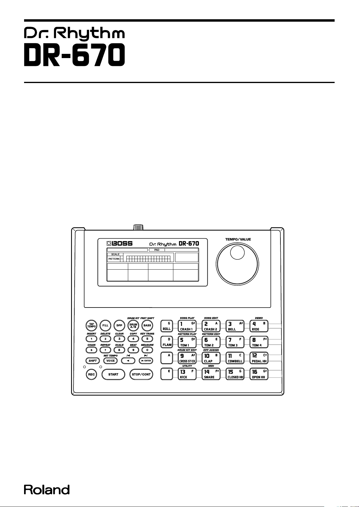
LOCATION OF CONTROLS PARTS LIST
No. Part Code Part Name
1 G2817161 TOP CASE
2 G2567111 DISPLAY COVER
3 F5029411 LCD LMD-STC2K0802DRG
4 F2477101 DR-KNOG GT-3
5 02671212 ROTARY ENCODER EVE GB1 F15 24B
6 G2567112 RUBBER SWITCH for PAD
7 02564267 PRESSURE SHEET SENSOR
8 F5029131 LED (RED) L-1394ID
9 F5029132 LED (GREEN) L-1394GD
10 13429825 MIDI CONNECTOR YKF51-5054 2PZ
11 F3449120 6.5MM JACK HTJ-064-10D
12 F3449106 6.5MM JACK HTJ064-10I
13 F3449401 3.6MM JACK HTJ-035-09DB
14 01340412 P R-KNOB SF-A BLK/LCG
15 01676523 9M/M ROTARY POT. RK09K12A0 10KAx2
16 F3159109 SWITCH(SLIDE) HSW-2022-01
17 13449717 ADAPTOR JACK HEC2392-01-150
18 G2817159 BOTTOM CHASSIS
4
Page 5

Aug.2001 DR-670
LOCATION OF CONTROLS
fig.panel.eps
2 31
4 5
8
9
11 12 13 14 15
76
10 16 17 18
5
Page 6
Aug.2001 DR-670
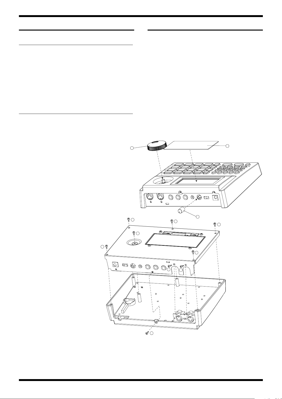
EXPLODED VIEW PARTS LIST EXPLODED VIEW
No. Part Code Part Name Q’ty
1 G2817161 TOP CASE 1
2 G2567112 RUBBER SWITCH for PAD 1
3 02564267 PRESSURE SHEET SENSOR 1
4 F5029411 LCD LMD-STC2K0802DRG 1
5 G2257134 LCD ISOLATION SHEET 1
6 75D462000 MAIN BOARD 1
7 G2817159 BOTTOM CHASSIS 1
8 G2017617 BATTERY CASE 1
9 75D4621000 JACK BOARD 1
10 F2477101 DR-KNOG GT-3 1
11 01340412 P R-KNOB SF-A BLK/LCG 1
12 G2567111 DISPLAY COVER 1
13 F2369405 COATING CLIP 1
No. Part Code Part Name Q’ty
a 40011267 SCREW 3x6 BINDING TAPTITE P ZC 16
b 40011312 SCREW 3x8 BINDING TAPTITE P BZC 12
c 40012534 SCREW 3x6 BINDING TAPTITE S BZC 1
d 40019123 SCREW 3x8 BINDING TAPTITE S BZC 1
fig_bunkai-1.eps
10
b
b
b
b
b
b
11
b
12
b
6
d
Page 7
Aug.2001 DR-670
fig_bunkai-2.eps
13
a
a
a
a
a
a
a
9
8
7
a
a
3
2
a
a
a
a
a
a
6
a
5
4
b
b
c
1
b
b
7
Page 8
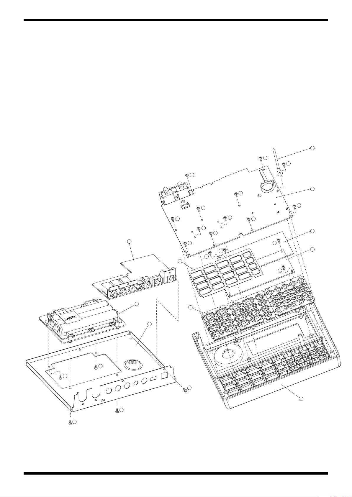
Aug.2001 DR-670
PARTS LIST
fig.part1e
SAFETY PRECAUTIONS:
The parts marked have
safety-related characteristics. Use
only listed parts for replacement.
NOTE: The parts marked # are new. (initial parts)
fig.part2e
NOTE: Consider about the natural environment carefully before through the old lithium battery away when you exchange to the new one.
MB -> MAIN BOARD ASSY, JB -> JACK BOARD ASSY
CASING
# G2567111 DISPLAY COVER 1
# G2817161 TOP CASE 1
CHASSIS
# G2817159 BOTTOM CHASSIS 1
KNOB, BUTTON
# F2477101 DR-KNOG GT-3 1
01340412 P R-KNOB SF-A BLK/LCG 1
# G2567112 RUBBER SWITCH for PAD 1
SWITCH
# F3159109 SWITCH(SLIDE) HSW-2022-01 SW1 on JB 1
SAFETY PRECAUTIONS:
The parts marked have safety-related characteristics. Use only listed parts for replacement.
Failure to completely fill the above items with correct number and description will result in delayed or even
undelivered replacement.
QTY PART NUMBER DESCRIPTION MODEL NUMBER
Ex. 10 22575241 Sharp Key C-20/50
15 2247017300 Knob (orange) DAC-15D
JACK, EXT TERMINAL
DISPLAY UNIT
PCB ASSY
IC
F3449401 HTJ-035-09DB 3.6MM JACK JK5 on JB 1
# F3449120 HTJ-064-10D 6.5MM JACK JK4 on JB 1
F3449106 HTJ064-10I 6.5MM JACK JK2, JK3 on JB 2
13429825 YKF51-5054 2PZ MIDI CONNECTOR JK1 on MB 1
13449717 HEC2392-01-150 ADAPTOR JACK JK1 on JB 1
# F5029411 LCD LMD-STC2K0802DRG INC. WIRING A2001H02-14P 1
NOTE: Replacement LCD LMD-STC2K0802DRG should be made on a unit base.
# 75D4620000 MAIN BOARD ASSY 1
75D4621000 JACK BOARD ASSY INC. WIRING A2001H02-8P 1
# 02564290 UPD703106AGJ-054-UEN IC (CPU) IC4 on MB 1
01340789 BU9480F IC (D/A CONVERTER) IC13 on MB 1
01906156 S-8520E33MC-BJS-T2 IC (DC-DC REGULATOR) IC11 on MB 1
01783123 LH28F400BVE-BL85 IC (FLASH MEMORY/BLANK) IC5 on MB 1
# 02564289 LC24134B-UF2 IC (GATE ARRAY) IC3 on MB 1
# F5229806 MX23L6410TC-12 IC (MASK ROM) IC2 on MB 1
# F5289604 A62S6316-55S IC (SRAM) IC7 on MB 1
F5259701 TC74HC04AFN IC (CMOS) IC1 on MB 1
15249104 TC7S04F(TE85L) IC (CMOS) IC9 on MB 1
15259885 TC7S32F(TE85L) IC (CMOS) IC8 on MB 1
15189209 BA15218 IC (OP AMP) IC1 on JB 1
# 02346123 NJM4556AD IC (OP AMP) IC2 on JB 1
00458034 TC75S51F TE85R IC (OP AMP) IC12 on MB 1
15289124 PC-400 IC (PHOTO COUPLER) IC6 on MB 1
15199955 M51957BFP IC (RESET IC) IC10 on MB 1
TRANSISTOR
15119132 2SA1015-GR(TPE2) TRANSISTOR Q5 on JB 1
15129113 2SC1740SR TRANSISTOR Q1 on JB 1
# 02567101 2SJ278 TRANSISTOR Q2 on MB 1
15329518 DTA114TKAT146 TRANSISTOR Q3, Q4 on MB 2
15129204 DTC343TS TP TRANSISTOR Q2, Q3, Q4, Q6 on JB 4
8
Page 9

Aug.2001 DR-670
TRANSISTOR
00898201 RN2421(TE85L) TRANSISTOR Q1 on MB 1
DIODE
F5019203 1N4004 DIODE D1, D2 on JB 2
15339119T0 1SS-352 DIODE D1, D3 on MB 2
# 02783023 RB500V-40 DIODE D4 on MB 1
01780045 RB051L-40 SCHOTTKY DIODE D2 on MB 1
15019126 1SS133 T-77 SWITCHING DIODE D3, D4 on JB 2
15339108 DA204K T146 DIODE ARRAY DA12, DA13 on MB 2
15339109 DAP202K T146 DIODE ARRAY DA1, DA2, DA3, DA4, DA5, DA6, DA7, DA8,
DA9, DA10, DA11
# F5029132 L-1394GD LED (GREEN) LED2 on MB 1
# F5029131 L-1394ID LED (RED) LED1 on MB 1
RESISTOR
F5429385 100K OHM F RANK (1%) CHIP RESISTOR R42 on MB 1
# F5429411 1MF 1% CHIP RESISTOR R35 on MB 1
# F5429346 3.3KF 1% CHIP RESISTOR R25 on MB 1
# F5429376 39KF 1% CHIP RESISTOR R56 on MB 1
# F5429349 4.7KF 1% CHIP RESISTOR R24 on MB 1
# F5429480 4.7MK 1% CHIP RESISTOR R38 on MB 1
00566867 RPC05T 100 J MTL.FILM RESISTOR R2, R37 on MB 2
00567023 RPC05T 101 J MTL.FILM RESISTOR R6, R64, R65, R66 on MB 4
00567156 RPC05T 102 J MTL.FILM RESISTOR R4 on MB 1
00567289 RPC05T 103 J MTL.FILM RESISTOR R1, R5, R8, R9, R22, R28, R36 on MB 7
00567412 RPC05T 104 J MTL.FILM RESISTOR R27, R29, R30, R31, R33, R34, R39, R43, R44, R45,
R47, R50, R51, R52, R53, R54, R59, R60, R61, R62
on MB
00567034 RPC05T 121 J MTL.FILM RESISTOR R7 on MB 1
00567045 RPC05T 151 J MTL.FILM RESISTOR R63 on MB 1
00567434 RPC05T 154 J MTL.FILM RESISTOR R26, R32, R46, R57 on MB 4
00567056 RPC05T 181 J MTL.FILM RESISTOR R58 on MB 1
00566934 RPC05T 330 J MTL.FILM RESISTOR R3 on MB 1
00566967 RPC05T 470 J MTL.FILM RESISTOR R10, R11, R12, R13, R14, R15, R16, R17, R18, R19,
R20, R21 on MB
00567245 RPC05T 472 J MTL.FILM RESISTOR R23 on MB 1
00567378 RPC05T 473 J MTL.FILM RESISTOR R48, R49 on MB 2
13749797T0 SR25TRE 102 J RESISTOR R11, R12, R23, R24, R26, R29 on JB 6
13749821T0 SR25TRE 103 J RESISTOR R1, R3, R4, R8, R9, R10, R16, R20, R21, R22 on JB 10
13749845T0 SR25TRE 104 J RESISTOR R14, R27, R33, R34, R35 on JB 5
13749823T0 SR25TRE 123 J RESISTOR R5, R17 on JB 2
13749757T0 SR25TRE 220 J RESISTOR R30, R32 on JB 2
13749805T0 SR25TRE 222 J RESISTOR R2 on JB 1
13749853T0 SR25TRE 224 J RESISTOR R31 on JB 1
13749785T0 SR25TRE 331 J RESISTOR R13, R25 on JB 2
13749837T0 SR25TRE 473 J RESISTOR R6, R7, R18, R19 on JB 4
13749839T0 SR25TRE 563 J RESISTOR R15, R28 on JB 2
F5419707 CRN34 101J RESISTOR ARRAY RA13, RA14 on MB 2
# F5419717 CRN34 560J RESISTOR ARRAY RA1, RA2, RA3, RA4, RA5 on MB 5
F5419715 CRN34 680J RESISTOR ARRAY RA7, RA8, RA9, RA11 on MB 4
# F5419718 YC-15 103 J RESISTOR ARRAY RA6, RA10, RA12 on MB 3
11
20
12
POTENTIOMETER
CAPACITOR
01676523 RK09K12A0 10KAx2 9M/M ROTARY POT. VR1 on JB 1
# F5369602 0.33/50V
F5367542 10/16V
F5367546 100/16V
F5367545 47/16V
13519621M0 1H101K5 CERAMIC CAPACITOR C30, C31, C35, C36 on JB 4
13519628 DD104-989B331K50 CERAMIC CAPACITOR C15, C27 on JB 2
13519617M0 ECCR1H470J5 CERAMIC CAPACITOR C6, C8, C19, C20 on JB 4
01674556 ECJ1VB1H472K CERAMIC CAPACITOR C60, C61 on MB 2
13519623M0 ECKR1H151KB5 CERAMIC CAPACITOR C17, C29 on JB 2
13519627M0 ECKR1H271KB5 CERAMIC CAPACITOR C16, C28 on JB 2
13519631M0 ECKR1H561KB5 CERAMIC CAPACITOR C14, C26 on JB 2
01675167 GRM39CH100D50PT CERAMIC CAPACITOR C14, C19 on MB 2
01675190 GRM39CH220J50PT CERAMIC CAPACITOR C68, C69, C70, C71, C72, C73, C74, C75, C76, C77,
01675312 GRM39CH221J50PT CERAMIC CAPACITOR C39, C40, C41, C42, C43, C48, C49, C50, C51, C52,
00567978 GRM39F104Z25PT CERAMIC CAPACITOR C2, C3, C6, C8, C9, C11, C12, C13, C15, C16, C17,
# F3519652 0.1U CHEMICAL CAPACITOR C3, C37, C38 on JB 3
ALUMINIUM ELECTROLYTIC CAPACITOR
ALUMINIUM ELECTROLYTIC CAPACITOR
ALUMINIUM ELECTROLYTIC CAPACITOR
ALUMINIUM ELECTROLYTIC CAPACITOR
C38 on MB 1
C4, C7, C27 on MB 4
C44, C46 on MB 2
C53, C62 on MB 2
C78, C79, C80 on MB
C55, C56, C57, C58, C59, C63, C64, C65, C66, C67
on MB
C18, C20, C21, C22, C23, C24, C25, C26, C28, C29,
C30, C31, C32, C33, C34, C35, C36, C37, C45, C47,
C54 on MB
13
20
32
9
Page 10

Aug.2001 DR-670
CAPACITOR
# 13629150 100/16V CHEMICAL CAPACITOR C1, C2 on JB 2
F3629700 10/16V (H=7MM) CHEMICAL CAPACITOR C7, C10, C11, C12, C13, C18, C21, C23, C24, C25,
C34, C39 on JB
# F3629504 47/16V CHEMICAL CAPACITOR C4, C5, C32, C33 on JB 4
13549313M0 ECQ-B1H472KF3 POLYEST CAPACITOR C9, C22 on JB 2
INDUCTOR, COIL, FILTER
# F2449218 SLF12575T151M1R5 150UH COIL L5 on MB 1
# F2449219 SLF7045T-4R7M2R0 4.7UH COIL L6 on MB 1
# F5409116 BCB809535-600 EMI FILTER L1, L2, L3, L4, L5, L6 on JB 6
# F5409115 MB-20129-0600NR EMI FILTER L1, L2, L3, L4, L7 on MB 5
CRYSTAL, RESONATOR
# F5299114 HC-49SM 5MHZ CRYSTAL X1 on MB 1
12
ENCODER
CONNECTOR
WIRING, CABLE
PICKUP, SENSOR
SCREW
PACKING
02671212 EVE GB1 F15 24B ROTARY ENCODER EN1 on MB 1
# F3439174 CONNECTOR A2001WV2-2P CN1 on JB 1
# F3439173 CONNECTOR A2001WV2-8P CN3 on MB 1
# F3439175 CONNECTOR A2001WV2-14P CN2 on MB 1
# G3487424 WIRING 2P L=230 A2001H02-2P CN1 on JB to BATTERY CASE 1
# 02564267 PRESSURE SHEET SENSOR 1
40011267 SCREW 3x6 BINDING TAPTITE P FE ZC 16
40012534 SCREW 3x6 BINDING TAPTITE S FE BZC 1
40011312 SCREW 3x8 BINDING TAPTITE P BZC 12
40019123 SCREW 3x8 BINDING TAPTITE S BZC 1
# G260721301 PACKING CASE 1
# G2237618 PAD BATTERY 1
# G2237615 PAD L 1
# G2237617 PAD R 1
MISCELLANEOUS
ACCESSORIES (STANDARD)
G2017617 BATTERY CASE 1
G2027602 BATTERY COVER 1
G2177306 BATTERY TERMINAL (-) 1
G2177305 BATTERY TERMINAL (+) 1
G2177304 BATTERY TERMINAL (+/-) 2
# F2369405 COATING CLIP 1
12569249 CR2032 220MAH/3V LITHIUM BATTERY 1
# G2147127 DC JACK HOLDER 1
# G2357119 FOOT 4
# G2257134 LCD ISOLATION SHEET 1
# H2369430 LED SPACER LEDS-1.5 2
# F2569111 LITHIUM BATTERY HOLDER TACT383-009 BT1 on MB 1
# G2257133 MAIN BOARD SHIELD SHEET 1
# G2147126 PHONE JACK HOLDER 1
# G6017448 OWNER’S MANUAL SET JAPANESE 1
# G6017449 OWNER’S MANUAL SET ENGLISH 1
********
NOTE : The above part (ALKALINE DRY BATTERY LR6) does not supply as replacement parts,because it is options.
40232389 WARRANTY CARD (JAPAN ONLY) 1
ALKALINE DRY BATTERY LR6 (AA) TYPE
6
10
Page 11

Aug.2001 DR-670
IDENTIFYING THE VERSION NUMBER
While holding down [REC] and [6] buttons, turn on the DR-670’s power.
The following message will appear on the LCD display.
The mask CPU (IC4 on Main Board) version is shown.
The flash memory (IC5 on Main Board) can be updated from the external MIDI
device.
“100A” means Version 1.00A.
fig.vere
|
|
|
|
--- MASK CPU VERSION
|
|
--- FLASH ROM VERSION
SAVEING USER DATA & RELOADING SAVED DATA
Saving your DR-670 data in a MIDI sequencer or another DR-670 is known as
“Bulk Dump.”
Conversely, returning data saved in the MIDI sequencer back to the DR-670, or
receiving data transmitted from another DR-670 is called “Bulk Load.”
Perform Bulk Dump and Bulk Load in the MIDI mode.
To select the MIDI mode, stop the performance first.
Then, hold down [SHIFT] and press Key pad [14](MIDI) buttons.
fig.09-02a_e
Holding down
fig.09-03
Saving the DR-670’s data (Bulk Dump)
fig.09-11e
MIDI OUT
Transmit device
(DR-670)
To carry out Bulk Dump, select the MIDI mode (by holding down [SHIFT] and
pressing Keypad [14] (MIDI) buttons) and proceed as follows:
1. Press [ ] and [ ] buttons to select “TX BULK.”
fig.09-12
2. Select the data you want to transmit by rotating the [TEMPO/VALUE]
control.
ALL: All of the DR-670’s data
SEQ: Data recorded in User patterns and Songs
UTIL: Utility mode, MIDI mode, and DPP assignment data
KIT: All of the User drum kits
3. Press [START] button.
Bulk Dump starts, and the Tempo indicator lights up.
After a few moments, the Temp indicator will go out and Bulk Dump is
completed.
* If you select “ALL” for Bulk Dump, the memory of the receiving device may
become full and further dumping may be rejected.
If this occurs, select the SEQ, UTIL or KIT option and repeat Bulk Dump.
Receive device
(MIDI Sequencer etc.)
MIDI IN
Setting the Device ID
Patterns, drum kits and other device-specific data are transmitted and received
as “Exclusive messages” during Bulk Dump or Bulk Load. You must assign
correct device identification numbers (Device IDs) so that the devices can
recognize them.
Set device ID by performing the following operation in the MIDI mode.
1. Press [ ] and [ ] buttons and select “DEV.”
2. Rotate the [TEMPO/VALUE] handle and set the device ID.
fig.09-10
Setting values: 17 to 32
Returning Saved Data to the DR-670 (Bulk Load)
fig.09-13e
MIDI OUT
Transmit device
(MIDI Sequencer etc.)
To carry out Bulk Load, select the MIDI mode (by holding down [SHIFT] and
pressing Keypad [14] (MIDI) buttons) and proceed as follows:
1. Press [ ] and [ ] buttons to select “RX BULK.”
fig.09-14
2. Transmit the saved data from the connected MIDI device.
Bulk Load starts, and the REC indicator lights up.
After a few moments, the REC indicator will go out and Bulk Load is
completed.
Receive device
MIDI IN
(DR-670)
11
Page 12

Aug.2001 DR-670
TEST MODE
Equipment items
1.AC Adaptor PSA series
2.MIDI Cable
3.Foot Switch x2pcs. (FS-5U x2)
4.Foot Switch Cord PCS-31 (Stereo Phone Jack <—> Phone Jack x2)
5.Oscilloscope
6.Noise Meter
7.Headphones
8.Monitor Amp (Stereo)
Test items
1.Version / Power Voltage
2.Lithium Battery
3.Gate Array
4.Mask ROM
5.SRAM
6.Flash Memory
7.MIDI
8.LED
9.LCD
10.Switch
11.Pad
12.Encoder
13.Foot SW
14.Output
15.Factory Reset
16.Normal operation check
17.PAD test
18.Battery operation check
Cautions: The Test programs are executed in the flash memory.
Items 1 to 15 are executed in the Test mode.
During these tests, all user memory data are LOST.
Save your data by Bulk Dump before starting the tests.
Preparation
Selecting Test Items
You can select the desired test item by rotating the Encoder control.
1. Version/Power Voltage
fig.1-1
|
|
|
|
|
|
|
|
|
Power Voltage
|
|
|
Version A
"T-B": Power Voltage OK
"NG": Power Voltage NG
Power Voltage (x100)
Version A: CPU Mask Program Version (w/minor version)
Version B: Flash program Version (w/minor version)
ex:
Power Voltage
830: 8.30 V
Version A/B
123D: Ver.1.23D
100C: ver.1.00C
Test: Supply 9.0 V ± 0.1 V to TEST DC IN JACK, and check if “T-B” is
displayed on the LCD.
The source voltage supplied to the DR-670’s main board (via the CN3
connector with +9V pin 1 and GND pin 2) is measured by the CPU and
indicated on the display.
When 9.0V power is supplied to the DC IN jack, the Power Voltage of 750 to
893 (7.50 to 8.93V) is indicated due to a slight voltage drop in the jack board
circuit or a device error.
The LCD display shows the “T-B” within this range.
A precise 9.0-volt reading may not be output due to the PSA series adapter
used for the test.
However, you can perform other tests normally even if power voltage “NG” is
shown.
2. Lithium Battery
fig.2-1e
|
|
Version B
Power supply : Plug the PSA series Power Adapter (optional) into the DR-670.
FOOT SW : Connect two FS-5Us via PCS-31.
Set the POLARITY switch to “Jack side” on each FS-5U.
MIDI : Loop the IN and OUT terminals.
Selecting the Test Mode
While holding down [REC] and [6] buttons, turn on the DR-670’s power.
The power voltage and version A/B will appear on the display.
|
|
|
|
|
The Lithium battery voltage is shown.
|
"OK" (Normal) or "NG" (Low voltage) is displayed.
Operation : You can select another test by rotating the Encoder control.
Test : Make sure that “OK” is displayed.
“OK” means that the current Lithium battery voltage is 2.70 to
3.70V (270 to 370).
You can select another test by rotating the Encoder control
regardless of the voltage test result.
12
Page 13

Aug.2001 DR-670
3. Gate Array
fig.3-1
Operation : Press [START] button to start the Gate Array test.
If the result is “OK,” you can select another test by rotating the
Encoder control.
fig.3-2e
If “NG,” the test has failed. You cannot start another test.
|
|
|
|
|
The readout is displayed during error.
|
"OK" (Normal) or "NG" (Test failure) is displayed.
4. Mask ROM
fig.4-1
Operation : Press [START] button to start the Mask ROM test.
If the result is “OK,” you can select another test by rotating the
Encoder control.
fig.4-2e
If “NG,” the test has failed. You cannot start another test.
7. MIDI
fig.7-1
Operation : Press [START] button to start the MIDI test.
If the result is “OK,” you can select another test by rotating the
Encoder control.
If “NG,” the test has failed.
fig.7-2e
You cannot start another test.
|
|
|
|
|
The error code is displayed.
|
"OK" (Normal) or "NG" (Test failure) is displayed.
Error codes 0000 to 0007 : Receive status error
1000 : Tx Buffer Full Error
2000 : Verify Error
3000 : Data Number Error (Too much data exists.)
4000 : Rx Buffer Full Error
5000 : Data Number Error (Very little data exists.)
8. LEDs
fig.8-1
|
|
|
|
|
The error count is displayed during error.
|
"OK" (Normal) or "NG" (Test failure) is displayed.
5. SRAM
fig.5-1
Operation : Press [START] button to start the SRAM test.
If the result is “OK,” you can select another test by rotating the
Encoder control.
If “NG,” the test has failed.
fig.5-2e
You cannot start another test.
|
|
|
|
|
The error address is displayed during error.
|
"OK" (Normal) or "NG" (Test failure) is displayed.
6. Flash Memory
fig.6-1
Operation : Press [START] button to start the LED test.
You can select another test by rotating the Encoder control.
Test : The red and green LEDs light alternately each time you press
[START] button.
Visually check the lit LED positions and their brightness. (A click
must be heard from OUTPUT JACK.)
9. LCD Panel
fig.9-1
Operation : Press [START] button to start the LCD Panel test.
You can select another test by rotating the Encoder control.
Test : Divide the display dots into 16 groups, and check the on/off
switching of each group.
The dot groups are switched and displayed one after the other
when you press [START] button.
When the 16-th group of dots come on, all dots turn on when you
press [START] button.
Then, all dots go out when you press [START] button again.
Visually check each one for a missing dots, and uneven or
intensity error display. (A click must be heard from OUTPUT
JACK.)
10. Switches
fig.10-1e
Operation : Press [START] button to start the Flash Memory test.
If the result is “OK,” you can select another test by rotating the
Encoder control.
fig.6-2e
If “NG,” the test has failed. You cannot start another test.
|
|
|
|
|
The checksum result is displayed.
|
"OK" (Normal) or "NG" (Test failure) is displayed.
Operation :
|
|
|
|
|
"ON," "OFF" or "NG" is displayed.
|
The name and status of the operated switch are shown.
The switch “ON” or “OFF” status appears when you turn it on or off.
Turn all switches on and off one after the other, and make sure
that their correct names and “ON” or “OFF” state appear.
If you operate two switches simultaneously, “NG” is displayed.
You can select another test by rotating the Encoder control.
13
Page 14

Aug.2001 DR-670
11. Pad
fig.11-1e
|
|
|
|
|
|
Your padding force is indicated within 0 to 100
"NG" is displayed.
|
The pressed pad is shown.
Operation : When a pad name is displayed, press it.
Your padding force will be shown within 0 to 100.
The test starts from the left upper end [G] pad.
Press the pads one after the other, and check their display values.
Check the following points.
1. The display value increases or decreases according to your
padding force.
2. The display value reaches the limit (“100”) when you press
strongly.
If you press two pads simultaneously, “NG” is displayed.
You can select another test by rotating the Encoder control.
12. Encoder
fig.12-1e
|
|
|
|
|
Accumulation result is shown.
|
The readout increases or decreases by 1
when you rotate the control slowly.
Operation : 1. Press [START] button to start the Encoder test.
2. Check the display by rotating the Encoder control.
The value must increase when you rotate the control clockwise
(CW), and decrease when rotate it counterclockwise (CCW).
3. Press [STOP] button to stop the Encoder test.
You can select another test by rotating the Encoder control.
13. Foot Switch
fig.13-1e
|
|
|
|
|
"ON," "OFF" or "NG" is displayed.
|
The name and status of the operated switch are shown.
Operation : The name and “ON” or “OFF” status of foot switch appear when
you operate it.
Operate the foot switches one after the other, and check for their
name and on/off status appear.
If you operate two switches simultaneously, “NG” is displayed.
You can select another test by rotating the Encoder control.
14. Output
fig.14-1
|
|
|
|
|
Rch: "SQR-", "SIN-", "MUTE"
|
Lch: "SQR+", "SIN+", "MUTE
Operation : (1) [1] button 1k Hz square waves are output on L channel, but
they are delayed 90 degrees on R channel.
(2) [2] button 1k Hz sine waves are output in the same phase on
both L and R channels.
(3) [3] button Mute
(1) Check the waveforms and their phases.
(2) Check the waveforms. The OUTPUT level of both L and R
channels must be +3 dB +/- 1 dB (FLAT) when the Amplitude
control is at the “MAX” position.
(3) Shake the DR-670 and make sure that no abnormal sounds are
heard.
* Accurate frequency of output waveforms: 1.0173k Hz
15. Factory Reset
fig.15-1
Operation : Press [START] button to start “Factory Reset.”
16. Normal operation check
Turn on the DR-670’s power again, and press [START] button.
Check the pattern playback sounds.
Rotate the sound control and make sure that the sound level changes smoothly.
Press [STOP] button to stop playback.
Connect the headphones and check the playback sound and volume change of
the pattern with the operation mentioned above.
Place the control at the ‘MAX’ position, and measure the residual noise using a
noise meter.
(The noise level of both L and R channels must be -85 dBm (JIS-A).)
Increase the sound level of the playback amp, and check for sound control noise.
Place the control at the ‘MAX’ position, and check for noise and howling.
17. PAD test
Press [BASS] button to select the BASS sound mode.
Beat each pad by changing the force, and make sure that the base sound level
changes.
Below indicates failure:
• No sound is output.
• Sound is too short.
• Sound continues without stopping.
• Noise is generated.
18. Battery operation check
Unplug the AC adapter from the DR-670, and insert six dry cells into the
battery box.
Turn on the DR-670’s power and make sure that it operates normally.
If the output voltage of the six dry cells is below 7 Vdc, the “DRY BATTERY
LOW” message is displayed.
14
Page 15

Aug.2001 DR-670
RESET TO DEFAULT FACTORY SETTINGS (FACTORY RESET)
Caution : When Factory Reset is carried out, all data stored in the DR-670 are
LOST.
The unit is returned to the settings in effect when it was shipped
from the factory.
If you already have important data stored in the DR-670, save it to
an external MIDI device (such as a MIDI sequencer) by Bulk Dump
before starting Factory Reset.
fig.00-05
1
Operation
Cautions : All user data are LOST during updating.
Before starting updating, save your data by following the “Saving
or Loading Data” procedure.
Data updating takes approximately 10 minutes.
1. Save the user data by following the “Saving or Loading Data” procedure.
2. While holding down [REC] and [0] buttons, turn on the DR-670’s power.
The following message will appear.
fig.up-1e
|
|
|
|
--- MASK CPU VERSION
“100A” means Version 1.00A.
Only the Flash Memory contents can be updated from the external MIDI
device.
3. Insert the “SMF Update” disk into the drive of the MIDI sequencer, and
start updating.
4. The red LED will flash or light when updating starts.
fig.up-2
|
|
--- FLASH ROM VERSION
2,31
1. While holding down [REC] and [STOP/CONT] buttons, turn on the DR670’s power.
fig.00-06
2. Press [ ] button.
The “FCT RST OK?” confirmation message appears.
fig.00-07
To cancel Factory Rest, just turn off the power.
3. Press [ ] button once more.
Factory Reset is completed, and “DONE” appears.
4. Turn off the DR-670’s power.
PROCEDURE FOR UPDATING THE SOFTWARE
BLKn : The block number being received (“n” is 1 to 8).
ssss : The checksum of each block. It shows the checksum of the
5. Block reception is completed when the following message appears:
fig.up-3
6. Turn off the DR-670’s power.
7. Turn on the DR-670’s power again without pressing any key.
fig.up-4
8. Load the saved user data.
Note: When the following is displayed in Bulk Load with products of serial
previously received block.
aaaa : Checksum of all blocks
ssss : Checksum of the last block
* Check the “aaaa” checksum value of all blocks.
When the following message appears, press [ ] button to
initialize the user data.
numbers earlier than ZO95000, remove the 10/16V (C5) capacitor on
the main board. (C5 part will not be implemented.)
Then perform Bulk Load again.
Equipment items
1. MIDI Sequencer
2. Update SMF 2HD Disk Set (#17041070)
Connection
Plug one end the MIDI cable into MIDI IN of the DR-670, and the other end
into MIDI OUT of the MIDI sequencer.
15
Page 16

Aug.2001 DR-670
ERROR MESSAGE LIST
Incorrect operation or operation failure causes an error message to appear.
The following lists the possible error messages and actions to be taken.
fig.10-01
The DR-670’s dry cells (batteries) are running low.
Use the AC adapter, or replace the cells.
Press [STOP/CLEAR] button to clear the message.
If you continue to use the DR-670 at low voltage, sounds may be distorted or
the unit may not operate correctly.
fig.10-02
The service life of DR-670’s memory backup battery has almost expired.
(This message appears when the power is turned on.)
Replace the battery as soon as possible.
Consult the Roland Service Center for backup battery replacement.
Caution: Although you can clear the message by pressing [STOP/CONT]
button and continue to operate the DR-670, recorded patterns and songs may
be lost when you turn off the power.
fig.10-03
Data stored in the DR-670 has been corrupted.
You need to reset the data. (This message appears when the power is turned on.)
Press [ ] button to restore the factory settings.
fig.10-04
fig.10-07
MIDI Exclusive messages could not be received correctly.
Press [STOP/CONT] button and retry the operation.
fig.10-07a
The system failed to process data as it tried to concurrently process an
abnormally large amount of data.
Press [STOP/CONT] button.
Make sure that the unit is not being forced to handle an excessive amount of
data (in patterns or MIDI message reception) at a time, and try to reduce the
amount of data to be processed.
fig.10-07b
An unidentifiable error has occurred in the system.
Shut down the DR-670 immediately.
Memory is full.
No more patterns or songs can be recorded.
Press [STOP/CONT] button.
To continue recording, first delete unnecessary patterns or songs.
fig.10-04a
The number of patterns recorded in the song exceeded 250.
Press the [STOP/CONT] button.
You cannot record any further to the song currently being edited. To continue,
create a new song, then use Song Chain.
fig.10-05
When trying to copy or clear a pattern or song, no data to be copied or cleared
has been recorded in the copy source and pattern and song.
Check the pattern and song numbers of the copy source or data to be cleared.
fig.10-05a
A MIDI Active Sensing error has occurred.
The devices or cables connected to the MIDI IN port have failed.
Check the connected devices and cables.
fig.10-06
The DR-670’s processing capacity was exhausted as it received too much MIDI data.
Press [STOP/CONT] button.
Reduce the amount of MIDI data and send again from the MIDI device to the
DR-670.
fig.10-07c
Reception of data during Bulk Load was cancelled before the operation was
completed.
Press the [STOP/CONT] button, then try carrying out Bulk Load again.
16
Page 17

Aug.2001 DR-670
17
Page 18

Aug.2001 DR-670
BLOCK DIAGRAM
fig.block
MIDI
OUT
IN
IC6
PHOTO
COUPLER
2/6 IC1
Q3
IC4
CPU
uPD703106
LCD MODULE
GATE ARRAY
IC3
A
ENCODER
IC13
DAC
BU9480
IC2IC1
BA15218 NJM4556
VOLUME
FOOT SW
PHONES
L(MONO)
R
OUTPUT
RED
POWER
ANALOG
1 1
Q4
GREEN
DATA BUS
ADDRESS BUS
IC12
CR2032
SWITCH
4/6 IC1
DC-DC
CONVERTER
VCC_3.3
IC11
Q2
DC IN 9V
BATTERY
JACK BOARD
IC7
SRAM
VCC_3.3
Q1
Vpp
IC5
FLASH MEM
PRESSURE
SENSOR
SW MATRIX
MAIN BOARD
A
18 19
Page 19

Aug.2001 DR-670
CIRCUIT BOARD (MAIN)
fig_circuit board_MAIN-1.eps
20
View from components side
Page 20

Aug.2001 DR-670
fig_circuit board_MAIN-2.eps
View from fiol side
21
Page 21

Aug.2001 DR-670
CIRCUIT DIAGRAM (MAIN)
fig.main
R1
10k
D
L1
MB-201209-0600NR
R6 100
R7
120
SW(FILL)
1 2
DA2
DAP202K
3
SW(2)
1 2
1 2
SW(6)
1 2
DA6
DAP202K
3
SW(REC)
1 2
1 2
SW(0)
1 2
DA10
DAP202K
3
1 2
1 2
SW(>/ENTER)
1312
1110
D1
1SS352
A
WAVE ROM
IC2
12
WA22
A21
13
WA21
A20
11
WA20
A19
14
WA19
A18
15
WA18
A17
2
WA17
+
D3.3
R2
10
R3
33
+
D3.3
R4
1k
65
1
4
3
2
C9
D
SW(DPP)
1 2
DA3
DAP202K
SW(3)
1 2
1 2
SW(7)
1 2
DA7
DAP202K
SW(SHIFT)
1 2
1 2
SW(START)
1 2
DA11
DAP202K
1 2
1 2
SW(STOP/CONT)
IC6
PC400
0.1
1 2
3
3
3
WA15
WA14
WA13
WA12
WA11
WA10
WA9
WA8
WA7
WA6
WA5
WA4
WA3
WA2
WA1
DC
D
SW(DRUM A/B)
1 2
3
1 2
1 2
1 2
3
1 2
1 2
A16
3
A15
4
A14
5
A13
6
A12
7
A11
8
A10
9
A9
10
A8
16
A7
17
A6
18
A5
19
A4
20
A3
21
A2
22
A1
23
A0
1
WORD/BYTE
24
CE
27
OE/OE/DC
36
NC
MX23L6410TC-12
DA4
DAP202K
SW(4)
SW(8)
DA8
DAP202K
SW(VOICE)
O15/A-1
VCC
VCC
GND
GND
GND
GND
46
WA0
44
O14
42
O13
40
O12
35
O11
33
O10
31
O9
29
O8
45
WD7
O7
43
WD6
O6
41
WD5
O5
39
WD4
O4
34
WD3
O3
32
WD2
O2
30
WD1
O1
28
WD0
O0
38
37
48
47
26
25
+
D3.3
98
IC1D
TC74HC04AF
IC1C
TC74HC04AF
IC1B
TC74HC04AF
IC1A
TC74HC04AF
+
D3.3
147
D
C2
0.1
TC74HC04AF
+
D3.3
IC1F
TC74HC04AF
IC1E
TC74HC04AF
4 4
MIDI
JK1
YKF51-5054
L7
MB-201209-0600NR
D
304050
60
25
22
2
24
45
2
IN OUT
45
L3
MB-201209-0600NR
L4
MB-201209-0600NR
SWITCH
3 3
SW(TAP TEMPO)
3
3
2 2
3
15
12
14
1 2
DA1
DAP202K
SW(1)
1 2
1 2
SW(BASS)
1 2
DA5
DAP202K
SW(5)
1 2
1 2
SW(9)
1 2
DA9
DAP202K
1 2
1 2
SW(<)
L2 MB-201209-0600NR
C10
N.I.U
D
PRESSURE SENSOR
PAD(ROLL)
1 2
C39
220p
PAD(FLAM)
1 2
C48
220p
PAD(A)
1 2
1 1
C55
220p
PAD(E)
1 2
C63
220p
PAD1
PAD6
PAD11
PAD16
PAD(CRASH1)
1 2
C40
220p
PAD(TOM1)
1 2
C49
220p
PAD(CROSS ST)
1 2
C56
220p
PAD(KICK)
1 2
C64
220p
PAD2
PAD7
PAD12
PAD17
PAD(CRASH2)
1 2
C41
220p
PAD(TOM2)
1 2
C50
220p
PAD(CLAP)
1 2
C57
220p
PAD(SNARE)
1 2
C65
220p
PAD3
PAD8
PAD13
PAD18
PAD(BELL)
1 2
C42
220p
PAD(TOM3)
1 2
C51
220p
PAD(COWBELL)
1 2
C58
220p
PAD(CLOSED HH)
1 2
C66
220p
PAD4
PAD9
PAD14
PAD19
PAD(RIDE)
1 2
C43
220p
PAD(TOM4)
1 2
C52
220p
PAD(PEDAL HH)
1 2
C59
220p
PAD(OPEN HH)
1 2
C67
220p
DDD D D
PAD5
PAD10
PAD15
PAD20
PAD1
PAD2
PAD3
PAD4
PAD5
PAD6
PAD7
PAD8
PAD9
PAD10
PAD11
PAD12
PAD13
PAD14
PAD15
PAD16
PAD17
PAD18
PAD19
PAD20
A
B
GATE ARRAY
LC24134B-UF2
IC3
77
WD7
WD6
WD5
WD4
WD3
WD2WA16
WD1
WD0
WA22
WA21
WA20
WA19
WA18
WA17
WA16
WA15
WA14
WA13
WA12
WA11
WA10
WA9
WA8
WA7
WA6
WA5
C13
0.1
+
D3.3
R26 150k
R27 100k
R29 100k
R30 100k
R31 100k
R32 150k
R33 100k
R34 100k
R39 100k
R45 100k
R46 150k
R47 100k
R51 100k
R52 100k
R54 100k
R57 150k
R59 100k
R60 100k
R61 100k
R62 100k
WA4
WA3
WA2
WA1
WA0
34
PAD1
PAD2
PAD3
PAD4
PAD5
PAD6
PAD7
PAD8
PAD9
PAD10
PAD11
PAD12
PAD13
PAD14
PAD15
PAD16
PAD17
PAD18
PAD19
PAD20
R64 100
R65 100
R66 100
D
56
IC1G
12
LDA
LDE
LD0
LD1
LD2
LD3
LD4
LD5
LD6
LD7
R40
N.I.U
R55
N.I.U
76
75
74
70
69
68
67
107
106
105
104
103
102
101
100
99
98
97
96
95
94
93
92
89
88
87
86
85
84
83
66
48
47
46
45
44
43
52
51
50
49
118
135
3
79
39
119
136
4
80
40
120
137
5
81
41
121
138
6
82
42
71
RA13 CRN34101J
RA14 CRN34101J
1 8
2 7
3 6
4 5
1 8
2 7
3 6
4 5
+
D3.3
R41
N.I.U
D
WD7
WD6
WD5
WD4
WD3
WD2
WD1
WD0
WA22
WA21
WA20
WA19
WA18
WA17
WA16
WA15
WA14
WA13
WA12
WA11
WA10
WA9
WA8
WA7
WA6
WA5
WA4
WA3
WA2
WA1
WA0
XWOE
SWIN5
SWIN4
SWIN3
SWIN2
SWIN1
SWIN0
SWOUT3
SWOUT2
SWOUT1
SWOUT0
ANAI0
ANAI1
ANAI2
ANAI3
ANAI4
ANAI5
ANAI6
ANAI7
ANAI8
ANAI9
ANAI10
ANAI11
ANAI12
ANAI13
ANAI14
ANAI15
ANAI16
ANAI17
ANAI18
ANAI19
XDRST
LCD063LCD162LCD261LCD360LCD4
LD0
LCD558LCD6
LCD7
LCDE
59
57
56
64
LDE
LD4
LD5
LD6
LD1
LD2
LD3
LD7
C71
C70
C69
C68
22p
22p
22p
22p
D
R58
D
180
R63
150
D
CLKOUT
XDREQ2
XDACK2
XDREQ1
XDACK1
XDREQ0
XDACK0
XENCINT
LCDA
29
65
LDA
C72
C73
22p
22p
LED1
L-1394ID
LED2
L-1394GD
CD15
CD14
CD13
CD12
CD11
CD10
CD9
CD8
CD7
CD6
CD5
CD4
CD3
CD2
CD1
CD0
CA3
CA2
CA1
CA0
XCS
XRD
XWR
XWAIT
SYSCLK
CLKIN
SELA
SELB
XSWINT
FOOT0
FOOT1
ENCA
ENCB
LRCLK
BCK
MCK
XRST
ANAO0
ANAO1
ANAO2
ANAO3
ANAO4
VDD7
VDD6
VDD5
VDD4
VDD3
VDD2
VDD1
VDD0
VSS10
VSS9
VSS8
VSS7
VSS6
VSS5
VSS4
VSS3
VSS2
VSS1
VSS0
XLCDBSY
BG104 GA
12
SD
C74
22p
12
24
23
22
21
20
17
16
15
14
13
12
11
10
9
8
7
142
141
140
139
114
115
113
116
110
111
112
128
129
130
131
132
133
124
125
122
123
33
34
31
32
28
27
25
26
30
117
134
2
78
38
144
126
109
90
73
54
37
18
143
127
108
91
72
55
53
36
35
19
1
D3.3
C75
22p
+
D3.3
3 1
+
D3.3
3 1
LCDBSY#
+
C76
22p
WREADY#
DACK2#
WSET#
DACK1#
16SAMPLE#
DACK0#
SWINT#
ENCINT#
2
2
D15
D14
D13
D12
D11
D10
D9
D8
D7
D6
D5
D4
D3
D2
D1
D0
A4
A3
A2
A1
CS3#
RD#
WAIT#
SYSCLK
SELA
SELB
FOOT0
FOOT1
ENCA
ENCB
AIN0
AIN1
AIN2
AIN3
AIN4
D3.3
C16
C15
0.1
0.1
D
C22
0.1
TO LCD
D
A2001WV2-14P
C77
C78
22p
22p
Q3
DTA114TKA
RED#
Q4
DTA114TKA
GREEN#
WR#
10
11
12
13
14
1
2
3
4
5
6
7
8
9
LRCLK
BCLK
SDATA
+
C17
0.1
C23
0.1
CN2
C18
0.1
C24
0.1
1
2
3
4
5
6
7
8
9
10
11
12
13
14
B
C
D
E
FLASH
28F400BVE-BL85
CS0#
WR#
RD#
+
WR#
RD#
UBE#
LBE#
CS1#
R25
3.3k(1%)
R36
10k
BT1
C60
R50
A18
A17
A16
A15
A14
A13
A12
A11
A10
A9
A8
A7
A6
A5
A4
A3
A2
A1
VPPON#
A16
A15
A14
A13
A12
A11
A10
A9
A8
A7
A6
A5
A4
A3
A2
A1
R24
4.7k(1%)
7
2
1 2
100k
D
17
A17
48
A16
1
A15
2
A14
3
A13
4
A12
5
A11
6
A10
7
A9
8
A8
18
A7
19
A6
20
A5
21
A4
22
A3
23
A2
24
A1
25
A0
26
CE
11
WE
28
OE
14
WP
47
BYTE
12
RP
15
RY/BY
+
D3.3
18
19
20
21
24
25
26
27
42
43
44
1
2
3
4
5
6
17
41
40
39
2 4
C21
IC9
0.1
TC7S04F
RESET
VDD
IN
VSS4CAP
IC10
M51957BFP
D3
1SS352
R43
100k
C61
0.0047
IC5
IC7
A15
A14
A13
A12
A11
A10
A9
A8
A7
A6
A5
A4
A3
A2
A1
A0
CE
WE
OE
HB
LB
A62S6316
SRAM
53
OUT
NC1
NC2
NC3
R53
100k
E
49
ADTRG/IP123/P37
50
IP122/P36
51
IP121/P35
52
RXD2/IP120/P34
53
TXD2/IP133/P33
54
SCK2/IP132/P32
55
SI2/IP131/P31
56
1 4
HC-49SM 5M
C47
0.1
D
FOOT0
FOOT1
SO2/IP130/P30
65
SCK1/P45
66
RXD1/SI1/P44
67
TXD1/SO1/P43
68
SCK0/P42
69
RXD0/SIO/P41
70
TXD0/SO0/P40
71
AVDD/AVREF
72
AVSS
73
P77/ANI7
74
P76/ANI6
75
P75/ANI5
76
P74/ANI4
77
P73/ANI3
78
P72/ANI2
79
P71/ANI1
80
P70/ANI0
19
DRQ3/IP103/P07
20
DRQ2/IP102/P06
21
DRQ1/IP101/P05
22
DRQ0/IP100/P04
23
TO00/P03
24
IP001/P02
25
TIO00/IP000/P01
26
PWM0/P00
29
DMAAK3/PBD3
30
DMAAK2/PBD2
31
DMAAK1/PBD1
32
DMAAK0/PBD0
33
TO01/P13
34
IP011/P12
35
TIO10/IP010/P11
36
PWM1/P10
39
TC3/IP113/P27
40
TC2/IP112/P26
41
TC1/IP111/P25
42
TC0/IP110/P24
43
TO02/P23
44
IP021/P22
45
TIO20/IP020/P21
46
NMI/P20
83
P52/TO03
84
P51/IP031
85
P50/IP030/TI030
86
PCM5/SELFREF
60
CKSEL
62
X2
X1
63
X1
61
CVDD
64
CVSS
59
RESET
LRCLK
BCLK
SDATA
5
VIN
1
IN
2
VSS
D
+
D3.3
1
1
2
2
3
3
4
4
5
5
6
6
7
7
CN1
N.I.U
R12 47
R13 47
R14 47
C25
0.1
DA12
DA204K
D3.3
C3
0.1
D
L6
SLF7045T-4R7M2R0(4.7uH)
+
D3.3
R48
47k
+
D3.3
12
3
+
C4
10/16
D
AIN4
AIN3
AIN2
AIN1
AIN0
BATT-1
BATT-2
WREADY#
WSET#
16SAMPLE#
LCDBSY#
VPPON#
LCDRES
DACK2#
DACK1#
DACK0#
SELB
SELA
C19
10P
D
C26
0.1
100/16
R49
47k
D3.3
3
GREEN#
RED#
SWINT#
ENCINT#
16SAMPLE#
D
C14
10P
+
D3.3
C46
BATT-1
+
12
DA13
DA204K
DD
D
EXT
VOUT
IC11
S-8520E33MC-BJS
R42
100k(1%)
2.5V
R56
39k(1%)
D
C80
C79
22p
22p
D D
CPU
PCM1/CLKOUT/BUSCLK
PCT1/UCAS/UWR/UDQM
PCT0/LCAS/LWR/LDQM
PCS6/CS6/RAS6
PCS5/CS5/IORD
PCS4/CS4/RAS4
PCS3/CS3/RAS3
PCS2/CS2/IOWR
PCS1/CS1/RAS1
PCD3/UBE/SDRAS
PCD2/LBE/SDCAS
VSS
VSS
VSS
VSS
VSS
VSS
VSS
9
28
38
48
82
99
113
D
23
Q2
1
2SJ278
4
3
TO JACK BOARD
9V
D
C
114
PAH9/A25
115
PAH8/A24
116
PAH7/A23
117
PAH6/A22
118
PAH5/A21
119
PAH4/A20
120
PAH3/A19
121
PAH2/A18
122
PAH1/A17
123
PAH0/A16
126
PAL15/A15
127
PAL14/A14
128
PAL13/A13
129
PAL12/A12
130
PAL11/A11
131
PAL10/A10
132
PAL9/A9
133
PAL8/A8
136
PAL7/A7
137
PAL6/A6
138
PAL5/A5
139
PAL4/A4
140
PAL3/A3
141
PAL2/A2
142
PAL1/A1
143
PAL0/A0
144
PDL15/D15
1
D14/PDL14
2
D13/PDL13
3
D12/PDL12
4
D11/PDL11
5
D10/PDL10
6
D9/PDL9
7
D8/PDL8
10
D7/PDL7
11
D6/PDL6
12
D5/PDL5
13
D4/PDL4
14
D3/PDL3
15
D2/PDL2
16
D1/PDL1
17
D0/PDL0
90
91
PCM0/WAIT
87
PCM4/REFRQ
88
PCM3/HLDRQ
89
PCM2/HLDAK
92
PCT7/BCYST
93
PCT6/OE
94
PCT5/WE
95
PCT4/RD
96
97
100
PCS7/CS7
101
102
103
104
105
106
107
PCS0/CS0
108
109
110
PCD1/SDCLK
111
PCD0/SDCKE
18
VPP/MODE2
57
MODE1
58
MODE0
134
VDD
124
VDD
112
VDD
98
VDD
81
VDD
37
VDD
47
VDD
27
VDD
8
VDD
VSS
VSS
125
135
C27
10/16
L5
SLF12575T-151M1R5(150uH)
D2
RB051L-40
1 2
D
CN3
1
1
2
2
3
3
4
4
5
5
6
6
7
7
8
8
A2001WV2-8P
D
1 8
2 7
3 6
4 5
1 8
2 7
3 6
4 5
1 8
2 7
3 6
4 5
1 8
2 7
3 6
4 5
1 8
2 7
3 6
4 5
1 8
2 7
3 6
4 5
1 8
2 7
3 6
4 5
1 8
2 7
3 6
4 5
1 8
2 7
3 6
4 5
+
D3.3
C44
100/16
C53
47/16
ENCA
ENCB
C28
0.1
R10 47
+
D3.3
C29
0.1
RA12
YC15-103J
R11 47
R15 47
R16 47
R17 47
R18 47
R19 47
R20
R21
R22
10k
C30
0.1
D3.3
5
7
6
D
C31
0.1
+
WAIT#
C45
C54
0.1
LRCK
BCLK
SDAT
A18
A17
A16
A15
A14
A13
A12
A11
A10
A9
A8
A7
A6
A5
A4
A3
A2
A1
D15
D14
D13
D12
D11
D10
D9
D8
D7 D7
D6
D5
D4
D3
D2
D1 D1
D0
47
47
IC4
UPD703106
D
C33
0.1
C32
0.1
BATT-2
0.1
D3.3
RA1 CRN34560J
RA2 CRN34560J
RA3 CRN34560J
RA4 CRN34560J
RA5 CRN34560J
RA7 CRN34680J
RA8 CRN34680J
RA9 CRN34680J
RA11 CRN34680J
D15
D14
D13
D12
D11
D10
D9
D8
D6
D5
D4
D3
D2
D0
51
10
2346789
C35
0.1
C34
0.1
+
R37
10
8
LOUT
VCC
ROUT
REF
GND
3
D
2
3
4
6
7
8
9
YC15-103J
2
3
4
6
7
8
9
D3.3
C36
0.1
IC12A
TC75S51F
IC12B
TC75S51F
4
1
2
IC13
BU9480F
+
D3.3
51
10
RESET#
D3.3
RA6
51
10
SYSCLK
+
WR#
UBE#
LBE#
R28
10k
4
+
D3.3
52
C62
47/16
R8
10k
RA10
YC15-103J
+
D3.3
R9
10k
RD#
CS4#
CS3#
CS1#
CS0#
RESET#
+
D3.3
C37
0.1
D
R35
3
1M(1%)
1
+
R38
4.7M(1%)
1 2
-
+
D
TACT 383-009 (CR2032)
D
0.0047
DQ15/A-1
DQ14
DQ13
DQ12
DQ11
DQ10
NC9NC10NC
16
D
I/O15
I/O14
I/O13
I/O12
I/O11
I/O10
VCC
VCC
GND
GND
BACKUPVCC
1
2
D
6
1
3
8
5
12
D4
RB500V-40
R44
100K
DQ9
DQ8
DQ7
DQ6
DQ5
DQ4
DQ3
DQ2
DQ1
DQ0
VPP
VCC
VSS
VSS
C7
10/16
I/O9
I/O8
I/O7
I/O6
I/O5
I/O4
I/O3
I/O2
I/O1
I/O0
NC
NC
NC
53
D3.3
D3.3
EN1A
EVE GB1F1524B
D
45
43
41
39
36
34
32
30
44
42
40
38
35
33
31
29
13
40mA
37
46
27
D3.3
38
37
36
35
32
31
30
29
16
15
14
13
10
9
8
7
28
23
22
33
11
C11
0.1
34
12
4
IC8
TC7S32F
+
D3.3
C38
0.33/50
+
ENCODER
+
AB
1
EN
3
2
Q1
RN2421
C5
N.I.U
+
C8
0.1
D
R23
4.7k
D
D15
D14
D13
D12
D11
D10
D9
D8
D7
D6
D5
D4
D3
D2
D1
D0
D15
D14
D13
D12
D11
D10
D9
D8
D7
D6
D5
D4
D3
D2
D1
D0
C12
0.1
D
C20
0.1
+
D3.3
2
3 1
C6
R5
0.1
10k
EN1B
EVE GB1F1524B
AB
EN
10
20
D
D
22 23
Page 22

Aug.2001 DR-670
CIRCUIT BOARD (JACK)
fig_circuit board_jack-1.eps
View from components side
24
Page 23

Aug.2001 DR-670
fig_circuit board_jack-2.eps
View from fiol side
25
Page 24

Aug.2001 DR-670
CIRCUIT DIAGRAM (JACK)
fig.jack
A
B
C
D
E
4 4
DC IN 9V
3 3
TO MAIN BOARD
2 2
FOOT SWITCH
1 1
9V
JK4
HTJ-064-10D
JK1
HEC2392-01-150
POWER
1
2
CN1
A2001WV2-2P
4
5
1
3
2
1
1
2
2
3
3
4
4
5
5
6
6
7
7
8
8
CN2
B2011H02-8P
2
3
1
1
2
1 2
C30
100p
A
SW1B
403020
HSW0847-01-010
D2
1N4004
10
A
A
A
FOOT0
FOOT1
FOOT-GND
DAOUT-L
DAOUT-R
R26
1k
L3
BCB809535-600
L4
BCB809535-600
C31
100p
SW1A
1
3
HSW-2022-01
R29
1k
20
Q1
2SC1740S
12
R2
2.2k
D1
1N4004
1 2
A
2
C14
560p
R9
10k
C22
0.0047
R21
10k
-
+
C9
0.0047
R4
10k
R10
10k
R16
10k
R22
10k
84
IC2C
NJM4556
C7
10/16
A
C12
10/16
C24
10/16
VR1C
10kA
10
A
+ +
84
-
IC1C
+
BA15218
A A
R14
100k
R27
100k
R8
10k
+
R20
10k
+
C37
0.1
A A
C18
10/16
A
C26
560p
A
C2
100/16
C3
0.1
A
R5
12k
C8
47p
C11
1
IC1A
BA15218
7
IC1B
BA15218
C38
0.1
10/16
C20
47p
C23
10/16
2
-
3
+
C15
330p
R17
12k
6
-
5
+
C27
330p
A A
3
C1
100/16
C4
47/16
VOLUME
VR1A
13
10kA
12
11
A
VR1B
23
10kA
22
21
+
R31
220k
A8V
+
R1
10k
R3
10k
C10
10/16
C21
10/16
+
D3
1SS133
1 2
R35
100k
C39
10/16
A
A4V
+
C5
47/16
C6
47p
R7
47k
2
3
+
IC2A
NJM4556
R19
47k
6
5
+
IC2B
NJM4556
12
D4
1SS133
Q5
3
2SA1015
2 1
R6
47k
1
+
R13
330
C17
150p
A
C19
47p
R18
47k
7
+
R25
330
C29
150p
A
C34
10/16
A
C13
10/16
C25
10/16
C32
47/16
C33
47/16
R33
100k
R11
R15
1k
56k
A
R23
R28
1k
56k
A
R30
22
R32
22
3
R34
100k
A
A
R12
1k
Q2
3
DTC343TS
1 2
A A
R24
1k
Q3
3
DTC343TS
1 2
A A
Q4
DTC343TS
1 2
3
A
DTC343TS
1 2
A
Q6
L1
BCB809535-600
C16
270p
A
L2
BCB809535-600
C28
270p
A
L5
BCB809535-600
L6
BCB809535-600
A
C35
100p
JK2
2
4
1
HTJ-064-10I
JK3
2
4
1
HTJ-064-10I
JK5
2
3
1
HTJ-035-09D
C36
100p
A
A
L(MONO)
R
PHONES
A
B
C
D
E
26 27
Page 25

Aug.2001 DR-670
For Nordic Countries
Apparatus containing Lithium batteries
ADVARSEL!
Lithiumbatteri - Eksplosionsfare ved
fejlagtig håndtering.
Udskiftning må kun ske med batteri af
samme fabrikat og type.
Levér det brugte batteri tilbage til
leverandøren.
ADVARSEL!
Lithiumbatteri - Eksplosjonsfare.
Ved utskifting benyttes kun batteri som
anbefalt av apparatfabrikanten.
Brukt batteri returneres
apparatleverandøren.
CAUTION
Danger of explosion if battery is
incorrectly replaced.
Replace only with the same or equivalent
type recommended by manufacturer.
Discard used batteries according to the
manufacturer's instructions.
VARNING!
Explosionsfara vid felaktigt batteribyte.
Använd samma batterityp eller en
ekvivalent typ som rekommenderas av
apparattillverkaren.
Kassera använt batteri enligt
fabrikantens instruktion.
VAROITUS!
Paristo voi räjähtää, jos se on
virheellisesti asennettu.
Vaihda paristo ainoastaan
laitevalmistajan suosittelemaan
tyyppiin. Hävitä käytetty paristo
valmistajan ohjeiden mukaisesti.
28
 Loading...