

Page 1

HS-5060
PICMG Pentium®MMX™ VGA & LAN & SCSI I.S.B.
• Full-size • All-in-one • VGA Interface • LAN •
• 2xDIMM sockets • DOC • CTA • DMA33-IDE • USB •
• IrDA • SCSI-III • PC/104 • PCI Bridge • RS-232/422/485 •
HS-5060V
PICMG Pentium®MMX™ VGA I.S.B.
• Full-size • All-in-one • VGA Interface •
• 2xDIMM sockets • DOC • CTA • DMA33-IDE •
• IrDA • PC/104 • PCI Bridge • RS-232/422/485 • USB •
HS-5060LV
PICMG Pentium®MMX™ VGA & LAN I.S.B.
• Full-size • All-in-one • VGA Interface • LAN •
• 2xDIMM sockets • DOC • CTA • DMA33-IDE •
• IrDA • PC/104 • PCI Bridge • RS-232/422/485 • USB •
Page 2

Copyrights
This manual is copyrighted and all rights are reserved. It is not allow any non
authorization in copied, photocopied, translated or reproduced to any electronic
or machine readable form in whole or in part without prior written consent from the
manufacturer.
In general, the manufacturer will not be liable for any direct, indirect, special,
incidental or consequential damages arising from the use of inability to use the
product or documentation, even if advised of the possibility of such damages.
The manufacturer keeps the rights in the subject to change the contents of this
manual without prior notices in order to improve the function design,
performance, quality and reliability. The author assumes no responsibility for any
errors or omissions, which may appear in this manual, nor does it make a
commitment to update the information contained herein.
Trademarks
BOSER is a registered trademark of BOSER Technology Co., Ltd.
Award is a registered trademark of Award Software, Inc.
ISB is a registered trademark of BOSER Technology Co., Ltd.
All other trademarks, products and or product's name mentioned herein are
mentioned for identification purposes only, and may be trademarks and/or
registered trademarks of their respective companies or owners.
© Copyright 1999
All Rights Reserved.
User Manual edition 1. 5, Aug.24 2001
Page 3

Contents
HS-5060...................................................................................................................1
HS-5060V................................................................................................................1
HS-5060LV..............................................................................................................1
GENERAL INFORMATION.........................................................................................3
1.1 MAJOR FEATURES..................................................................................................5
1.2 SPECIFICATIONS ......................................................................................................6
1.3 DELIVERY PACKAGE..............................................................................................8
HARDWARE INSTALLATION...................................................................................9
2.1 CAUTION OF STATIC ELECTRICITY........................................................................9
2.2 CAUTION ON UNPACKING AND BEFORE INSTALLATION....................................10
2.3 HS -5060’S LAYOUT............................................................................................11
2.4 QUICK LISTING OF JUMPERS.................................................................................12
2.5 QUICK LISTING OF CONNECTORS ........................................................................13
2.6 JUMPER SETTING DESCRIPTION............................................................................15
2.7 SETTING THE CPU OF HS-5060........................................................................16
2.8 SYSTEM MEMORY DRAM...................................................................................18
2.9 WATCH-DOG TIMER..............................................................................................19
2.10 PCI VGA CONTROLLER...................................................................................22
2.11 DISKONCHIP? ADDRESS SETTING..................................................................22
2.12 RTC CLEAR........................................................................................................23
2.13 MANUFACTURER DEFAULT SETTING................................................................23
2.14 COM-2 SELECT AND CONTROL.......................................................................23
CONNECTION..............................................................................................................25
3.1 THE FLOPPY DISK DRIVE CONNECTOR...............................................................25
3.2 PCI E-IDE DRIVE CONNECTOR..........................................................................26
3.3 PARALLEL PORT CONNECTOR............................................................................27
3.4 SERIAL PORTS CONNECTORS.............................................................................27
3.5 KEYBOARD CONNECTORS...................................................................................29
3.6 POWER'S LED, KEY-LOCK AND RESET BUTTON.............................................29
3.7 EXTERNAL SPEAKER............................................................................................31
3.8 PS/2 MOUSE 6-PIN MINI-DIN CONNECTOR.......................................................31
3.9 VGA CONNECTORS .............................................................................................32
3.10 IR CONNECTOR...................................................................................................32
Contents ? i
Page 4

3.11 FAN-POWER, POWER-SUSPEND, ATX POWER- SWITCH CONNECTORS............34
3.12 POWER-ON LED INDICATOR...........................................................................35
3.13 FAST ETHERNET CONNECTOR..........................................................................35
3.14 SCSI-III CONNECTOR........................................................................................35
3.15 USB PORTS CONNECTOR................................................................................38
3.16 PC/104 BUS CONNECTION...............................................................................38
AWARD BIOS SETUP ...............................................................................................41
4.1 MAIN MENU...........................................................................................................42
4.2 STANDARD CMOS SETUP..................................................................................43
4.3 BIOS FEATURES SETUP......................................................................................44
4.4 CHIPSET FEATURES SETUP..................................................................................45
4.5 INTEGRATED PERIPHERALS..................................................................................46
4.6 POWER MANAGEMENT SETUP............................................................................47
A BRIEF INFORMATION OF 10/100 BASED-T LAN......................................48
ii ? Contents
Page 5

Chapter-1
General Information
The HS-5060 is an all-in-one full-size card for compatible with PICMG. The
Intel® TX chipset provides Ultra DMA Function up to 33 MB/sec, and the H.D.D
access speed is approach to Ultra SCSI’s (40 MB/sec). It makes the system’s
effects higher. HS-5060 provides two DIMM sockets to support SDRAM. There
are two RAM Modules to support for FP, EDO, BEDO RAM up to 256 MB. In
addition to support for various CPU, including Pentium®MMX™ 75 ~ 300 MHz,
AMD K5/K6 and Cyrix 6x86/M2.
HS-5060 also features the built -in VGA control carry 2MB RAM, the VGA
Resolution is support up to 1024 by 1024, at 256 colors.
HS-5060 using the temperature control device to setup the limited of system
temperatures. If the temperatures to rise over the range will trigger the
HS-5060’s warning buzzer alarm until temperatures stabilize.
The HS-5060 can option a "DiskOnChip™" device, with the socket
supporting the memory up to 144MB. That means you can issue commands
directly from DOS, and you don’t need any other driver or application.
The HS-5060 on-board provides one Intel® 82558B LAN interface with RJ-45
connector, and one A IC® 7880 SCSI-III controller with one 68-pin D-Type and
one 50-pin Header connectors.
HS-5060, is like the others HS-50xx series, also provides the following
advanced functions: USB, Polyswitch, IR, DOC, etc. USB and IR ports are also
on board to reserve the upgrade space for the interface transmission.
The HS-5060 design with advanced PCI -2030 PCI Bridge chipset for
on-board PCI bus management.
The model HS-5060V which is base on HS-5060 but without LAN and
SCSI-III interface.
The model HS-5060LV which is base on HS-5060 but without SCSI-III
3
Page 6

interface.
4
Page 7

1.1 Major Features
??Intel
??Intel
??CPU Voltage and Ratio setting by BIOS.
??Two DIMMs and two SIMMs socket supports EDO or Fast Page DRAM or
??Fast PCI DMA33-IDE controller supports four IDE drives includes large size
??PnP I/O address & IRQ selection.
??One high speed RS-232 serial port and one RS-232/422/485 serial port. All
??One enhanced bi-directional parallel port with which supports
??On board keyboard and PS/2 Mouse connector.
??On board Winbond
??On board 32 bit PCI-bus S3
®
MMX™Pentium® CPU 75 ~ 300 MHz, AMD® k5, k6, Cyrix® 6x86,M2,
Socket-7 ZIF socket.
®
TX system chipset with Ti® PCI-2030 PCI Bridge chipset.
SDRAM up to 256 MB.
hard disks, CD-ROM, tape backup, etc.
including 16C550 UART with 16-byte FIFO.
SPP/EPP/ECP.
®
W83977 super I/O.
®
86C775 SVGA controller.
??"DiskOnChip™" Socket Supported Memory sizes up to 144 MB.
??Switch Power Regulator.
??CPU Temperature Alarm supported.
??Provides one SCSI-III port.
??Provides one Intel
®
82558A LAN port.
??Connector for PC/104 module expansion.
5
Page 8

1.2 Specifications
??CPU: Intel® MMX™Pentium® CPU 75 ~ 300 MHz, AMD® k5, k6, Cyrix®
6x86,M2.
??Bus interface: PCI / ISA bus, comply with PICMG standard.
??PC/104 Bus Connector: Industrial 104-pin for 16-bit bus.
??Chipset: Intel® 82430 TX with PCI-2030 PCI Bridge chipsets.
??Data bus: 64-bit
??Processing ability: 64-bit
??CRT SVGA controller: S3® 86C775 Chipset with 2 MB memory, supports
CRT resolutions up to 1280 x 1024 256 colors. Provides extra internal
10-pin VGA connector.
??PCI Enhanced IDE interface: Four IDE devices support DMA33 with
transfer rate 33MB/sec.
??SCSI-III Controller: AIC® 7880 chipset provides one port. Provides one
50-pin header and one 68-pin D-type on board connectors.
??LAN Controller: Intel® 82558B chipset with one RJ-45 Connector port.
??RAM memory: Two 72-pin SIMM socket supports BEDO, EDO, Fast page
DRAM and two DIMM socket support SDRAM. Provides up to 256MB.
??Cache memory: 512KB Pipeline burst cache memory.
??Floppy disk drive interface: Supports up to two floppy disk drives.
??Parallel port: One bi-directional parallel port. Supports SPP/ECP/EPP
mode.
??Serial port: One RS -232 ports & one RS-232 / 422 / 485 port. Both
including 16C550 UART with 16-byte FIFO.
??BIOS: AWARD flash BIOS.
6
Page 9

??Watchdog timer: Hardware circuit provides periods set 1, 2, 10, 20, 110,
or 220 seconds, activity trigger with Reset or NMI to the system when CPU
did not periodically trigger the timer.
??DMA channels: 7
??Interrupt levels: 15
??Keyboard: 6-pin mini-DIN connector or internal 5-pin header supports
standard PC/AT keyboard.
??Mouse: 6-pin mini-DIN connector support PS/2 standard mouse.
??USB: Supports 2 USB header.
??IR interface: Supports one lrDA TX/RX header.
??Flash memory Disk: Reserved socket for "DiskOnChip™", support up to
144MB Flash memory disk.
??Fuse: automatically resumes with polyswitch resettable fuses after short
circuit releases.
??CMOS: Real-time clock/calendar and battery backup by DS12B887 or
equivalent device.
??Power Voltage: +5V (4.75 to 5.25V), +12V / -12V.
??Extra Connector: 8-pin DC-power input header.
??Max. Power requirement: +5V @3.5A (K6-266), +12V/-12V @20mA.
??Operating temperature: 0-55℃ (CPU need cooler).
??Board size: 13.26"(L) x 4.8" (W) (337mm x 122mm).
7
Page 10

1.3 Delivery Package
The delivery package of HS -5060 includes all following items:
?? HS-5060 Industrial Single Board
?? One Printer & COM2 Bracketed Flat Cable
?? Two IDE ports Flat Cables
?? One FDD port Flat Cable
?? One Keyboard Transfer Cable ( for PS/2 type transfer to PC/AT type )
?? VGA Utility Diskette
?? User’s Manual
Please contact with your dealer if any of these items are missing or
damaged when purchasing. And please keep all parts of the delivery
package with packing materials in case of you want to ship or store the
product in feature.
8
Page 11

Chapter-2
Hardware Installation
This chapter provides the information on how to install the hardware of
HS-5060. At first, please follow up sections 1.3, 2.1 and 2.2 in check the
delivery package and carefully unpacking. Following after, the jumpers
setting of switch, watchdog timer, and the DiskOnChip? address
selection etc.
2.1 Caution of Static Electricity
The HS -5060 has been well package with an anti-static bag in protect its
sensitive computer components and circuitry from the damage of static
electric discharge.
Note: DO NOT TOUCH THE BOARD OR ANY OTHER SENSITIVE
COMPONENTS WITHOUT ALL NECESSARY ANTI-STATIC
PROTECTION.
You should follow the steps as following to protect the board in against the
static electric discharge whenever you handle the board:
1. Please use a grounding wrist strap on whoever needs to handle the
HS-5060. Well clip the ALLIGATOR clip of the strap to the end of the
shielded wire lead from a grounded object. Please put on and connect
the strap before handle the HS-5060 for harmlessly discharge any static
electricity through the strap.
2. Please use anti-static pad for put any components or parts or tools on
the pad whenever you work on them outside the computer. You may
also in use the anti-static bag instead the pad. Please ask from your
local supplier in help up your necessary parts on anti-static requirement.
9
Page 12

2.2 Caution on Unpacking and Before Installation
First of all, please follow with all necessary steps of section 2.1 in
protection the HS -5060 from electricity discharge. With refer to section
1.3, please check the delivery package again with following steps:
1. Unpacking the HS-5060, keep well storage of all packing material,
manual and diskette etc. if has.
2. Is there any components lose or drop from the board? DO NOT INSTALL
IF HAPPENED.
3. Is there any visual damaged of the board? DO NOT INSTALL IF
HAPPENED.
4. Well check from your optional parts (i.e. CPU, SRAM, DRAM,
ROM-Disk etc.) for completed setting all necessary jumpers setting to
jumper pin-set and CMOS setup correctly. Please also reference to all
information of jumpers setting in this manual.
5. Well check from your external devices (i.e. Add-On-Card, Driver Type
etc.) for completed add-in or connection and CMOS setup correctly.
Please also reference to all informat ion of connector connection in this
manual.
6. Please keep all necessary manual and diskette in a good condition for
your necessary re-installation if you change your Operating System or
whatever needs.
10
Page 13
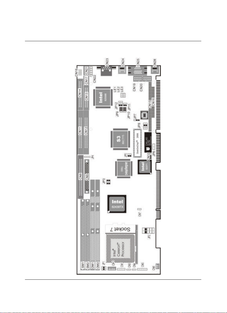
2.3 HS-5060’s Layout
11
Page 14

2.4 Quick Listing of Jumpers
JP1 ( Y 3-4 ) — CPU Clock-in Select
JP2 ( R 7-8 ) — CPU Vcore Voltage
JP3 ( Y 1-2, 5-6 ) — CPU Clock Based Select
JP4 ( B 2-3 ) — Manufacturer Default Setting
JP5 ( B 1-2 ) — DiskOnChip™ Address
JP6 ( Open ) — RTC Clear
JP7 ( B 1-2 ) — WATCHDOG Activ e Select
JP8 ( B 5-6 ) — Time of WATCHDOG
JP9 ( B 3-5, 4-6 ) — RS232 or RS232/422/485 Select
JP10 ( B 3-5, 4-6 ) — RS232 or RS232/422/485 Select
JP11 ( B 1-2 ) — RS232/422/485 Enable Control
JP12 ( B 1-2 ) — RS232/422/485 Data Control
??B means blue jumper-cap, R means read jumper-cap, Y means yellow jumper-cap.
??JP1 ( Y 3-4 ) means to use a yellow jumper-cap short between pin-3 and pin-4 of
JP1.
12
Page 15

2.5 Quick Listing of Connectors
CN1: SPEAKER
CN2: JST-5P KEYBOARD CONNECTOR
CN3: RESET IN CONNECTOR
CN4: IDE -DRIVE LED
CN5: KEYLOCK
CN6: FAN DC-POWER OUTPUT CONNECTOR
CN7: ATX POWER SUPPLY SUSPEND CONTROL
CN8: INTERNAL 50-PIN HEADER SCSI-III CONNECTOR
CN9: INTERNAL 68-PIN FEMALE D-SUB SCSI-III CONNECTOR
CN10: ATX POWER SWITCH CONTROL
CN11: 1st HDD(IDE) CONNECTOR
CN12: 2nd HDD(IDE) CONNECTOR
CN13: PARALLEL PORT
CN14: FDD CONNECTOR
CN15: PC/104 BUS 64-PIN HEADER CONNECOTR
CN16: PC/104 BUS 40-PIN HEADER CONNECOTR
CN17: RS -232/422/485 COM2 (HEADER 5x2)
CN18: USB0 & USB1
CN19: RS -232 COM2 (HEADER 5x2)
CN20: INTERNAL 10-PIN HEADER VGA CONNECTOR
CN21: RS -232 COM1 (HEADER 5x2)
CN22: IR CONNECTOR
CN23: RJ-45 LAN NETWORK CONNECTOR
CN25: MINI-DIN 6-PIN PS/2 MOUSE CONNECTOR
CN26: EXTERNAL DB -15 VGA CONNECTOR
CN28: MINI-DIN 6-PIN PS/2 KEYBOARD CONNECTOR
LD1: POWER LED INDICATO R
LE1, LE2, LE3: LAN NETWORK LED INDICATORs
13
Page 16

U17: SOCKET OF DiskOnChip™ MODULE
14
Page 17
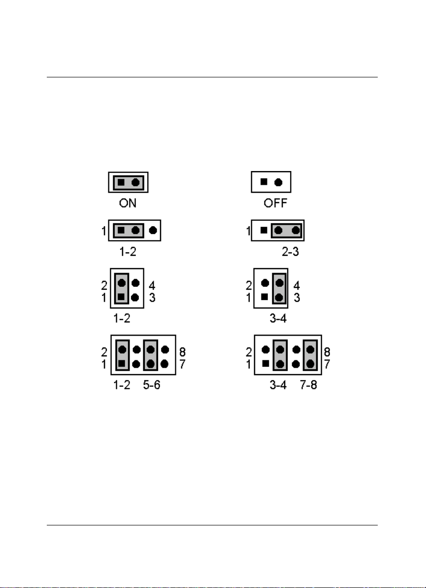
2.6 Jumper Setting Description
A jumper pin-set is ON as a shorted circuit with a plastic cap inserted over
two pins. A jumper pin-set is OFF as a open circuit with a plastic cap
inserted over one or no pin(s) between pins. The below figure 2.2 shows the
examples of different jumper pin-set setting as ON or OFF in this manual.
Figure 2.2
All jumper pin-set already has its default setting with the plastic cap
inserted as ON, or without the plastic cap inserted as OFF. The default
setting may reference in this manual with a " * " symbol in front of the
selected item.
15
Page 18
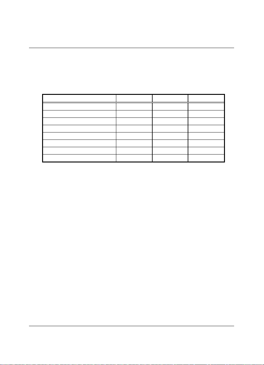
2.7 Setting the CPU of HS-5060
The HS -5060 provides all possibility in jumper setting for wide using all
types of CPU with JP1 setting as following:
?? CPU Clock Setting :
CPU Clock Ratio 1-2 3-4 5-6
2.0X ON OFF OFF
2.5X ON ON OFF
3.0X OFF ON OFF
3.5X OFF OFF OFF
4.0X ON OFF ON
4.5X ON ON ON
5.0X OFF ON ON
5.5X OFF OFF ON
16
Page 19
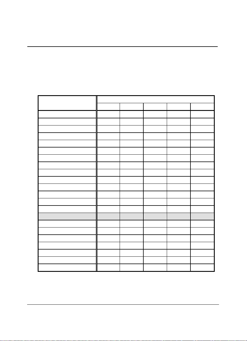
?? CPU Vcore Voltage Selection
Correspond to different type CPU, it is request to set JP2 for match the
CPU's Vcore operating voltage. Here shows at below of the proper jumper
settings for their respective Vcore at range 2.0V to 3.5V.
JP2 CPU Vcore
Voltage
9-10 7-8 5-6 3-4 1-2
1.80V ON ON OFF ON OFF
1.85V ON ON OFF ON ON
1.90V ON ON ON OFF OFF
1.95V ON ON ON OFF ON
2.00V ON ON ON ON OFF
2.05V ON ON ON ON ON
2.00V OFF OFF OFF OFF OFF
2.10V OFF OFF OFF OFF ON
2.20V OFF OFF OFF ON OFF
2.30V OFF OFF OFF ON ON
2.40V OFF OFF ON OFF OFF
2.50V OFF OFF ON OFF ON
2.60V OFF OFF ON ON OFF
2.70V OFF OFF ON ON ON
* 2.80V OFF ON OFF OFF OFF
2.90V OFF ON OFF OFF ON
3.00V OFF ON OFF ON OFF
3.10V OFF ON OFF ON ON
3.20V OFF ON ON OFF OFF
3.30V OFF ON ON OFF ON
3.40V OFF ON ON ON OFF
3.50V OFF ON ON ON ON
17
Page 20
JP3 used to setting the CPU clock based rate. The CPU clock based
setting will preset the system operating clocking base rate.
?? CPU Clock based select
CPU Clock based JP3
50 MHz 1-2, 3-4, 5-6
55 MHz 1-2, 3-4
60 MHz 3-4, 5-6
61.6 MHz 1-2
* 66.6 MHz 1-2, 5-6
68.4 MHz All OPEN
75 MHz 3-4
*) : default setting
2.8 System Memory DRAM
The HS -5060 provides a wide range on-board DRAM memory by two
pieces SIMM sockets ( SM1 & SM2 ) to accept 1 MB, 2MB, 4MB, 8MB,
16MB, 32MB or 64MB and two pieces DIMM sockets ( DM1 & DM2 ). The
SIMMs (Single In-Line Memory Modules) RAM request the access time
should be 70 n-second or faster. The total capacity of the on board
memory by SIMM are between 2MB to 128MB. The maximum capacity of
the on board memory by DIMM is 256MB.
See the figure on section 2.3 for get the identifying the banks. Please take
notes that the memory access capability should meet the specification
requested.
18
Page 21
2.9 Watch -Dog Timer
There are three activity cycles of Watch -Dog Timer as Enable, Refresh and
Disable. The Enable cycle should proceed by READ PORT 443H. The
Disable cycle should proceed by READ PORT 043H. A continue Enable
cycle after a first Enable cycle means Refresh.
Once if the Enable cycle activity, a Refresh cycle is request before the
time-out period for restart counting the WDT Timer's period. Otherwise, it
will assume that the program operation is abnormal when the time
counting over the period preset of WDT Timer. A System Reset signal to
start again or a NMI cycle to the CPU comes if over.
The JP7 is using for select the active function of watch -dog timer in disable
the watch -dog timer, or presetting the watch -dog timer activity at the reset
trigger, or presetting the watch-dog timer activity at the NMI trigger.
?? JP7 : Watch-Dog Active Type Setting
JP7 DESCRIPTION
*1-2 System Reset
2-3 Active NMI
OFF disable Watch-dog timer
?? JP8 : WDT Time - Out Period
PERIOD
*1 sec OFF OFF ON OFF
2 sec OFF OFF ON ON
10 sec OFF ON OFF OFF
20 sec
110 sec
220 sec
The Watch-dog timer is disabled after the system Power-On. The
watch-dog timer can be enabled by a Enable cycle with reading the control
port (443H), a Refresh cycle with reading the control port (443H) and a
Disable cycle by reading the Watch -dog timer disable control port (043H).
After a Enable cycle of WDT, user must constantly proceed a Refresh
1-2 3-4 5-6 7-8
OFF ON OFF ON
ON OFF OFF OFF
ON OFF OFF ON
19
Page 22

cycle to WDT before its period setting comes ending of every 1, 2, 10, 20,
110 or 120 seconds.
20
Page 23
If the Refresh cycle does not active before WDT period cycle, the on board
WDT architecture will issue a Reset or NMI cycle to the system. User
should pre-scale setting the JP8 for assign the WDT timeout cycle.
The Watch-Dog Timer is controlled by two I/O ports.
443H I/O Read The Enable cycle.
443H I/O Read The Refresh cycle.
043H I/O Read The Disable cycle.
The following sample programs showing how to Enable, Disable and
Refresh the Watch-dog timer:
WDT_EN_RF EQU 0443H
WDT_DIS EQU 0043H
WT_Enable PUSH AX ; keep AX DX
PUSH DX
MOV DX,WDT_EN_RF ; enable the watch-dog timer
IN AL,DX
POP DX ; get back AX, DX
POP AX
RET
WT_Rresh PUSH AX ; keep AX, DX
PUSH DX
MOV DX,WDT_ET_RF ; refresh the watch-dog timer
IN AL,DX
POP DX ; get back AX, DX
POP AX
RET
WT_DISABLE PUSH AX
PUSH DX
MOV DX,WDT_DIS ; disable the watch-dog timer
IN AL,DX
POP DX ; get back AX, DX
POP AX
RET
21
Page 24
2.10 PCI VGA Controller
The HS-5060 has built-in a S3® VGA Controller. If you want to use the
external VGA Card, th e BIOS can disable the on board VGA controller
and use the external one.
Video Modes
S3® 86C775 Chipset with 2 MB memory, support resolutions up to
1280 x 1024 256 colors, reserved internal 10 pin VGA connector.
To get more VGA drivers information, please refer to the S3 Internet
web site : WWW.S3.COM
2.11 DiskOnChip? Address Setting
The HS -5060 provides a U17 socket for install the DiskOnChip? module.
A JP5 may select the starting memory address of the DiskOnChip?
(D.O.C.) for avoid the mapping area with a ny other memory devices. If you
have another extra memory devices in the system with the same memory,
neither the HS -5060 nor the extra memory devices will function normally.
Please setting both at different memory address mapping.
?? JP5 : DiskOnChip? Addre ss
PIN NO. Address
*1-2 D000
3-4 D800
*) : default setting
The D.O.C. function allows the system in using without FDD nor HDD. The
D.O.C. may formatting as driver C: or driver A:. User may also easily uses
the DOS's commands such as FORMAT, SYS, COPY, XCOPY,
DISCOPY and DISKCOMP etc. This is means that the D.O.C. may uses
as driver-A if the system without FDD-A for ambient application. Please
contact with your supplier for different size D.O.C. module.
22
Page 25
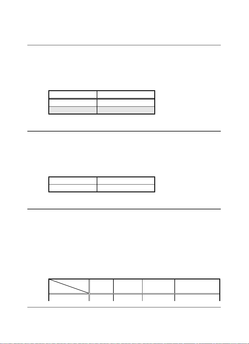
2.12 RTC Clear
The HS-5060 provides a JP6 for clear the RTC CMOS data. User may clear
the data by short ( ON ) the pins. Please keep OFF ( open ) when normal
operating.
?? JP6 : RTC CMOS Clear
JP6 Status
ON Clear Data
*OFF Normal Operating
*) : default setting
2.13 Manufacturer Default Setting
The HS -5060 has some engineering setting which does not allowed any
change by user. The information here in is for notice only, no technical
information provides in this section.
?? Manufacturer Default Setting
Jumper Default Setting
JP4 2-3 ON
*) : default setting
2.14 COM -2 Select and Control
This section descriptor how to select and control the COM-2 as an RS-232
or RS -232/422/485. Please reference to the following table for select and
control the port.
User may uses COM-2 as RS-232 port at CN19, and uses COM-2 as
RS-232/422/485 port at CN17. For more information, please reference to
section 3.4 in this manual.
?? COM-2 Port Select and Control
Jumper
JP9 JP10 JP11 JP12
Mode
RS-232 3-5, 4-6 3-5, 4-6 1-2 1-2
23
Page 26

RS-232/422/485 1-3, 2-4 1-3, 2-4 1-2 or 3-4 1-2 or 3-4 or 5-6
*) : default setting
24
Page 27
Chapter-3
Connection
This chapter gives all necessary information of the peripheral's
connections, switches and indicators.
3.1 The Floppy Disk Drive Connector
A standard 34-pin header daisy-chain driver connector provides as CN14
with following pin assignment. Total two FDD drivers may connect.
?? CN14 : FDD CONNECTOR
PIN NO. DESCRIPTION PIN NO.
1 GROUND 2 REDUCE WRITE
3 GROUND 4 N/C
5 GROUND 6 N/C
7 GROUND 8 INDEX#
9 GROUND 10 MOTOR ENABLE A#
11 GROUND 12 DRIVE SELECT B#
13 GROUND 14 DRIVE SELECT A#
15 GROUND 16 MOTOR ENABLE B#
17 GROUND 18 DIRECTION#
19 GROUND 20 STEP#
21 GROUND 22 WRITE DATA#
23 GROUND 24 WRITE DATA#
25 GROUND 26 TRACK 0#
27 GROUND 28 WRITE PROTECT#
29 GROUND 30 READ DATA#
31 GROUND 32 SIDE 1 SELECT
33 GROUND 34 DISK CHANGE#
DESCRIPTION
25
Page 28
3.2 PCI E-IDE Drive Connector
Two standard 40-pin header daisy-chain driver connectors provide as CN11
& CN12 with following pin assignment. Total four IDE (Integrated Device
Electronics) drivers may connect.
CN11(IDE 1) : Primary IDE Connector
CN12(IDE 2) : Secondary IDE Connector
?? CN11/CN12 : IDE Interface Connector
PIN NO. DESCRIPTION PIN NO.
1 RESET 2 GROUND
3 DATA 7 4 DATA 8
5 DATA 6 6 DATA 9
7 DATA 5 8 DA TA 10
9 DATA 4 10 DATA 11
11 DATA 3 12 DATA 12
13 DATA 2 14 DATA 13
15 DATA 1 16 DATA 14
17 DATA 0 18 DATA 15
19 GROUND 20 N/C
21 N/C 22 GROUND
23 IOW# 24 GROUND
25 IOR# 26 GROUND
27 N/C 28 BALE - DEFAULT
29 N/C 30 GROUND# -DEFAULT
31 INTERRUPT 32 IOCS16#-DEFAULT
33 SA1 34 N/C
35 SA0 36 SA2
37 HDC CS0 38 HDC CS1#
39 HDD ACTIVE 40 GROUND
DESCRIPTION
26
Page 29
3.3 Parallel Port Connector
A standard 26-pin flat cable driver connector provides as CN13 with
following pin assignment for connection to parallel printer.
?? CN13 : Parallel Port Connector
PIN NO.
1 STROBE 2 DATA 0
3 DATA 1 4 DATA 2
5 DATA 3 6 DATA 4
7 DATA 5 8 DATA 6
9 DATA 7 10 ACKNOWLEDGE
11 BUSY 12 PAPER EMPTY
13 PRINTER SELECT 14 AUTO FORM FEED
15 ERROR# 16 INITIALIZE
17 PRINTER SELECT LN#
19 GROUND 20 GROUND
21 GROUND 22 GROUND
23 GROUND 24 GROUND
25 GROUND 26 GROUND
DESCRIPTION PIN NO.
18 GROUND
DESCRIPTION
3.4 Serial Ports Connectors
The HS -5060 offers two high speeds NS16C550 compatible UARTs with
Read/Receive 16 byte FIFO serial ports provides one internal RS -232
COM-1 serial port, and one internal RS -232 or RS-232/422/485 port. All
ports provide by 10-pin header connector. The board provides CN21 as
COM-1 RS -232 port, CN19 as COM-2 RS-232 port, CN17 as COM-2
RS-232/422/485 port. The COM-2 port only select as CN19 or CN17.
Please reference to section 2.14 for COM-2 port selection.
27
Page 30
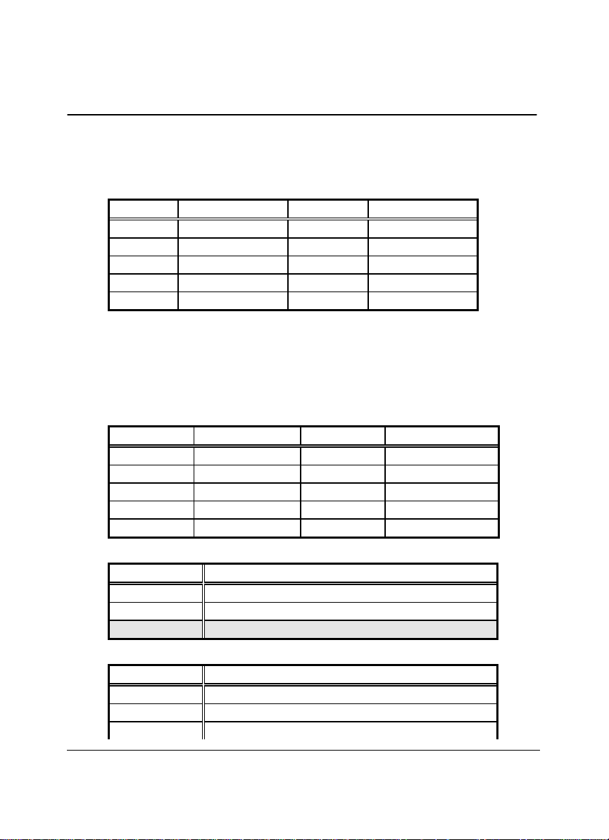
The following table shows out the pin assignment of CN21 and CN19 as
RS-232 communication ports of COM-1 and COM-2.
?? CN21, CN19 : Serial Port 10-pin Header (ACE1)
PIN NO. DESCRIPTION PIN NO. DESCRIPTION
1 DCD 2 DSR
3 RXD 4 RTX
5 TXD 6 CTX
7 DTR 8 RI
9 GND 10 NC
If the COM-2 select as an RS -232/422/485 port, the HS-5060 provides an
advanced setting at JP11 and JP12 for user to control the CN17 industrial
control output. Please reference to the following tables for CN17 detail
description.
?? CN17 : RS -232/422/485 Port 10-pin Header
PIN NO. DESCRIPTION PIN NO. DESCRIPTION
1 TX - 2 TX+
3 RX+ 4 RX5 GND 6 RTS7 RTS+ 8 CTS+
9 CTS- 10 NC
?? JP11 : Receiver Enable Control
JP11 CN17 DESCRIPTION
1-2 OFF Always Disable
3-4 ON Enable by writing the REG : 2 EFH BIT1=1
*1-2 ON Always Enable
?? JP12 : Transceiver Enable Control
JP12 CN17 DESCRIPTION
1-2 OFF Always Disable
3-4 ON Enable by ”-RTS” signal
5-6 ON Enable by writing the REG : 2 EFH BIT0=1
28
Page 31
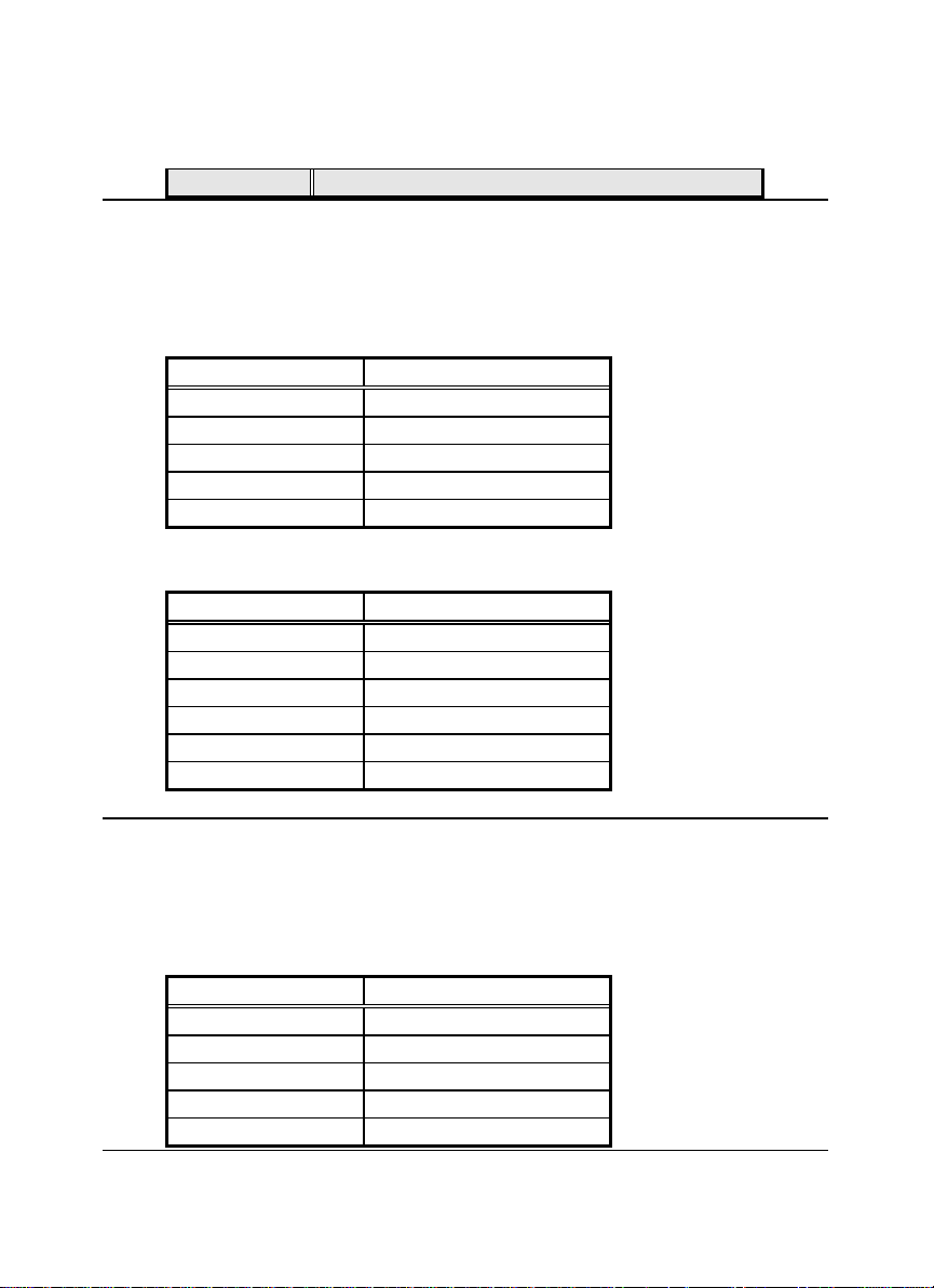
*1-2 ON Always Enable
3.5 Keyboard Connectors
The HS -5060 offers two possibilities for keyboard connections to external
PS/2 type keyboard at CN28, or an internal 5-pin header at CN2.
?? CN2 : 5-pin Header Keyboard Connector
PIN NO. DESCRIPTION
1 KEYBOARD CLOCK
2 KEYBOARD DATA
3 N/C
4 GROUND
5 +5V
?? CN28 : 6-pin Mini-DIN Keyboard Connector
PIN NO. DESCRIPTION
1 KEYBOARD DATA
2 N/C
3 GROUND
4 +5V
5 KEYBOARD CLOCK
6 N/C
3.6 Power's LED, Key -Lock and Reset Button
The following provides the pin information for Power's LED indicator,
Key-Lock and Reset Button connections from CN5, CN3 and CN4.
?? CN5 : POWER LED & KEYLOCK
PIN NO. DESCRIPTION
1 POWER LED ANODE
2 NC
3 GROUND
4 KEYLOCK
5 GROUND
29
Page 32

30
Page 33
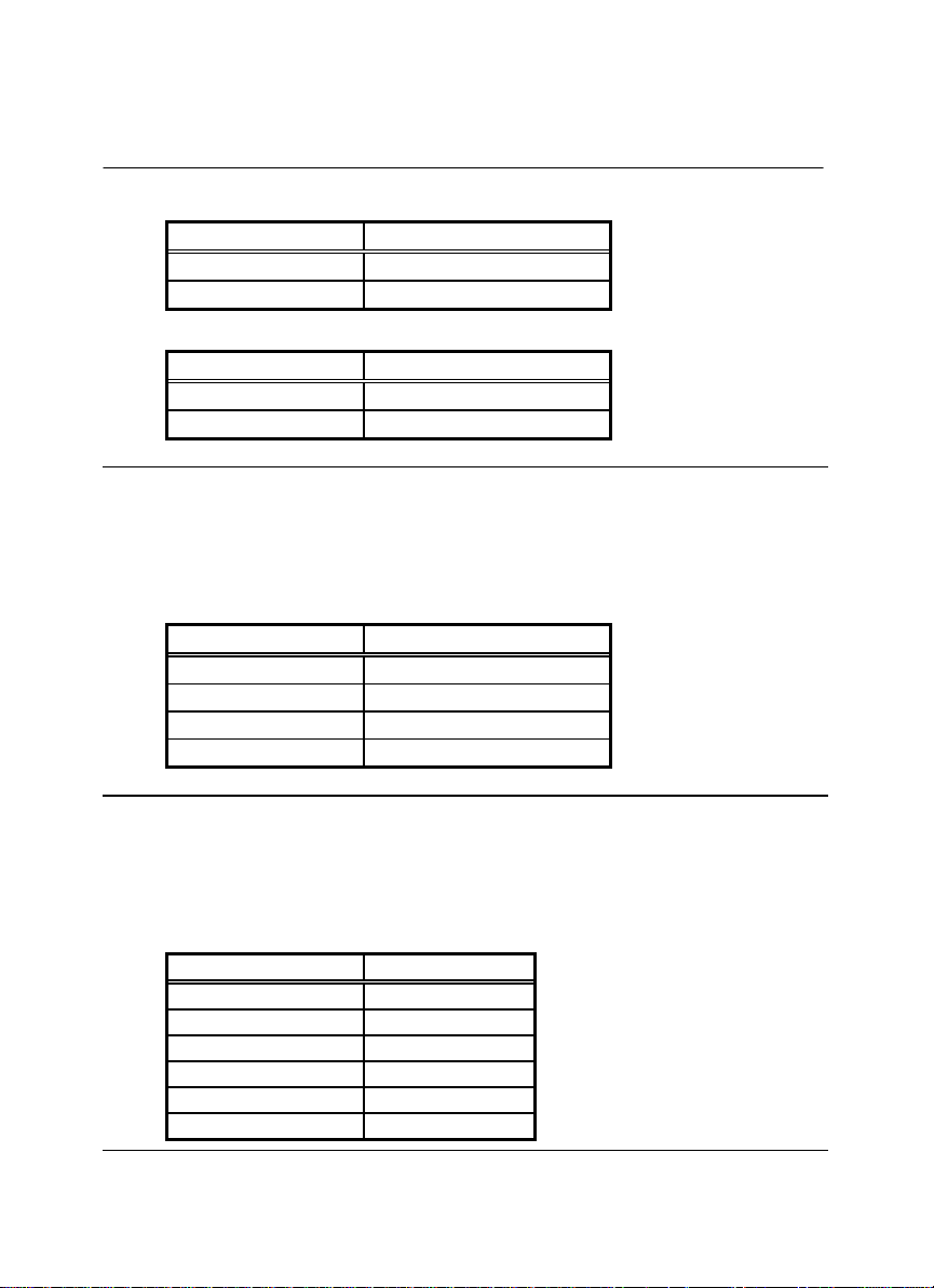
?? CN3 : RESET BUTTON
PIN NO. DESCRIPTION
1 GND
2 RESET
?? CN4 : IDE LED connector
PIN NO. DESCRIPTION
1 HDD ACTIVE#
2 +5V
3.7 External Speaker
The HS -5060 has an on-board buzzer. And it also provides the CN1 in
allows user to connecting to the external speaker.
?? CN1 : Speaker Connector
PIN NO. DESCRIPTION
1 SPEAKER SIGNAL
2 NC
3 GROUND
4 +5V
3.8 PS/2 Mouse 6-pin Mini-DIN Connector
The HS -5060 provides an external PS/2 mouse connector at CN25 with
following pin information.
?? CN25 : PS/2 Mouse Connector
PIN NO. DESCRIPTION
1 DATA
2 NC
3 GROUND
4 +5V
5 CLK
6 NC
31
Page 34
3.9 VGA Connectors
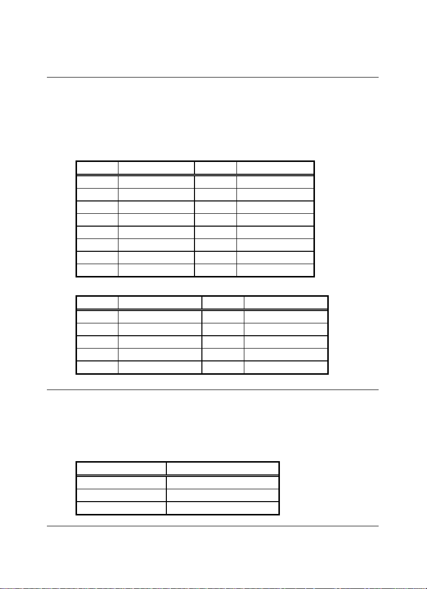
The HS-5060 provides two possible connectives of VGA connections. One
standard DB -15 external VGA connector CN26, and one internal 10-pin
header connector CN20 as following pin information.
?? CN26 : 15-pin DB-15 Female VGA connector
PIN NO. DESCRIPTION PIN NO. DESCRIPTION
1 RED 2 GREEN
3 BLUE 4 NC
5 GROUND 6 GROUND
7 GROUND 8 GROUND
9 NC 10 GROUND
11 NC 12 NC
13 HSYNC 14 VSYNC
15 NC
?? CN20 : 10-pin Header VGA connector
PIN NO. DESCRIPTION PIN NO. DESCRIPTION
1 RED 2 GROUND
3 GRE EN 4 GROUND
5 BLUE 6 GROUND
7 HSYNC 8 GROUND
9 VSYNC 10 GROUND
3.10 IR Connector
The HS -5060 provides a 5-pin internal IR communication connector as
following CN22 pin information.
?? CN22 : 5-PIN IR CONNECTOR
PIN NO. DESCRIPTION
1 Vcc
2 FIRRX
3 IRRX
32
Page 35

4 GROUND
5 IRTX
33
Page 36
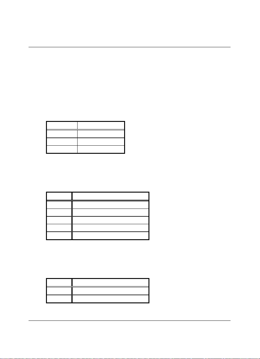
3.11 FAN -Power, Power-Suspend, ATX PowerSwitch Connectors
The HS-5060 provides more extra connector pin-set for user application in
power saving or system temperature control.
The CN6 FAN DC-Power output connector provides for connect to a
DC-FAN. The system will provide a DC +12V power to the cooling FAN.
?? CN6 : 3P FAN DC-Power Output Connector
PIN NO. DESCRIPTION
1 GROUND
2 DC +12V
3 GROUND
The CN7 ATX Power Supply Suspend Control connector provides for
connect to a ATX Power Supply.
?? CN7 : ATX Power Supply Suspend Control Connector
PIN NO.
1 NC
2 5VSB
3 NC
4 Control Single
5 GND
The CN10 SMI -Switch Input Control allows user to control the system and
force the system into a SMI mode ( The power suspend mode ).
DESCRIPTION
?? CN10 : 2P SMI-Switch Input Control Connector
PIN NO.
DESCRIPTION
1 3VSB
2 ATX Power Switch
34
Page 37

3.12 Power -ON LED Indicator
The HS -5060 provides a indicator LED LD1 to indicate the system power
status. A light ON means the power supply is under Power-ON operating.
3.13 Fast Ethernet Connector
The Fast Ethernet controller provides with 32-bit performance, PCI bus
master capability, and full compliance with IEEE 802.3 10/100Based-T
specifications.
For 10/100Base-T operation, please connect the network connection by
plugging one end of the cable into the 10-pin header of the CN23
Connector.
?? CN23 : Ethernet Connector ( RJ-45 9-pin )
PIN NO. DESCRIPTION
1 TX+
2 TX3 RX+
4 NC
5 NC
6 RX7 NC
8 NC
The on board three LED indicators ( LE1, LE2, LE3 ) will show out the
status of the LAN operating.
9 GROUND
3.14 SCSI-III Connector
The HS-5060 provides two internal SCSI -III connectors for all kinds of user
application and easy connection, one 50-pin header connector CN8 for
8-bit SCSI port and one 68-pin female D-Sub connector for 16-bit SCSI
port. Please reference to the following for detail pin assignment.
35
Page 38
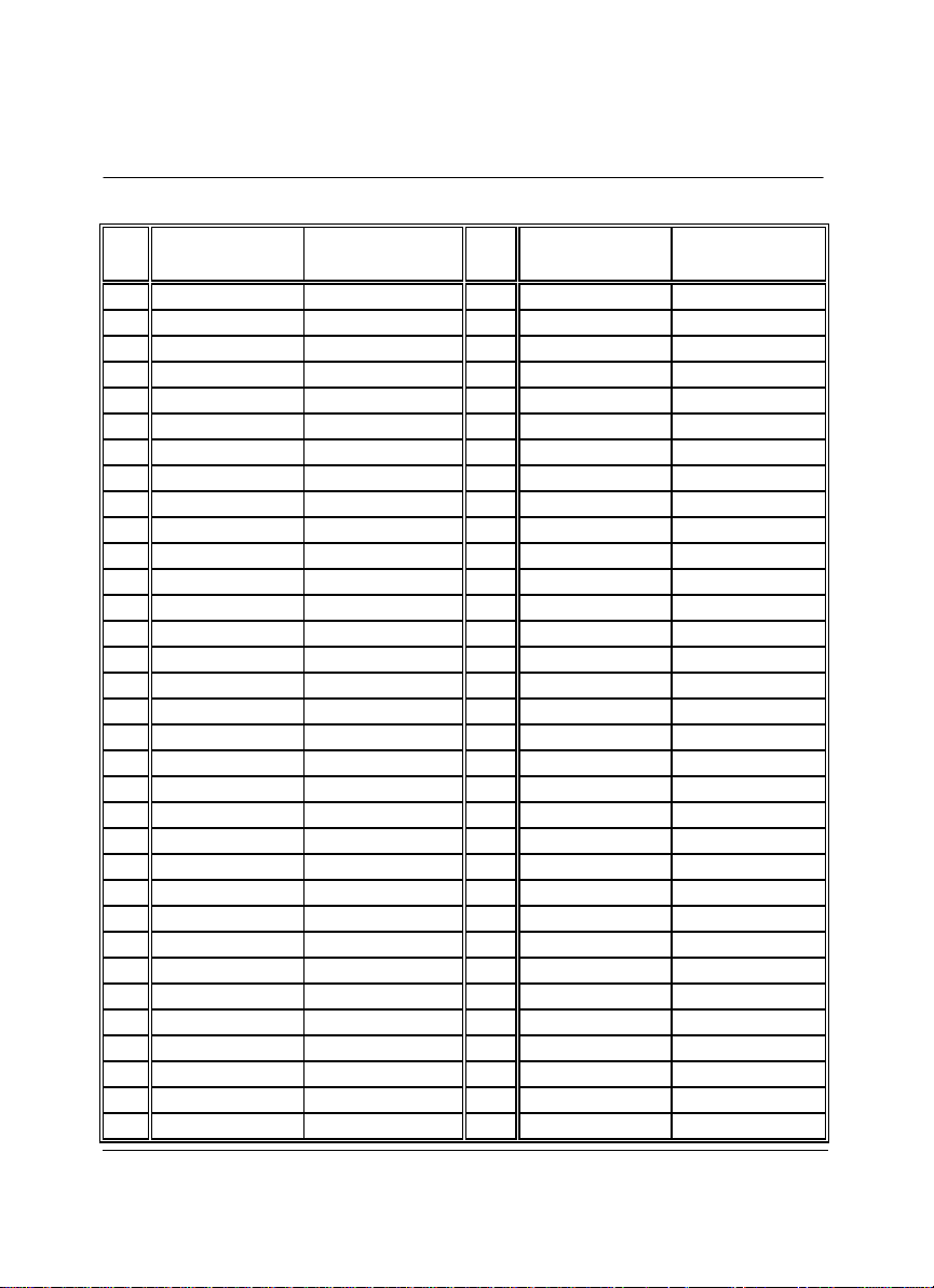
?? CN8 and CN9 Pin Assignment
Pin
1
2
3
4
5
6
7
8
9
10
11
12
13
14
15
16
17
18
19
20
21
22
23
24
25
26
27
28
29
30
31
32
33
CN8
Assignment
GROUND GROUND 35
SCD0 GROUND 36
GROUND GROUND 37
SCD1 GROUND 38
GROUND GROUND 39
SCD2 GROUND 40
GROUND GROUND 41
SCD3 GROUND 42
GROUND GROUND 43
SCD4 GROUND 44
GROUND GROUND 45
SCD5 GROUND 46
GROUND GROUND 47
SCD6 GROUND 48
GROUND GROUND 49
SCD7 GROUND 50
GROUND NC 51
SCDPL# NC 52
GROUND NC 53
GROUND GROUND 54
GROUND GROUND 55
GROUND GROUND 56
NC GROUND 57
NC GROUND 58
NC GROUND 59
VCC GROUND 60
NC GROUND 61
NC GROUND 62
GROUND GROUND 63
GROUND GROUND 64
GROUND GROUND 65
ATN# GROUND 66
GROUND GROUND 67
CN9
Assignment
Pin
CN8
Assignment
GROUND SCD12
BSY# SCD13
GROUND SCD14
ACK# SCD15
GROUND SCDPH#
RST# SCD0
GROUND SCD1
MSG# SCD2
GROUND SCD3
SEL# SCD4
GROUND SCD5
CD# SCD6
GROUND SCD7
REQ# SCDPL#
GROUND GROUND
IO# GROUND
VCC
VCC
NC
GROUND
ATN#
GROUND
BSY#
ACK#
RST#
MSG#
SEL#
CD#
REQ#
IO#
SCD8
SCD9
SCD10
CN9
Assignment
36
Page 39

34
GROUND GROUND 68
SCD11
37
Page 40
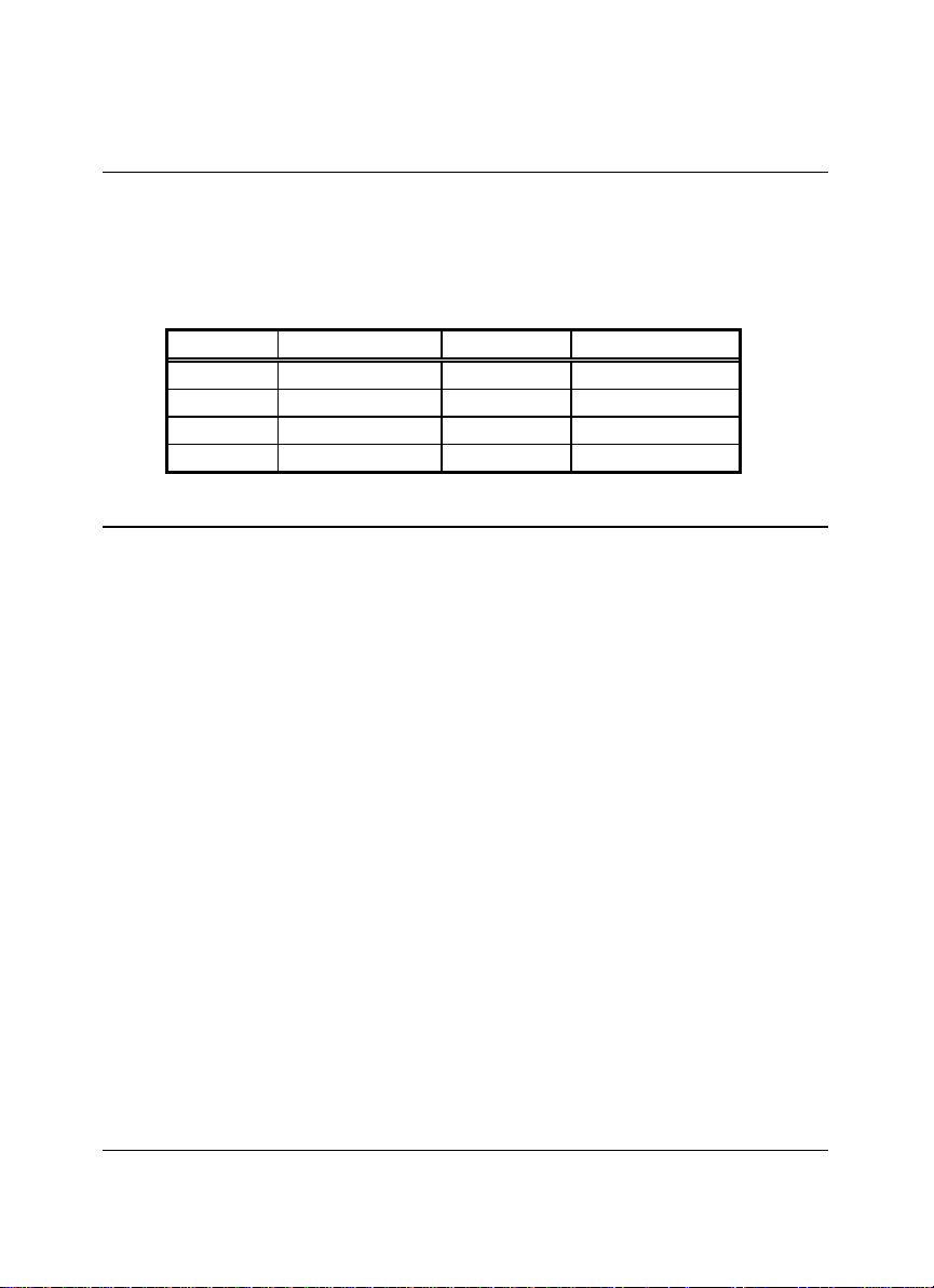
3.15 USB Ports Connector
The HS -5060 provides one internal 8-pin connector for USB0 & USB1
ports. Please refer to the following detail pin information.
?? CN18 : 10-pin Header USB0 & USB1 connector
PIN NO. CN18(USB0) PIN NO. CN18(USB1)
1 Vcc 2 Vcc
3 USBP0- 4 USBP15 USBP0+ 6 USBP1+
7 GROUND 8 GROUND
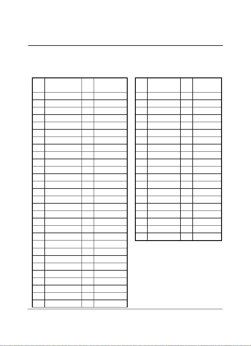
3.16 PC/104 Bus Connection
The HS -5060’s PC/104 expansion bus provides you in connect to all
kind of PC/104 modules. The PC/104 bus has been already become
the industrial embedded 16-bit PC standard bus. You can easily
install to over thousands type of PC/104 modules from hundreds of
venders in the world. The detailed pin assignment of the PC/104
expansion bus connectors CN15 and CN16 are specified as following
tables:
Note : The PC/104 connector allows to directly plug-in
Stack-thru PC/104 modules without the PC/104 mounting
kit.
38
Page 41
Pin
Pin
Pin
?? CN15&CN16 : PC/104 Expansion Bus
(CN15 = 64-pin female connector; CN16 = 40-pin female connector.)
Pin
No.
CN15
Row A
No.
CN15
Row B
No.
CN16
Row D
No.
1 IOCHECK* 33 0V 1 0V 21 0V
2 SD7 34 RESETDRV 2 MEMCS16* 22 SBHE*
3 SD6 35 +5V 3 IOSC16* 23 LA23
4 SD5 36 IRQ9 4 IRQ10 24 LA22
5 SD4 37 -5V 5 IRQ11 25 LA21
6 SD3 38 DRQ2 6 IRQ12 26 LA20
7 SD2 39 -12V 7 IRQ15 27 LA19
8 SD1 40 NOW* 8 IRQ14 28 LA18
9 SD0 41 +12V 9 DACK0* 29 LA17
10 IOCHRDY 42 (KEY) 10 DRQ0 30 MEMR*
11 AEN 43 SMEMW* 11 DACK5* 31 MEMW*
12 SA19 44 SMEMR* 12 DRQ5 32 SD8
13 SA18 45 IOW* 13 DACK6* 33 SD9
14 SA17 46 IOR* 14 DRQ6 34 SD10
15 SA16 47 DACK3* 15 DACK7* 35 SD11
16 SA15 48 DRQ3 16 DRQ7 36 SD12
17 SA14 49 DACK1* 17 +5V 37 SD13
18 SA13 50 DRQ1 18 MASTER* 38 SD14
19 SA12 51 REFRESH* 19 0V 39 SD15
20 SA11 52 SYSCLK 20 0V 40 (KEY)
21 SA10 53 IRQ7
22 SA9 54 IRQ6
23 SA8 55 IRQ5
24 SA7 56 IRQ4
25 SA6 57 IRQ3
26 SA5 58 DACK2*
27 SA4 59 TC
28 SA3 60 BALE
29 SA2 61 +5V
CN16
Row C
39
Page 42

30 SA1 62 OSC
31 SA0 63 0V
32 0V 64 0V
40
Page 43

Chapter-4
AWARD BIOS Setup
The HS-5060 uses the Award PCI/ISA BIOS for the system configuration.
The Award BIOS setup program is designed to provide the maximum
flexibility in configuring the system by offering various options which could
be selected for end-user requirements. This chapter is written to assist
you in the proper usage of these features.
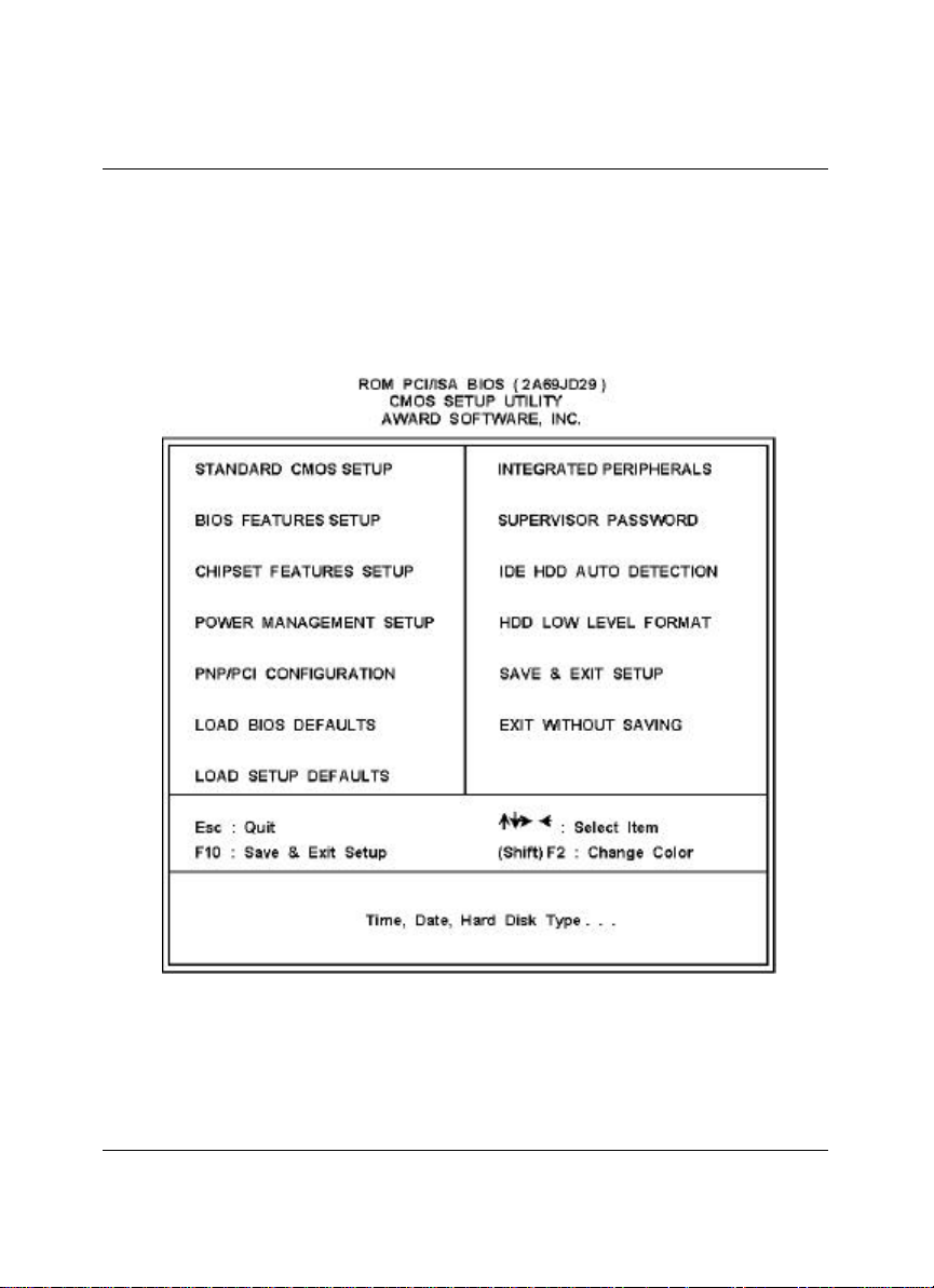
To access AWARD PCI/ISA BIOS Setup program, press <Del> key. The
Main Menu will be displayed at this time.
41
Page 44
4.1 Main Menu
Once you enter the Award BIOS CMOS Setup Utility, the Main Menu will
appear on the screen. The Main Menu allows you to select from several
setup functions and two exit choices. Use the arrow keys to select among
the items and press <Enter> to enter the sub-menu.
Note that a brief description of each highlighted selection appears at the
bottom of the screen.
42
Page 45
4.2 Standard CMOS Setup
0 0 0 0 0
0 0 0 0 0
0 0 0 0 0
0 0 0 0 0
The Standard Setup is used for the basic hardware system configuration.
The main function is for Data/Time and Floppy/Hard Disk Drive settings.
Please refer to the following screen for the setup. When the IDE hard disk
drive you are using is larger than 528MB, please set the HDD mode to LBA
mode. Please use the IDE Setup Utility in BIOS SETUP to install the HDD
correctly.
ROM PCI/ISA BIOS (2A59ID2A)
STANDARD CMOS SETUP
AWARD SOFTWARE, INC.
Data (mm:dd:yy) : Fri, Nov 15 1999
Time (hh:mm:ss) : 00:00:00
Primary Master ? Auto 0
Primary Slave ? Auto 0
Secondary Master : Auto 0
Secondary Slave : Auto 0
Drive A : 1.44M , 3.5in.
Drive B : None
Floppy 3 Mode Support : Disable Base Memory :
Video : EGA/VGA Extended Memory : 130048K
Halt On : All, But keyboard Total Memory : 131072K
ESC : Quit
F1 : Help
TYPE SIZE CYLS HEAD PRECOMP LANDZ SECTOR MODE
640K
Other Memory :
??? ? : Select Item
(Shift) F2: Change Color
PU/PD/ + / - : Modify
384K
AUTO
AUTO
AUTO
AUTO
43
Page 46
4.3 BIOS Features Setup
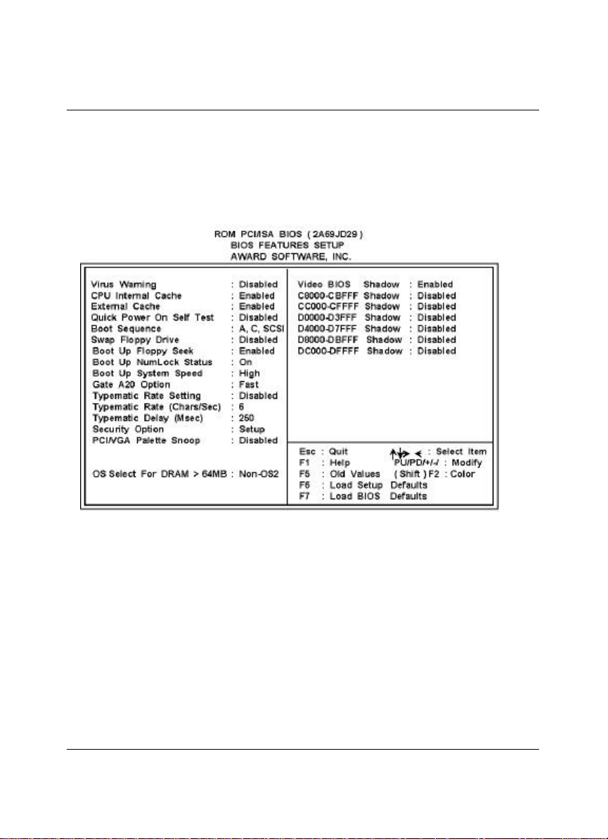
This section allows you to configure your system for the basic operation.
You have the opportunity to select the system’s default speed, boot -up
sequence, keyboard operation, shadowing and security.
44
Page 47

4.4 Chipset Features Setup
This section allows you to configure the system based on the specific
features of the installed chipset. This chipset manages bus speeds and
the access to the system memory resources, such as DRAM and the
external cache. It also coordinates the communications between the
conventional ISA and PCI buses. It must be stated that these items should
never be altered. The default settings have been chosen because they
provide the best operating conditions for your system. You might consider
and make any changes only if you discover that the data has been lost
while using your system.
ROM PCI/ISA BIOS (2A59ID2A)
CHIPSET FEATURES SETUP
AWARD SOFTWARE, INC.
Auto Configuration : Enabled DRAM Refresh Rate : 3
DRAM Speed Selection : 70 ns CPU Warming Temperature : 15.6 usd
DRAM Timing : 70 Current CPU Temperature : 65OC/149 OF
DRAM Read Burst (EDO/FP) : X333/X444
DRAM Write Burst Timing : X333
Fast EDO Lead off : Disabled
Refresh RAS# Assertion : 5 Clks
Fast RAS To RAS Delay : 3
DRAM Page Idle Timer : 2 Clks
DRAM Enhanced Paging : Enabled
Fast Ma to RAS# Delay : 2 Clks
Video BIOS Cacheable : Disabled
Video RAM Cacheable : Disabled
8 Bit I/O Recovery Time : 1
16 Bit I/O Recovery Time : 2
Memory Hole At 15M-16M : Disabled ESC : Quit ??? ? : Select Item
Passive Release : Enabled F1 : Help PU/PD/+/-: Modify
SDRAM (CAS Lat/RAS-to-CAS) : 3/3 F5 : Old Values (Shift) F2 : Color
SDRAM Sepculative Read : Disabled F6 : Load BIOS Defaults
PCI 2.1 Comliance : Disabled F7 : Load Setup Defaults
45
Page 48
4.5 Integrated Peripherals
The IDE hard drive controllers can support up to two separate hard drives.
These drives have a master/slave relationship, which are determined by
the cabling configuration used to attach them to the controller. Your
system supports two IDE cont rollers--a primary and a secondary--so you
can install up to four separate hard disks.
PIO means Programmed Input /Output. Rather than having the BIOS issue
a series of commands to affect the transfer to or from the disk drive, PIO
allows the BIOS to tell the controller what it wants and then let the
controller and the CPU perform the complete task by them. This is much
simpler and more efficient (also faster).
ROM PCI/ISA BIOS (2A59ID2A)
INTEGRATED PERIPHERALS
AWARD SOFTWARE, INC.
IDE HDD Block Mode : Enabled
IDE Primary Master PIO : Auto
IDE Primary Slave PIO : Auto
IDE Secondary Master PIO : Auto
IDE Secondary Slave PIO : Auto
IDE Primary Master UDMA : Auto Onboard Serial Port : 3F8/IRQ7
IDE Primary Slave UDMA : Auto Parallel Mode : SPP
IDE Secondary Master UDMA : Auto
IDE Secondary Slave UDMA : Auto
On Chip Primary PCI IDE : Enabled
On Chip Secondary PCI IDE : Enabled
Onboard PCI SCSI Chip : Enabled
USB Keyboard Support : Disabled
KBC input clock : 8M
Onboard FDC Controller : Enabled ESC : Quit ??? ? : Select Item
Onboard Serial Port 1 : 3F8/IRQ4 F1 : Help PU/PD/+/-: Modify
Onboard Serial Port 2 : 2F8/IRQ3 F5 : Old Values (Shift) F2 : Color
UART Mode Select : Normal F6 : Load BIOS Defaults
F7 : Load Setup Defaults
46
Page 49
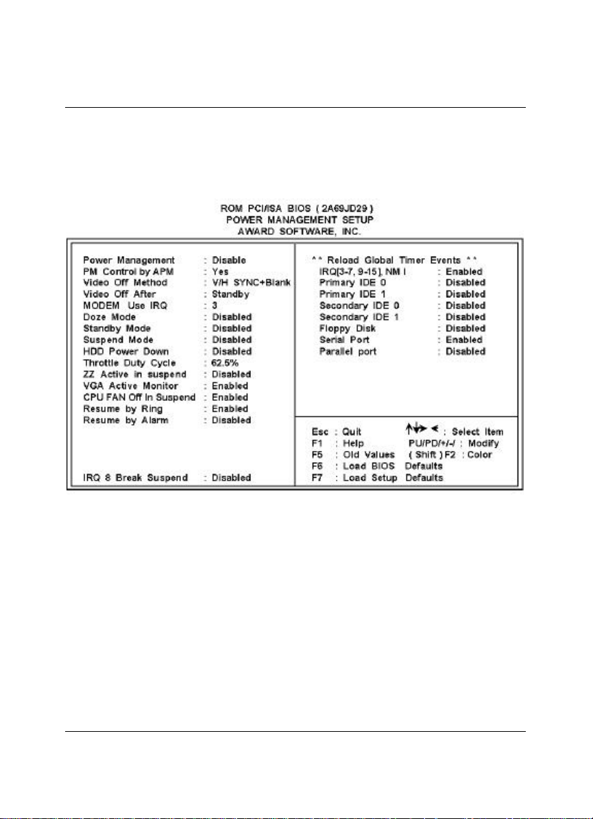
4.6 Power Management Setup
The Power Management Setup allows user to configure the system for
saving energy in a most effective way while operating in a manner
consistent with his own style of computer use.
47
Page 50

Chapter-5
A Brief Information of 10/100 based-T LAN
The HS -5060 provides an on board 32-bit PCI 10/100 based-T Intel™
82558A Ethernet LAN interface RJ-45 connection for easy using the
HS-5060 Half size all-in-one Pentium® VGA Interface with 100-Based
Network Industrial Single Board in connection to-with Novell NE2000
compatible LAN network system.
The HS -5060’s design that is basing on Intel™ 82558A chipset with
provides a RJ-45 100 base-T NE2000 compatible interfaces. For more
information, please contact with your supplier.
For completed information, please visit Intel Web and Internet Sites:
Support: http://support.intel.com
News: news://cs.intel.com
Network Products: http://www.intel.com/comm-net.sns
Corporate: http://www.intel.com
FTP Host: ftp.intel.com
FTP Directory:
/pub/support/enduser_reseller/etherexpress_lan_adapters
48
 Loading...