


HS-4706
HS-4706M
Intel® Pentium® M/ Celeron® M processor
ULV Intel
‧CompactFlash‧DDR‧PCI Slot‧
‧
‧ATA/33/66/100‧RS-232/422/485‧6 COM‧
‧
‧Industrial Embedded Engine Board‧
®
Celeron® M processor
Embedded Engine Board
CRT/LVDS Panel‧LAN‧Audio‧
USB2.0‧WDT‧H/W Monitor‧

Copyright Disclaimers
The accuracy of contents in this manual has passed thorough checking and review
before publishing. BOSER Technology Co., Ltd., the manufacturer and publisher, is
not liable for any infringements of patents or other rights resulting from its use. The
manufacturer will not be responsible for any direct, indirect, special,
incidental or consequential damages arising from the use of this product or
documentation, eve n i f ad vised of the possibility of such damage(s).
This manual is copyrighted and BOSER Technology Co., Ltd. reserv es all
documentation rights. Unauthorized reproduction, transmission, translation,
and storage of any form and means (i.e.,
recording) of this document, in whole or partly, is prohibited, unless granted
permission by BOSER Technology Co., Ltd.
BOSER Technology Co., Ltd.
contents of this document without due notice.
assumes no responsibility for any errors or omissions that may appear in this
manual, nor does it ma ke any com mitme nt to update the inform ation conta ined
herein.
T
r
a
d
e
m
a
r
k
s
T
r
a
d
e
m
T
r
a
d
e
m
BOSER is a registered trademark of BOSER Technology Co., Ltd.
ISB is a registered trademark of BOSER Technology Co., Ltd.
Intel is a registered trademark of Intel Corporation.
Award is a registered trademark of Award Software, Inc.
AMI is a registered trademark of AMI Software, Inc.
All other trademarks, products and or product names mentioned herein are
mentioned for identification purposes only, and may be trademarks and/or
registered trademarks of their respective companies or owners.
a
r
k
s
a
r
k
s
reserves the right to change or improve the
electronic, mechanical, photocopying,
BOSER Technology Co., Ltd.
© Copyright 2006 BOSER Technology Co., Ltd.
All Rights Reserved.
Edition 1.0 August 10, 2006

Table of Contents
Chapter 1 General Description..................................1
1.1
1.2
1.3
Major Features.............................................................2
Specifications ..............................................................3
Board Dimensions....................................................... 4
Chapter 2 Unpacking..................................................5
2.1
2.2
Opening the Delivery Package................................... 5
Inspection.....................................................................5
Chapter 3 Hardware Installation ..............................7
3.1
3.2
3.3
3.4
3.5
3.6
3.7
3.8
3.9
3.10
3.11
3.12
3.13
3.14
3.15
3.16
3.17
3.18
3.19
3.20
Before Installation....................................................... 7
Board Layout ...............................................................8
Jumper List .................................................................. 9
Connector List .................................. .... ....... .... .... .... ... .9
Configuring the CPU................................ ... .... .... .... ..10
System Memory.........................................................10
VGA Controller............................................................11
PCI E-IDE Drive Connector.......................................13
Floppy Disk Drive Connector................................... 15
Parallel Connector..................................................... 16
Serial Port Connectors..............................................17
Ethernet Connector...................................................18
USB Connector.......................................................... 19
CMOS Data Clear.......................................................19
Power and Fan Connectors......................................20
Keyboard/Mouse Connector .................................... 21
System Front Panel Connectors..............................21
Watchdog Timer.................................... .... ... .... .... .... ..22
Audio Connectors .....................................................23
CompactFlash™ Connector...................................... 23

Chapter 4 AMI BIOS Setup.....................................25
4.1
4.2
4.3
4.4
4.5
4.6
4.7
4.8
4.9
Starting Setup............................................................ 25
Main Menu.................................................................. 26
Advanced Settings.................................................... 27
Advanced PCI/PnP Settings.....................................34
Boot Settings ............................................................. 35
Security Settings.............................. ........ ... .... .... .... ..38
Advanced Chipset Settings......................................39
APM Configuration.................................................... 41
Exit Options ............................................................... 42
Chapter 5 Software Utilities.....................................43
5.1
5.2
5.3
5.4
5.5
IDE Driver Installation...............................................44
VGA Driver Installation..............................................48
5.2.1
5.2.2
5.2.3
5.3.1
5.3.2
5.3.3 WIN2K....................................................................................................................67
5.5.1
5.5.2
5.5.3
Win 98............... .........................................................................................48
Win NT.........................................................................................................51
Win 2000..................................................................................................53
LAN Driver Installation.............................................. 57
Win 98............... ..........................................................................................57
Win NT........................................................................................................60
Audio Driver Installation........................................... 70
USB2.0 Driver Installation.........................................72
Win 98............... ..........................................................................................72
Win 2000...................................................................................................76
Win XP........ ................................................................................................80

Safety Instructions
Integrated circuits on computer boards are sensitive t o static electricity.
To avoid damaging chips from electrostatic discharge, observe the
following precautions:
Do not remove boards or integrated circuits from their anti-static
packaging until you are ready to ins tall them.
Before handling a board or integrated circuit, touch an unpainted portion
of the system unit chassis for a few seconds. This helps to disch arge any
static electricity on your bo d y.
Wear a wrist-grounding strap, available from most electronic component
stores, when handling boards and components. Fasten the ALLIGATOR
clip of the strap to the end of the shielded wire lead from a grounded
object. Please wear and connect the strap before handling the HS-7250
to protect yourself from the discharge of any static electricity through the
strap.
Please use an anti-static pad when putting down any components or
parts or tools outside the computer. You may also use an anti-static bag
instead of the pad. Please inquire from your local supplier for additional
assistance in finding the necessary anti-static gadgets.
NOTE:
DO NOT TOUCH THE BOARD OR ANY OTHER SENSITIVE
COMPONENT WITHOUT ALL NECESSARY ANTI-S TATIC
PROTECTION.

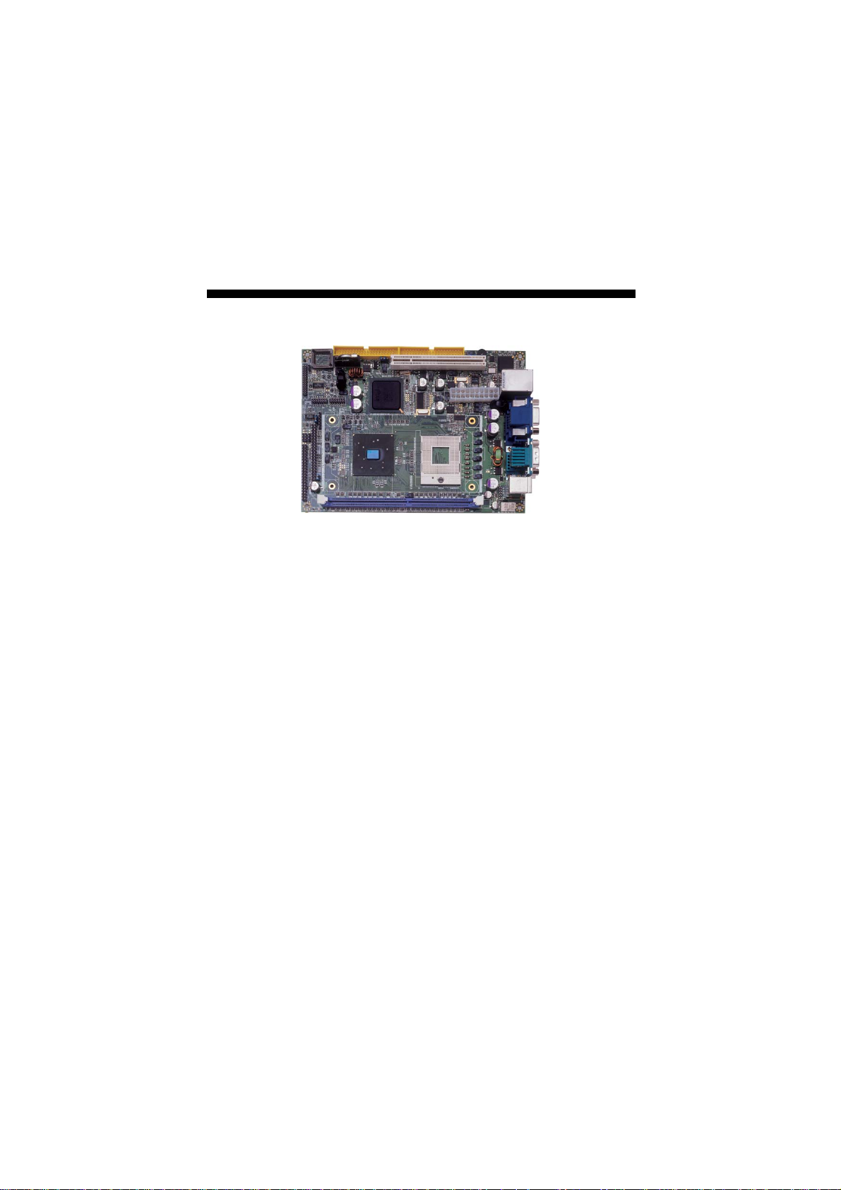
Chapter 1
General Description
The HS-4706/HS-4706M is an Intel® 852GME GMCH/ICH4
chipset-based and HS-4706/HS-4706M is and Intel
GMCH/ICH4 chipset-based board des igned embedded engine board.
HS-4706/HS-4706M provides Intel
1.3~2.8GHz, and HS-4706/HS-4706M provides ULV Intel
processor 600MHz. The combination of these features makes the
HS-4706/HS-4706M an ideal all-in-one industrial embedded engine
board. Additional features include an enhanced I/O with CF reader,
CRT/LVDS Panel, LAN, audio, 6 COM and USB2.0 port interface.
Its onboard ATA/33/66/100 connected to IDE drive interface
architecture allows the HS-4706 /HS-4706M to support data transfers
of 33, 66 or 100MB/sec. for each ID E drive connection. The display
controller is Intel
display supporting up to 1600 x 1200. It also provides 18-bit single
channel/36-bit dual channel LVDS Panel display interface.
System memory is also sufficient with the one DDR socke t that can
support up to 1GB. It also provides one IDE interface Type II
CompactFlash card adapter connector.
Additional onboard connectors includ e two internal and two external
USB2.0 ports providing faster data transmission, and one external
RJ-45 connector for use of one 10/100 Base-TX Ethernet interfaces.
®
82852GME (HS-4706)/852G M (HS- 47 06M ) for CRT
®
Pentium® M/Celeron® M processor
®
852GM
®
Celeron® M
1

1.1 Major Features
Front Side
Solder Side
The HS-4706/HS-4706M comes with the following features:
HS-4706 provides Intel® Pentium® M/Celeron® M processor 1.3~2.0GHz
HS-4706M provides ULV Intel Celeron M processor 600MHz/512K L2
cache
HS-4706 provides 400/533MHz FSB
One DDR socket with a max. capacity of 1GB
HS-4706 use Intel
HS-4706M use Intel
®
852GME GMCH/ICH4 system chipset
®
852GM GMCH/ICH4 system chipset
2

Winbond W83627HF super I/O chipset
HS-4706 use Intel
HS-4706M use Intel
LVDS Panel display interface
Intel
®
82551QM fast Ethernet controller
®
852GME GMCH/ICH4 system chipset
®
852GM GMCH/ICH4 system chipset
AC97 3D audio controller
Fast PCI ATA/33/66/100 IDE controller
CompactFlash card adapter, six COM, four USB2.0 ports
Hardware Monitor function
1.2 Specifications
CPU:
HS-4706 provides:
®
Intel
Pentium® M processor 760 2.0GHz
®
Intel
Pentium® M processor 745 1.8GHz
®
Intel
Celeron® M processor 370 1.5GHz
®
Intel
Celeron® M processor 320 1.3GHz
HS-4706M provides ULV Intel
cache
Front Side Bus: Supports 400/533MHz FSB (only HS-4706)
Memory: One DDR socket supporting up to 1GB
Chipset: Intel® 852GME GMCH/ICH4 (HS-4706), Intel® 852GM
GMCH/ICH4 (HS-4706M)
I/O Chipset: Winbond W83627HF
CompactFlash: One, Type II IDE interface adapter
PCI Slot:
VGA:
supporting CRT display up to 1600 x 1200
LVDS Panel: Supports 18-bit single channel/36-bit dual channel LVDS
interface
Ethernet: Intel
One standard PCI slot
®
Intel
82852GME (HS-4706) / Intel® 82852GM (HS-4706M)
®
82551QM 10/100 Based LAN
Audio: AC97 3D audio controller
IDE: Four IDE disk drives supporting ATA/33/66/100 with transfer rates
of up to 33/66/100MB/sec.
FDD: Supports one slim floppy disk drive
Parallel: One enhanced bi-directional parallel port supporting
SPP/ECP/EPP
Serial Port: 16C550 UART-compatible RS-232/485 x 1 and RS-232 x 5
serial ports with 16-byte FIFO
USB: Four USB2.0 ports, two internal and two external
®
Celeron® M processor 600MHz/512K L2
3

Keyboard: PS/2 6-pin Mini DIN
Mouse: PS/2 6-pin Mini DIN
BIOS: AMI PnP Flash BIOS
Watchdog Timer: Software programmable time-out intervals from
1~256 sec.
CMOS:
Temperature:
Hardware Monitor: Winbond W83627HF
Board Size: 20.3(L) x 14.6(W) x 3.3(H) cm
Battery backup
0~+60°C (operating)
1.3 Board Dimensions
4

Chapter 2
Unpacking
2.1 Opening the Delivery Package
The HS-4706/HS-4706M is packed in an anti-static bag. The board has
components that are easily damaged by static electricity. Do not
remove the anti-static wrapping until proper precautions have been
taken. Safety Instructions in front of this manual describe anti-static
precautions and procedures.
2.2 Inspection
After unpacking the board, plac e it on a raised surface and carefu lly
inspect the board for any damage that might have occurred during
shipment. Ground the board and exercise extreme care to prevent
damage to the board from static electricity.
Integrated circuits will sometimes come out of their sockets during
shipment. Make sure all integrated circuits, particularly the BIOS,
processor, memory modules , R OM -D i sk , and keyboard controller chip
are firmly seated. The HS-4706/HS-4706M delivery pac kage contains
the following items:
HS-4706/HS-4706M Board x 1
Utility CD Disk x 1
Cables Package x 1
Cooling Fan & Heat Sink x 1
Jumper Bag x 1
User’s Manual
5

Cables Package
NO. Description
1 Four COM flat cable x 1
2 ATA/100 IDE flat cable x 2
3 Two USB flat cable with bracket x 1
4 MIC/Audio flat cable with bracket x 1
5 Floppy cable x 1
6 Printer flat cable with bracket x 1
6

Chapter 3
Hardware Installation
This chapter provides the inform ation on how to install the hardware
using the HS-4706/HS-4706M. This chapte r also contains informa tion
related to jumper settings of switch, watchdog timer etc.
3.1 Before Installation
After confirming your package contents, you are now ready to install
your hardware. The following are important reminders and steps to
take before you begin with your installation process.
1. Make sure that all jumper settings match their default settings
and CMOS setup correctly. Refer to the sections on this chapter
for the default settings of each jumper. (Set JP1 1-2)
2. Go through the con nections of all external devices and make
sure that they are installed properly and configured correctly
within the CMOS setup. Refer to the sections on thi s chapter
for the detailed information on the connectors.
3. Keep the man u a l and diskette in good condition for future
reference and use.
7

3.2 Board Layout
8

3.3 Jumper List
Jumper
JP1 Clear CMOS: Normal Operation Short 1-2 19
JP2 Onboard LAN Function Enabled/Disabled Select: Enabled Short 1-2 18
JP3
JP4 Panel Voltage Select: +3.3V Short 2-3 11
JP5 CPU FSB Frequency Select: 400MHz FSB Short 3-4 10
COM 4 Use RS-232 or RS-422/485 Select: RS-232 Open 17
Default Setting Setting Page
3.4 Connector List
Connector Definition Page
CN1 COM 1/COM 2 Connector (DB9) 17
CN2 (1-15) 15-pin CRT Connector 11
CN2 (17-32)
CN3 (1-14) RJ-45 Connector 18
CN3 (23-30) Dual USB2.0 Ports 19
CN4 COM 3~COM 6 Connector (5x2 header) 17
CN6 RS-422/485 Connector (3x2 header) 17
CN7
CN8 (1-16) Control Panel Connector 21
CN8 (17-22) LAN LED Connector 18
CN8 (25-32) MIC In/Audio Out Connector 23
CN8 (33-40) Internal USB2.0 Ports 19
CN9
DM1 DDR Socket 10
FD1 Floppy Connector 15
FAN1 / FAN2 Fan Power In Connector 20
ID1 / ID2 Primary/Secondary IDE Connector 13
J1 Inverter Power In Connector 11
KR1 PS/2 6-pin Mini DIN KB and MS Connector 21
LP1 Parallel Port 16
PA1 / PA2 LVDS Panel Connector 11
PC1 Standard PCI Slot ----
PW1 20-pin ATX Power In Connector 20
External Audio Connector 23
2-pin ATX Power Switch 20
CompactFlash Connector 23
9

3.5 Configuring the CPU
The HS-4706 provides Intel® Pentium® M/Celeron® M processor
1.3~2.0GHz, and HS-4706M provides ULV Intel
®
Celeron® M
processor 600MHz/512K L2 cache. It offers the convenience in CPU
installation with its auto-detect feature. HS-4706 provides 400/533M Hz
FSB, if you want use 533MHz FSB, please setting JP5 as follow table.
JP5: CPU FSB Frequency Select (for HS-4706 only)
Options JP5(1-2) JP5(3-4)
400MHz (default) Open Short
533MHz
Open Open
1
3
2
4
Heat Sink Installation
Please smear the heat sink paste over CPU and 852GM GMCH
chipset uniformly. Then secure the heat sink as the picture above
3.6 System Memory
The HS-4706/HS-4706M provides one DDR so cket at location DM1.
The maximum capacity of the onboard memory is 1GB.
10

3.7 VGA Controller
The display controller is Intel® 82852GME (HS-4706)/82852GM
(HS-4706M) for CRT display supporting up to 1600 x 1200.
HS-4706/HS-4706M also provides 18-bit single channel/36-bit dual
channel LVDS display interface. The HS-4706/HS-4706M provides two
methods of connecting VGA device. CN2(1-15) offers a single
standard CRT connector (DB15), or PA1/PA2 offer 18-bit/36- bit LVDS
panel connectors.
CN2 (1-15): 15-pin CRT Connector (DB15)
PIN Description PIN Description
1 RED 2 GREEN
3 BLUE 4 N/C
5 GND 6 GND
7 GND 8 GND
9
N/C
11 N/C 12 SDA
13 HSYNC 14 VSYNC
15 SCL
J1: Inverter Power In Connector
PIN Description
1 +12V
2 +12V
3 +5V
4 BackLight Enabled
5 LCD Enabled
6 GND
JP4: Panel Voltage Select
Options Settings
+5V Short 1-2
+3.3V (default)
10
Short 2-3
GND
1 6
+3.3V
V
+5V
6
1
11
10
5
15
1
LCD
3
11

PA1: LVDS Panel Connector
PIN Description PIN Description
1 VCC3 2 VCC3
3 GND 4 GND
5 A0- 6 A0+
7 A1- 8 A1+
9 A2- 10 A2+
11 CLK1- 12 CLK1+
13 N/C 14 N/C
PA2: LVDS Panel Connector
PIN Description PIN Description
1
VCC3
2
3 GND 4 GND
5 A4- 6 A4+
7 A5- 8 A5+
9
A6-
10
11 CLK2- 12 CLK2+
13 N/C 14 N/C
VCC3
A6+
2
1
2
1
14
13
14
13
NOTE:
12
If using PA1 only, it just supports 18-bit single channel LVDS
Panel; If you want to use 36-bit dual channel LVDS Panel, please
using PA1 and PA2 combined.

3.8 PCI E-IDE Drive Connector
ID1 and ID2 are standard 40-pin daisy-chain driver connector that
serves the PCI E-IDE drive provisions onboard the
HS-4706/HS-4706M. A maximum of four ATA/33/66/100 IDE drives
can be connected to the HS-4706/HS-4706M via IDE1 and IDE2.
ID1: Primary IDE Connector
PIN Description PIN Description
1
RESET
2
3 PDATA 7 4 PDATA 8
5 PDATA 6 6 PDATA 9
7 PDATA 5 8 PDATA 10
9 PDATA 4 10 PDATA 11
11
PDATA 3
12
13 PDATA 2 14 PDATA 13
15 PDATA 1 16 PDATA 14
17 PDATA 0 18 PDATA 15
19 GND 20 N/C
21
PDREQ
22
23 PIOW# 24 GND
25 PIOR# 26 GND
27 PIORDY 28 PD1-
29 PDACK- 30 GND
31 Interrupt 32 N/C
33 PDA1- 34 PATA66
35 PDA0- 36 PDA2-
37 PCS1- 38 PCS3-
39 HDD Active 40 GND
GND
PDATA 12
GND
46810
2
1
3 5 7 9 17 19 21 23 25 27 29 31
12 14
11 13 15 35 37
202224 262830
16 36
18
32 34
38
40
39
33
13

ID2: Secondary IDE Connector
PIN Description PIN Description
1 RESET 2 GND
3 SDATA 7 4 SDATA 8
5 SDATA 6 6 SDATA 9
7 SDATA 5 8 SDATA 10
9
11 SDATA 3 12 SDATA 12
13 SDATA 2 14 SDATA 13
15 SDATA 1 16 SDATA 14
17 SDATA 0 18 SDATA 15
19
21 SDREQ 22 GND
23 SIOW# 24 GND
25 SIOR# 26 GND
27 SIORDY 28 SD1-
29 SDACK- 30 GND
31 Interrupt 32 N/C
33 SDA1- 34 SATA66
35 SDA0- 36 SDA2
37 SCS1- 38 SCS3-
39 HDD Active 40 GND
SDATA 4
GND
10
20
SDATA 11
N/C
14
46810
2
1
3 5 7 9 17 19 21 23 25 27 29 31
12 14
11 13 15 35 37
202224 262830
16 36
18
32 34
38
40
39
33

3.9 Floppy Disk Drive Connector
The HS-4706/HS-4706M uses a 26-pin connector, FD1, for one slim
floppy disk drive connection.
FD1: FDD Connector
PIN Description PIN Description
1
2 GND 15 Direction #
3 Read Data # 16 N/C
4 GND 17 Motor Enable 0
5 Write Protect # 18 N/C
6
7 Track0 # 20 N/C
8 N/C 21 Disk Change #
9 W gate # 22 VCC
10 GND 23 Driver 0
11
12 GND 25 Index #
13 Step # 26 VCC
Disk Select 1
N/C
Write Data #
14
19
24
N/C
N/C
VCC
126
15

3.10 Parallel Connector
LP1 is a standard 26-pin flat cable connector designed to
accommodate parallel port connection onboard the
HS-4706/HS-4706M.
LP1: Parallel Connector
PIN Description PIN Description
1 Strobe 14 Auto Form Feed
2 DATA 0 15 ERROR#
3
DATA 1
16
4 DATA 2 17 Printer Select LN#
5 DATA 3 18 GND
6 DATA 4 19 GND
7 DATA 5 20 GND
8
DATA 6
21
9 DATA 7 22 GND
10 Acknowledge 23 GND
11 Busy 24 GND
12 Paper Empty 25 GND
13 Printer Select 26 GND
Initialize
GND
16
Auto FormFeed
ERROR#
Initialize
Printer SelectLN#
GND
GND
GND
GND
GND
14
1
PDD0
PDD1
PDD2
PDD3
PDD4
PDD5
PDD6
Strobe
PDD7
GND
Acknowledge
GND
GND
GND
26
13
Busy
Paper Empty
Printer Select

3.11 Serial Port Connectors
The HS-4706/HS-4706M offers NS16C550 compatible UARTs
with Read/Receive 16-byte FIFO serial ports.
CN1: COM 1/COM 2 Connector (DB9)
PIN Description PIN Description
1 DCD1 10 DCD2
2 DSR1 11 DSR2
3 RXD1 12 RXD2
4 RTS1 13 RTS2
5 TXD1 14 TXD2
6 CTS1 15 CTS2
18
14
9
5
7 DTR1 16 DTR2
8 RI1 17 RI2
9 GND 18 GND
CN4: COM 3~COM 6 Con n ector (5x2 header)
PIN Description PIN Description
1 DCD3 2 DSR3
3 RXD3 4 RTS3
5 TXD3 6 CTS3
7 DTR3 8 RI3
9 GND 10 N/C
11 DCD4 12 DSR4
13 RXD4 14 RTS4
15 TXD4 16 CTS4
17 DTR4 18 RI4
19 GND 20 N/C
21 DCD5 22 DSR5
23 RXD5 24 RTS5
25
TXD5
26
27 DTR5 28 RI5
29 GND 30 N/C
31 DCD6 32 DSR6
33 RXD6 34 RTS6
35
TXD6
36
37 DTR6 38 RI6
39 GND 40 N/C
CTS5
CTS6
39 40
15
10
6
1
21
17

CN6: RS-422/485 Connector (3x2 header)
PIN Description PIN Description
1 TX- 2 TX+
3 RX+ 4 RX-
5 GND 6 VCC
2
1
6
5
JP3: COM 4 use RS-232 or RS-422/485 Select
Options Settings
RS-232 (default)
RS-485 by AUTO Short 5-7, 8-10
RS-485 by –RTS Short 7-9, 8-10
RS-422 Full Deplex Short 6-8
All Open
12
910
3.12 Ethernet Connector
The HS-4706/HS-4706M provides one 10/10 0 Base-TX LAN interfac e
connector. Please refer to the following for its pin information.
CN3(1-14): RJ-45 Connector
PIN Description PIN Description
1 RCT 2 TX+
3 TX- 4 RX+
5 RX- 6 N/C
7 N/C 8 N/C
9 N/C 10 RCT
11 Link LED 12 330Ω pull 3VSB
13 330Ω pull 3VSB 14 ACT LED
JP2: Onboard LAN Function Enabled/Disabled Select
Options Settings
Enabled (default) Short 1-2
13
Disabled Short 2-3
2
8
9
1
10
11
7
12
18

CN8(17-22): LAN LED Connector
PIN Description PIN Description
17 Link LED 18 330Ω pull 3VSB
19 ACT LED 20 330Ω pull 3VSB
21 Speed LED 22 330Ω pull 3VSB
40
139
2
3.13 USB Connector
The HS-4706/HS-4706M provides one 8-pin internal connector at
location CN8(33-40) and two 4-pin external connector, at locations
CN3(23-30), for four USB2.0 connections to the HS-4706/HS-4706M.
CN8(33-40): Internal USB2.0 Connector
PIN Description PIN Description
33 VCC 34 VCC
35 BD3- 36 BD4-
37
39 GND 40 GND
40
CN3(23-30): External USB2.0 Connector
BD3+
38
PIN Description PIN Description
23 VCC 24 VCC
25 BD1- 26 BD2-
27 BD1+ 28 BD2+
29 GND 30 GND
BD4+
139
2
3.14 CMOS Data Clear
The HS-4706/HS-4706 M has a Clear CMOS jumper on JP1.
JP1: Clear CMOS
Normal Operation (default) Short 1-2
IMPORTANT:
Options Settings
Clear CMOS S hort 2-3
Before you turn on the power of your system, please
set JP1 to short 1-2 for normal operation.
13
19

3.15 Power and Fan Connectors
HS-4706/HS-4706M provides one 20-pin ATX po wer in connector at
PW1, 2-pin ATX power switch at CN7.
PW1: 20-pin ATX Power In Connector
PIN Description PIN Description
1 +3.3V 11 +3.3V
2 +3.3V 12 -12V
3 GND 13 GND
4 +5V 14 PS_ON
5 GND 15 GND
6 +5V 16 GND
7 GND 17 GND
8 PWORK 18 -5V
9 +5Vsb 19 +5V
10 +12V 20 +5V
+3.3V
+3.3V
GND
+5V
GND
+5V
GND
PWORK
+5Vsb
+12V
111
-12V
+3.3V
CN7: 2-pin ATX Power Switch
PIN Description
1 Pull 220Ω to VCCSTBY
2 PS_ON
GND
GND
PS_ON
-5V
GND
GND
+5V
12
1020
+5V
FAN1/FAN2 onboard HS-4706/HS-4706M is 3-pin fan power
connector.
FAN1/FAN2: Fan Power Connector
PIN Description
1 GND
2 VCC12V
3 FAN Speed In
20
1
3

3.16 Keyboard/Mouse Connector
The HS-4706/HS-4706M offers one method for keyboard/mouse
connections. The connections a re done via KR1 for an external PS/2
type keyboard/mouse connection.
KR1: PS/2 6-pin Mini DIN Keyboard and Mouse Connector
PIN Description PIN Description
1 Keyboard Data 7 Mouse Data
2 N/C 8 N/C
3 GND 9 GND
4
+5V
10
5 Keyboard Clock 11 Mouse Clock
6 N/C 12 N/C
+5V
3412
5 6
91078
11
12
3.17 System Front Panel Connectors
The HS-4706/HS-4706M has one system front panel at location
CN8(1-16) that indicates the system front panel status.
CN8(1-16): System Front Panel Connector
PIN Description PIN Description
1 VCC 2 330Ω Pull VCC
3 GND 4 GND
5
GND
6
7 Speaker 8 N/C
9 GND 10 100Ω Pull +5Vsb
11 Reset Button 12 N/C
330Ω Pull VCC
13
14
15 HDD LED 16 N/C
40
GND
330Ω Pull +5Vsb
139
2
Connector CN8(1-16) Orientation
1
2
3
SPEAKER
RST_SW
HDD_LED
4
5
6
7
8
9
10
11
12
13
14
15
16
PWR LED
21

3.18 Watchdog Timer
Once the Enable cycle is active, a Refresh cycle is reques ted before
the time-out period. This restar ts counting of the WDT period. Wh en
the time counting goes over the period preset of WDT, it will assume
that the program operation is abnormal. A System Reset signal will
re-start when such error happens.
The following sample programs show how to Enable, Disable and
Refresh the Watchdog Timer:
;---------------------------------------------------------------------------------; Enter the WDT function mode, interruptible double-write
;--------------------------------------------------------------------------------- MOV DX, 2EH
MOV AL, 87H
OUT DX, AL
OUT DX, AL
MOV DX, 2EH
MOV AL, 07H
OUT DX, AL
MOV DX, 2FH
MOV AL, 08H
OUT DX, AL
MOV DX, 2EH
MOV AL, F5H
OUT DX, AL ; select CRF0
MOV DX, 2FH
MOV AL, 80H
OUT DX, AL
MOV DX, 2EH
MOV AL, F7H
OUT DX, AL
MOV DX, 2FH
MOV AL, 00H
OUT DX, AL
MOV DX, 2EH
MOV AL, F6H
OUT DX, AL
MOV DX, 2FH
MOV AL, 00H ; * 00H=Disabled
OUT DX, AL
;--------------------------------------------------------------------------------; Exit extended function mode
;------------- ------------------------------------------------------------------ MOV DX, 2EH
MOV AL, AAH
OUT DX, AL
User can also use AL, 00H’s defined time for reset purposes, e.g.00H
for Disable, 01H = 1sec, 02H = 2sec to FFH = 255sec.
22

3.19 Audio Connectors
The HS-4706/HS-4706M has an onboard AC97 3D audio interface.
The following tables list the pin assignme nts of the MIC In/Line Out
connectors.
CN2(17-32): Primary MIC In/Audio Out Connector
PIN Description PIN Description
17 GND 25 GND
18 LINE_IN R 26 GND
19
GND
27
20 GND 28 GND
21 GND 29 GND
22 LINE_IN L 30 GND
23 LINE_OUT R 31 GND
24 GND 32 MIC_IN 1
CN8(25-32): Secondary MIC In/Audio Out Connector
PIN Description PIN Description
25 Font LINE_OUT L 26 Font LINE _OUT R
27 GND 28 GND
29 MIC_IN 2 30 N/C
31 GND 32 GND
40
LINE_OUT L
139
2
3.20 CompactFlash™ Connector
The HS-4706/HS-4706M also offers an optional CompactFlash™
connector which is IDE interface located at the solder side of the board.
The designated CN9 connector, once soldered with an adapter, can
hold CompactFlash™ cards of various sizes. Please turn off the power
before inserting the CF card. Inserting a CompactFlash™ card into the
adapter is not a difficult task. The socket and card a re b oth ke yed a nd
there is only one direction for the card to be completely inserted. Refer
to the diagram below for the traditional way of inserting the card.
r
e
d
l
w
e
So
i
V
B
e
d
PC
i
S
M
T
sh
a
l
e
tF
d
i
/
S
n
n
r
o
a
mpac
a
p
p
a
o
a
e
J
J
C
R
u
n
i
A
F
e
e
d
C
u
a
q
i
M
r
b
a
F
E
C
23

This page is intentionally left blank.
24

Chapter 4
AMI BIOS Setup
The HS-4706/HS-4706M uses AMI BIOS for the sys tem con figur ation.
The AMI BIOS setup program is designed to provide the maximum
flexibility in configuring the system by offering various options that
could be selected for end-user requirements. This chapter is written to
assist you in the proper usage of these features.
4.1 Starting Setup
The AMI BIOS is immediately activated when you first power on the
computer. The BIOS reads the system information contained in the
CMOS and begins the process of checking out the system and
configuring it. When it finishes, the BIOS will seek an operating system
on one of the disks and then launch and turn control over to the
operating system.
While the BIOS is in control, the Setup program can be activated in one
of two ways:
1. By pressing <Del> immediately after switchin g th e system on, or
2. By pressing the <Del> key when the following message appears
briefly at the bottom of the screen during the POST (Power On Self
Test).
Press DEL to enter SETUP.
If the message disappears before you respond and you still wish to
enter Setup, restart the system to try again by turning it OFF then ON or
pressing the "RESET" button on the system case. You may also restart
by simultaneously pressing <Ctrl>, <Alt>, and <Delete> keys. If you do
not press the keys at the correct time and the system does not boot, an
error message will be displayed and you will again be asked to...
PRESS F1 TO CONTINUE, DEL TO ENTER SETUP
25

4.2 Main Menu
BIOS SETUP UTILTIY
Main Advanced PCIPnP Boot Security Chipset Power Exit
System Overview
AMIBIOS
Version :08.00.11
Build Date :03/09/06
ID :HS470600
Processor
Tyep :Intel(R) Celeron(R) M processor
Speed :1499MHz
Count :1
System Memory
Size :248MB
+ - Change Field
System Time [00:09:44] Tab Select Field
System Date [Tue 01/01/2002] F1 General Help
F10 Save and Exit
ESC Exit
v02.57 (C)Copyright 1985-2004, American Megatrends, Inc.
Use [ENTER], [TAB]
or [SHIFT-TAB] to
select a field.
Use [+] or [-] to
configure system
Time.
← →
Select Screen
↑ ↓
Select Item
26

4.3 Advanced Settings
BIOS SETUP UTILTIY
Main Advanced PCIPnP Boot Security Chipset Power Exit
Advanced Settings
WARNING: Setting wrong values in below
sections may cause system to malfunction.
X CPU Configuration
X IDE Configuration
Floppy Configuration
X
X SuperIO Configuration
Hardware Health Configuration
X
X ACPI Configuration
X MPS Configuration
X Smbios Configuration
X USB Configuration
↑ ↓ Select Item
+ - Change Field
Tab Select Field
F1 General Help
F10 Save and Exit
ESC Exit
v02.57 (C)Copyright 1985-2004, American Megatrends, Inc.
Configure CPU.
← →
Select Screen
27

BIOS SETUP UTILTIY
Main Advanced PCIPnP Boot Security Chipset Power Exit
Configure advanced CPU settings
Module Version –12.00
Manufacturer :Intel
Brand String :Intel(R) Celeron(R) M processor
Frequency :1.49GHz
FSB Speed :400MHz
Cache L1 :32 KB
Cache L2 :1024 KB
Execute Disable Bit [Enabled] ↑ ↓ Select Item
CPU TM function: [Enabled] + - Change Field
Tab Select Field
F1 General Help
Hyper Threading Technology [Enabled] F10 Save and Exit
ESC Exit
v02.57 (C)Copyright 1985-2004, American Megatrends, Inc.
BIOS SETUP UTILTIY
Main Advanced PCIPnP Boot Security Chipset Power Exit
IDE Configuration
OnBoard PCI IDE Controller [Both]
OnBoard PCI IDE Operate Mode [Legacy Mode]
X Primary IDE Maste r : [Not Detected]
Primary IDE Slave : [ATAPI CDROM]
X
X Secondary I DE Master : [Not Detected]
Secondary IDE Sla ve : [Not Detected ]
X
← → Select Screen
Hard Disk Write Protect [Disabled]
IDE Detect Time Out (Sec) [35] + - Change Field
ATA(PI) 80Pin Cable Detection [Host & Device] Tab Select Field
F1 General Help
F10 Save and Exit
ESC Exit
v02.57 (C)Copyright 1985-2004, American Megatrends, Inc.
When disabled, force
the XD feature flag to
always return 0.
← →
Select Screen
Disabled: disables
the integrated IDE
Controller.
PRIMARY: enables
only the Primary IDE
Controller.
SECONDARY: enables
only the Secondary
IDE Controller.
Both: enables both
IDE Controllers.
↑ ↓
Select Item
28

BIOS SETUP UTILTIY
Main Advanced PCIPnP Boot Security Chipset Power Exit
Floppy Configuration
Floppy A [1.44 MB 3.5”]
Floppy B [Disabled]
+ - Change Field
Tab Select Field
F1 General Help
F10 Save and Exit
ESC Exit
v02.57 (C)Copyright 1985-2004, American Megatrends, Inc.
Select the type of
floppy drive
connected to the
system.
← →
Select Screen
↑ ↓
Select Item
BIOS SETUP UTILTIY
Main Advanced PCIPnP Boot Security Chipset Power Exit
Configure Win627 Super IO Chipset
OnBoard Floppy Controller [Enabled]
Floppy Drive Swap [Disabled]
Serial Port1 Address [3F8/IRQ4]
Serial Port2 Address [2F8/IRQ3]
Serial Port2 Mode [Normal]
OnBoard CIR Port [Disabled]
Parallel Port Address [378]
Parallel Port Mode [ECP]
ECP Mode DMA Channel [DMA3]
Parallel Port IRQ [IRQ7]
OnBoard Game Port [Disabled] + - Change Field
OnBoard MIDI Port [Disabled] Tab Select Field
Serial Port3 Address [3E8] F1 General Help
Serial Port3 IRQ [10] F10 Save and Exit
Serial Port4 Address [2E8] ESC Exit
Serial Port4 IRQ [11]
Serial Port5 Address [2F0]
Serial Port5 IRQ [11]
Serial Port6 Address [2E0]
Serial Port6 IRQ [11]
v02.57 (C)Copyright 1985-2004, American Megatrends, Inc.
Allows BIOS to
Enable of Disable
Floppy Controller.
← →
Select Screen
↑ ↓
Select Item
29

BIOS SETUP UTILTIY
Main Advanced PCIPnP Boot Security Chipset Power Exit
Hardware Health Configuration
H/W Health Function [Enabled]
Chassis Intrusion [Disabled]
Hardware Health Event Monitoring
CPU Temperature :21°C/69°F
System Temperature :18°C/64°F
System Fan :5273RPM + - Change Field
Tab Select Field
VcoreA :1.258 V F1 General Help
+3.3Vin :3.419 V F10 Save and Exit
+5Vin :5.107 V ESC Exit
+12Vin :12.160 V
v02.57 (C)Copyright 1985-2004, American Megatrends, Inc.
BIOS SETUP UTILTIY
Main Advanced PCIPnP Boot Security Chipset Power Exit
ACPI Settings
ACPI Aware O/S [Yes]
General ACPI Configuration
X
X Advanced ACPI Configuration
X Chipset ACPI Configuration
← → Select Screen
+ - Change Field
Tab Select Field
F1 General Help
F10 Save and Exit
ESC Exit
v02.57 (C)Copyright 1985-2004, American Megatrends, Inc.
Enables Hardware
Health Monitori ng
Device.
← →
Select Screen
↑ ↓
Enable / Disable ACPI
support for Operating
System.
ENABLE: If OS
supports ACPI.
DISABLE: If OS does
not support ACPI.
↑ ↓
Select Item
Select Item
30

BIOS SETUP UTILTIY
Main Advanced PCIPnP Boot Security Chipset Power Exit
General ACPI Configuration
Suspend mode [Auto]
Repost Video on S3 Resume [No]
↑ ↓ Select Item
+ - Change Field
Tab Select Field
F1 General Help
F10 Save and Exit
ESC Exit
v02.57 (C)Copyright 1985-2004, American Megatrends, Inc.
Select the ACPI state
used for System
Suspend.
← →
Select Screen
BIOS SETUP UTILTIY
Main Advanced PCIPnP Boot Security Chipset Power Exit
Advanced ACPI Configuration
ACPI 2.0 Features [No]
ACPI APIC support [Enabled]
AMI OEMB table [Enabled]
Headless mode [Disabled]
← → Select Screen
+ - Change Field
Tab Select Field
F1 General Help
F10 Save and Exit
ESC Exit
v02.57 (C)Copyright 1985-2004, American Megatrends, Inc.
Enable RSDP pointers
to 64-bit Fixed
System Description
Tables.
↑ ↓
Select Item
BIOS SETUP UTILTIY
Main Advanced PCIPnP Boot Security Chipset Power Exit
APIC ACPI SCI IRQ [Disabled]
USB Device Wakeup From S3 [Disabled]
+ - Change Field
Tab Select Field
F1 General Help
F10 Save and Exit
ESC Exit
v02.57 (C)Copyright 1985-2004, American Megatrends, Inc.
← →
Select Screen
↑ ↓
Select Item
31

BIOS SETUP UTILTIY
Main Advanced PCIPnP Boot Security Chipset Power Exit
MPS Configuration
MPS Revision [1.4]
+ - Change Field
Tab Select Field
F1 General Help
F10 Save and Exit
ESC Exit
v02.57 (C)Copyright 1985-2004, American Megatrends, Inc.
BIOS SETUP UTILTIY
Main Advanced PCIPnP Boot Security Chipset Power Exit
Smbios Configuration
Smbios Smi Support [Enabled]
+ - Change Field
Tab Select Field
F1 General Help
F10 Save and Exit
ESC Exit
v02.57 (C)Copyright 1985-2004, American Megatrends, Inc.
Select MPS Revision.
← →
Select Screen
↑ ↓
SMBIOS SMI Wrapper
support for PnP Func
50h-54h
← →
↑ ↓
Select Item
Select Screen
Select Item
32

BIOS SETUP UTILTIY
Main Advanced PCIPnP Boot Security Chipset Power Exit
USB Configurat ion
Module Version –2.24.0-10.4
USB Devices Enable :
None
USB Function [4 USB Ports]
Legacy USB Support [Enabled]
USB 2.0 Controller [Enabled]
USB 2.0 Controller Mode [ H iSpeed]
BIOS EHCI Hand-Off [Enabled] ← → Select Screen
↑
+ - Change Field
Tab Select Field
F1 General Help
F10 Save and Exit
ESC Exit
v02.57 (C)Copyright 1985-2004, American Megatrends, Inc.
Enables USB host
controllers.
↓
Select Item
33

4.4 Advanced PCI/PnP Settings
BIOS SETUP UTILTIY
Main Advanced PCIPnP Boot Security Chipset Power Exit
Advanced PCI/PnP Settings
WARNING: Setting wrong values in below
sections may cause system to malfunction.
Clear NVRAM [No]
Plug & Play O/S [No]
PCI Latency Timer [64]
Allocate IRQ to PCI VGA [Yes]
Palette Snooping [Disabled]
PCI IDE BusMaster [Enabled]
OffBoard PCI/ISA IDE Card [Auto]
IRQ3 [Available]
IRQ4 [Available]
IRQ5 [Available] + - Change Field
IRQ7 [Available] Tab Select Field
IRQ9 [Available] F1 General Help
IRQ10 [Available] F10 Save and Exit
IRQ11 [Available] ESC Exit
IRQ14 [Available]
IRQ15 [Available]
DMA Channel 0 [Available]
DMA Channel 1 [Available]
DMA Channel 3 [Available]
DMA Channel 5 [Available]
DMA Channel 6 [Available]
DMA Channel 7 [Available]
Reserved Memory Size [Disa bled]
v02.57 (C)Copyright 1985-2004, American Megatrends, Inc.
Clear NVRAM during
System Boot.
← →
Select Screen
↑ ↓
Select Item
34

4.5 Boot Settings
BIOS SETUP UTILTIY
Main Advanced PCIPnP Boot Security Chipset Power Exit
Boot Settings
X Boot Settings Configuration
X Boot Device Priority
Removable Drives
X
X CD/DVD Drives
+ - Change Field
Tab Select Field
F1 General Help
F10 Save and Exit
ESC Exit
v02.57 (C)Copyright 1985-2004, American Megatrends, Inc.
BIOS SETUP UTILTIY
Main Advanced PCIPnP Boot Security Chipset Power Exit
Boot Settings Configuration
Quick Boot [Enabled]
Quiet Boot [Disabled]
AddOn ROM Display Mode [Force BIOS]
Bootup Num-Lock [On]
PS/2 Mouse Support [Auto]
Wait For ‘F1’ If Error [Enabled]
Hit ‘DEL’ Message Display [Enabled]
Interrupt 19 Capture [Disabled]
+ - Change Field
Tab Select Field
F1 General Help
F10 Save and Exit
ESC Exit
v02.57 (C)Copyright 1985-2004, American Megatrends, Inc.
Configure Settings
during System Boot.
← →
Select Screen
↑ ↓
Allows BIOS to skip
certain tests while
booting. This will
decrease the time
needed to boot the
system.
← →
↑ ↓
Select Item
Select Screen
Select Item
35

BIOS SETUP UTILTIY
Main Advanced PCIPnP Boot Security Chipset Power Exit
Boot Device Priority
1st Boot Device [1st FLOPPY DRIVE]
2nd Boot Device [CD/DVD:PS-ASUS CRW]
+ - Change Field
Tab Select Field
F1 General Help
F10 Save and Exit
ESC Exit
v02.57 (C)Copyright 1985-2004, American Megatrends, Inc.
BIOS SETUP UTILTIY
Main Advanced PCIPnP Boot Security Chipset Power Exit
Removable Drives
1st Drive [1st FLOPPY DRIVE]
+ - Change Field
Tab Select Field
F1 General Help
F10 Save and Exit
ESC Exit
v02.57 (C)Copyright 1985-2004, American Megatrends, Inc.
Specifies the boot
sequence from the
available devices.
A device enclosed in
parenthesis has been
disabled in the
corresponding type
menu.
← →
Select Screen
↑ ↓
Specifies the boot
sequence from the
available devices.
← →
↑ ↓
Select Item
Select Screen
Select Item
36

BIOS SETUP UTILTIY
Main Advanced PCIPnP Boot Security Chipset Power Exit
CD/DVD Drives
1st Device [CD/DVD:PS-ASUS CRW]
↑ ↓ Select Item
+ - Change Field
Tab Select Field
F1 General Help
F10 Save and Exit
ESC Exit
v02.57 (C)Copyright 1985-2004, American Megatrends, Inc.
Specifies the boot
sequence from the
available devices.
← →
Select Screen
37

4.6 Security Settings
BIOS SETUP UTILTIY
Main Advanced PCIPnP Boot Security Chipset Power Exit
Security Settings
Supervisor Password :Not Installed
User Password :Not Installed
Change Supervisor Password
Change User Password
Boot Sector Virus Protection [Disabled]
← → Select Screen
↑
+ - Change Field
Tab Select Field
F1 General Help
F10 Save and Exit
ESC Exit
v02.57 (C)Copyright 1985-2004, American Megatrends, Inc.
Install or Change the
password.
↓
Select Item
38

4.7 Advanced Chipset Settings
BIOS SETUP UTILTIY
Main Advanced PCIPnP Boot Security Chipset Power Exit
Advanced Chipset Settings
WARNING: Setting wrong values in below
sections may cause system to malfunction.
X NorthBridge Configuration
X SouthBridge Configuration
← → Select Screen
+ - Change Field
Tab Select Field
F1 General Help
F10 Save and Exit
ESC Exit
v02.57 (C)Copyright 1985-2004, American Megatrends, Inc.
BIOS SETUP UTILTIY
Main Advanced PCIPnP Boot Security Chipset Power Exit
DRAM Frequency [Auto]
Configure DRAM Timing by SPD [Enabled]
Memory Hole [Disabled]
Init. Graphic Adapter Priority [Internal VGA]
Internal Graphics Mode Select [Enabled, 8MB]
Graphics Aperture Size [ 64MB] ← → Select Screen
Boot Display Device [CRT+LFP] + - Change Field
Flat Panel Type [800x600LVDS] Tab Select Field
TV Standard [Auto] F1 General Help
F10 Save and Exit
ESC Exit
v02.57 (C)Copyright 1985-2004, American Megatrends, Inc.
Options for NB
↑ ↓
200Mhz
266Mhz
333Mhz
Auto
↑ ↓
Select Item
Options
Select Item
39

BIOS SETUP UTILTIY
Main Advanced PCIPnP Boot Security Chipset Power Exit
OnBoard AC’97 Audio [Auto]
Restore on AC Power Loss [Last State]
+ - Change Field
Tab Select Field
F1 General Help
F10 Save and Exit
ESC Exit
v02.57 (C)Copyright 1985-2004, American Megatrends, Inc.
Enable/Disable
OnBoard AC’97
Audio.
← →
Select Screen
↑ ↓
Select Item
40

4.8 APM Configuration
BIOS SETUP UTILTIY
Main Advanced PCIPnP Boot Security Chipset Power Exit
APM Configuration
Power Management/APM [Enabled]
Video Power Down Mode [Suspend]
Hard Disk Power Down Mode [Suspend]
Standby Time Out [Disabled]
Suspend Time Out [Disabled]
Throttle Slow Clock Ratio [50%]
Keyboard & PS/2 Mouse [Monitor]
FDC/LPT/COM Ports [Monitor]
Primary master IDE [Monitor]
Primary slave IDE [Monitor]
Secondary master IDE [Monitor] + - Change Field
Secondary slave IDE [Monitor] Tab Select Field
F1 General Help
System Thermal [Disabled] F10 Save and Exit
ESC Exit
Power Button Mode [On/Off]
Resume On Ring [Disabled]
Resume On LAN [Disabled]
Resume On PME# [Disabled]
Resume On RTC Alarm [Disabled]
v02.57 (C)Copyright 1985-2004, American Megatrends, Inc.
Disable/Enable RTC
to generate a wake
event.
← →
Select Screen
↑ ↓
Select Item
41

4.9 Exit Options
BIOS SETUP UTILTIY
Main Advanced PCIPnP Boot Security Chipset Power Exit
EXIT Options
Save Changes and Exit
Discard Changes and Exit
Discard Changes
Load Optimal Defaults
Load Failsafe Defaults
← → Select Screen
↑
+ - Change Field
Tab Select Field
F1 General Help
F10 Save and Exit
ESC Exit
v02.57 (C)Copyright 1985-2004, American Megatrends, Inc.
Exit system setup
after saving the
changes.
F10 key can be used
for this operation.
↓
Select Item
42

Chapter 5
Software Utilities
This chapter contains the detailed information of IDE, VGA, LAN, audio
and USB2.0 driver installation procedures. The utility disk that comes
with the delivery package contains an au to-run program that invokes
the installation programs for the IDE, VGA, LAN and Audio drivers. The
following sections describe the installation proc edures of each driver
based on Win 95/98, Win 2000 and Win NT operating systems. It is
recommended that you install the drivers matching the sections listed
in this chapter.
The drivers are located in the following directories of the utility disk:
Chipset driver:
VGA driver:
LAN driver:
Audio driver:
USB2.0 driver:
\INF
\VGA\852GME
\LAN\I82551QM
\Audio\AC97_ALC201
\USB20
43

5.1 IDE Driver Installation
1. Insert Utility CD Disk to your CD ROM dr ive. The main me nu will
pop up as shown below. Select on t he HS-4706 button to
launch the installation program.
2. Click on the INF Driver button to continue.
44

3. Cl ick on the appropriate OS button to continue.
4. Immediately after clicking the IDE button in Step 1, the program
launches the InstallShield Wizard that will assist you in the
installation process. Click on the N
ext > button to proceed.
45

5. The Intel OEM Software License Agreement dialog box then
appears on the screen. Choose Y
6. When the Readme Information dialog b ox pops up, just click on
the N
ext> button to proceed.
es to proceed.
46
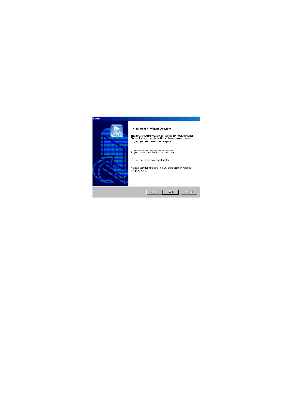
7. Once the Ins tall Shield W izard finishes updating your system, it
will prompt you to restart the computer. Tick on the Yes, I
want to restart my computer now followed by a click on the
Finish button to reboot. Only after your computer boots will the
new settings take effect.
NOTE:
WIN98/2K/XP IDE driver installations are the same.
47

5.2 VGA Driver Installation
5.2.1 Win 98
1. Ins ert Utility CD Disk into your CD ROM drive. The main menu will
pop up as shown below. Select on the HS-4706 button to launch
the installation program.
2. Click on the VGA Driver button to continue.
48

3. Click on the WIN9X button to continue.
4. When the dialog box below appea rs , m ake sure you close all
other Windows applications then click on the N
proceed.
ext > button to
49

5. The Intel OEM Software License Agreement dialog box then
appears on the screen. Choose Y
6. Once the setup program finishes copying files into yo ur system, it
will prompt you to restart the computer. Tick on the Yes, I want
to restart my computer now followed by a click on the F
button to reboot. Only after your computer boots will th e new
settings take effect.
es to proceed.
inish
50

5.2.2 Win NT
NOTE:
1. Ins ert Utility CD Disk into your CD ROM drive. The main menu will
2. Click on the VGA Driver button to continue.
3. Click on the WINNT button to continue.
Please make sure you have already installed Service Pack 6.0.
pop up as shown below. Select on the HS-4706 button to launch
the installation program.
51

4. When the dialog box below appea rs , m ake sure you close all
other Windows applications then click on the N
proceed.
5. The Intel OEM Software License Agreement dialog box then
appears on the screen. Choose Y
es to proceed.
ext > button to
52

6. Once the setup program finishes copying files into yo ur system, it
will prompt you to restart the computer. Tick on the Yes, I want
to restart my computer now followed by a click on the F
button to reboot. Only after your computer boots will th e new
settings take effect.
inish
5.2.3 Win 2000
1. I nsert Utility CD Disk into your CD ROM drive. The main menu will
pop up as shown below. Select on the HS-4706 button to launch
the installation program.
53

2. Click on the VGA Driver button to continue.
3. Click on the WIN2K button to continue.
54

4. When the dialog box below appea rs , m ake sure you close all
other Windows applications then click on the N
proceed.
5. The Intel OEM Software License Agreement dialog box then
appears on the screen. Choose Y
es to proceed.
ext > button to
55

6. Once the setup program finishes copying files into yo ur system, it
will prompt you to restart the computer. Tick on the Yes, I want
to restart my computer now followed by a click on the F
button to reboot. Only after your computer boots will th e new
settings take effect.
NOTE:
WINXP driver installation is the same as WIN2K.
inish
56

5.3 LAN Driver Installation
5.3.1 Win 98
1. Ins ert Utility CD Disk into your CD ROM drive. The main menu will
pop up as shown below. Select on the HS-4706 button to launch
the installation program.
2. Click on the LAN Driver button to continue.
57

3. Click on the WIN9X button to continue.
4. When the dialog box below appea rs , m ake sure you close all
other Windows applications then click on the Install Base
Driver button to proceed.
58

5. The Intel OEM Software License Agreement dialog box then
appears on the screen. Choose Accept to proceed.
6. Choose the drivers install location. (ex: c:\IntelPRO)
59

7. Once the setup program finishes copying files into yo ur system, it
will prompt you to restart the computer. Tick on the Restart
now to reboot. Only after your computer boots will the new
settings take effect.
5.3.2 Win NT
NOTE:
1. The system automatically detects the absence of Windows NT
2. Tick on the W
Please make sure you have already installed Service Pack 6.0.
Networking. Click on the Y
ired to the network once the following screen
appears. Click on the N
es button to start installation.
ext> to proceed.
60
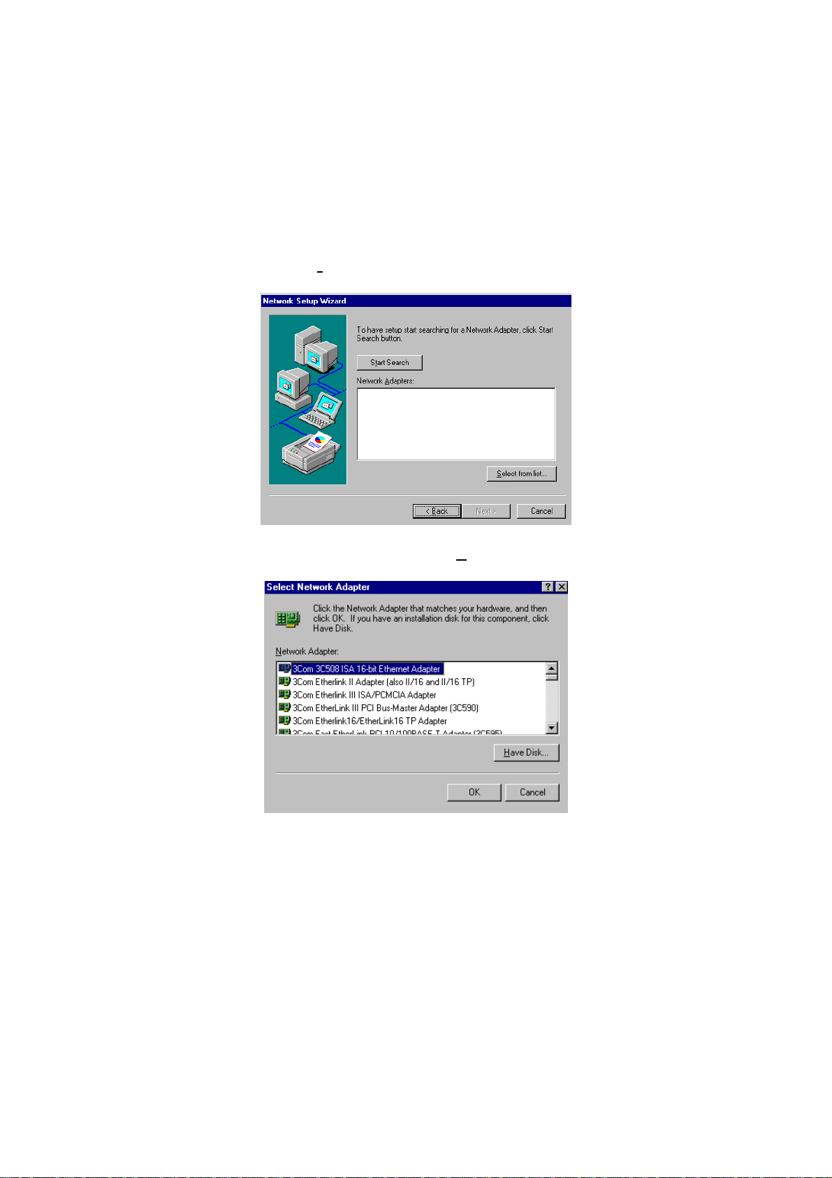
3. Click on the Start Search button for the program to l ocat e the
Network Adapter.
4. Once setup finishes the search, it will list a number of adapters
for you to choose from. Press on the H
the driver path location.
ave Disk button to assign
61

5. Setup now asks you for the location of the driver. When you have
entered the new driver path, press on the OK button to continue.
6. When Setup finds the information it needs about the new driver,
it will display the devic e it found on the following s creen. Please
choose “Intel(R) PRO/100 Family Adapter”. Press on the OK
button to accept and proceed.
7. Setup then returns to Network Setup Wizard screen and displays
your new Network Adapter. Click on N
ext to continue.
62

8. The Network Setup Wizard then al lo w s y ou to set the Netw o rk
Protocols on your network. Select the appropriate protocol and
then click on Next to continue.
9. Before Setup starts installing the components found and the
settings you made, it will give you the option to procee d or go
back for changes from the following screen. Click on the N
button once you are sure of your devices.
ext
63

10. Windows NT Setup will then need to copy files necessary to
update the system information. Specify the path then press
Continue.
11. When Setup asks if you wish to change the TCP/IP settings of
your system, select them appropriately. The default choice is N
12. Setup then starts the Networking installation and copies the files.
13. When the screen below appears, click on N
ext> to continue.
o.
64

14. Setup then prompts you that it is ready to start the network. You
may complete the installation thereafter. Click on N
continue.
15. Assign the workgroup or do m ain setting of your computer. Click
on Next to continue.
ext> to
65

16. When the dialog bo x below appears, it means your driver is install
completed. Click Finish button to proceed.
17. Click on the Y
installation for WIN NT4.0 is now complete.
es button to restart your computer. The LAN driver
66

5.3.3 WIN2K
1. Insert utility CD disk into your CD ROM drive. The main menu will
pop up as shown below. Select on the HS-4706 button to launch
the installation program.
2. Click on the LAN Driver button to continue.
67

3. Click on the WIN2K button to continue.
4. When the dialog box below appear s, m ake sure you close all
other Windows applications then click on the Install Base
Driver button to proceed.
68

5. The Intel OEM Software License Agreement dialog box then
appears on the screen, Choose Y
6. Choose driver instal l location. (ex: c:\IntelPRO)
es to proceed.
7. When setup is finished, please reboot your computer to
complete.
NOTE: WINXP driver installation is the same with WIN2K.
69

5.4 Audio Driver Installation
1. Ins ert Utility CD Disk into your CD ROM drive. The main menu will
pop up as shown below. Select on the HS-4706 button to launch
the installation program.
2. Click on the Audio Driver button to continue.
70

3. Choose on the OS button to continue.
4. When the dialog box below appea rs , m ake sure you close all
other Windows applications then click on the N
proceed.
ext > button to
4. Once the InstallShi e ld Wizard completes the operation an d
update of your AC’97 driver, it w ill ask you to remove disks from
their drives, and prompt you to restart your system. Tick on the
Yes, I want to restart my computer now. Afterwards, click on the
F
inish button to complete the installation process. The system
changes you made will take effect after the system restarts.
71

NOTE:
WIN98/2K/NT audio driver installations are the same as WINXP.
5.5 USB2.0 Driver Installation
5.5.1 Win 98
1. With the Utility C D Dis k s til l in y ou r C D R O M d r ive , r ig ht c lic k on
“My Computer” icon from the Windows menu. Select on System
Properties and then proceed to the Device Manager from the
main menu.
72

2. Select on Other Devices from the list of devices then double-click
on PCI Universal Serial Bus.
3. The PCI Universal Serial Bus Properties screen then appears,
allowing you to re-inst all the dr iver . Selec t Driver from the main
menu to proceed.
73

4. When the dialog box below appea rs , m ake sure you close all
other Windows applications then click on the N
proceed.
5. Tick on the “Search for a better driver” once the follo wing sc reen
appears. Click on the N
ext to proceed.
ext > button to
74

6. Once the program returns to the Add New Hardware Wizard
screen, your specified location will appear. Press on the N
button to continue
7. When Setup finds the information it needs about the new driver,
it will display the device it found on the following screen. Press on
the N
ext button to accept and proceed.
ext
75

8. Once the InstallShi e ld Wizard completes the operation an d
update of your USB2.0 driver. Click on the F
complete the installation process.
inish button to
5.5.2 Win 2000
1. With the Utility C D Dis k s til l in y ou r C D R O M d r ive , r ig ht c lic k on
“My Computer” icon from the Windows menu. Select on System
Properties and then proceed to the Device Manager from the
main menu.
2. Select on Other Devices from the list of devices then double-click
on PCI Universal Serial Bus.
76

3. The PCI Universal Serial Bus Properties screen then appears,
allowing you to re-inst all the dr iver . Selec t Driver from the main
menu to proceed.
4. When the dialog box below appears, make sure you close all
other Windows applications then click on the N
proceed.
ext > button to
77

5. Tick on the “Search for a suitable driver” once the following
screen appears. Click on the N
6. Once the program returns to the Add New Hardware Wizard
screen, your specified location will appear. Press on the N
button to continue
ext to proceed.
ext
78

7. Choose the driver disk location.
8. Once the InstallShi e ld Wizard completes the operation an d
update of your USB2.0 driver. Click on the F
complete the installation process.
inish button to
79

5.5.3 Win XP
1. Ins ert Utility CD Disk into your CD ROM drive. The main menu will
pop up as shown below. Select on the HS-4706 button to launch
the installation program.
2. Click on the USB2.0 Driver button to continue.
80

3. Click on the WINXP button to continue.
4. When the dialog box below appea rs , m ake sure you close all
other Windows applications then click on the N
proceed.
ext > button to
81

5. Once the InstallShi e ld Wizard completes the operation an d
update of your USB2.0 driver. Click on the F
complete the installation process.
inish button to
82
 Loading...