

Page 1

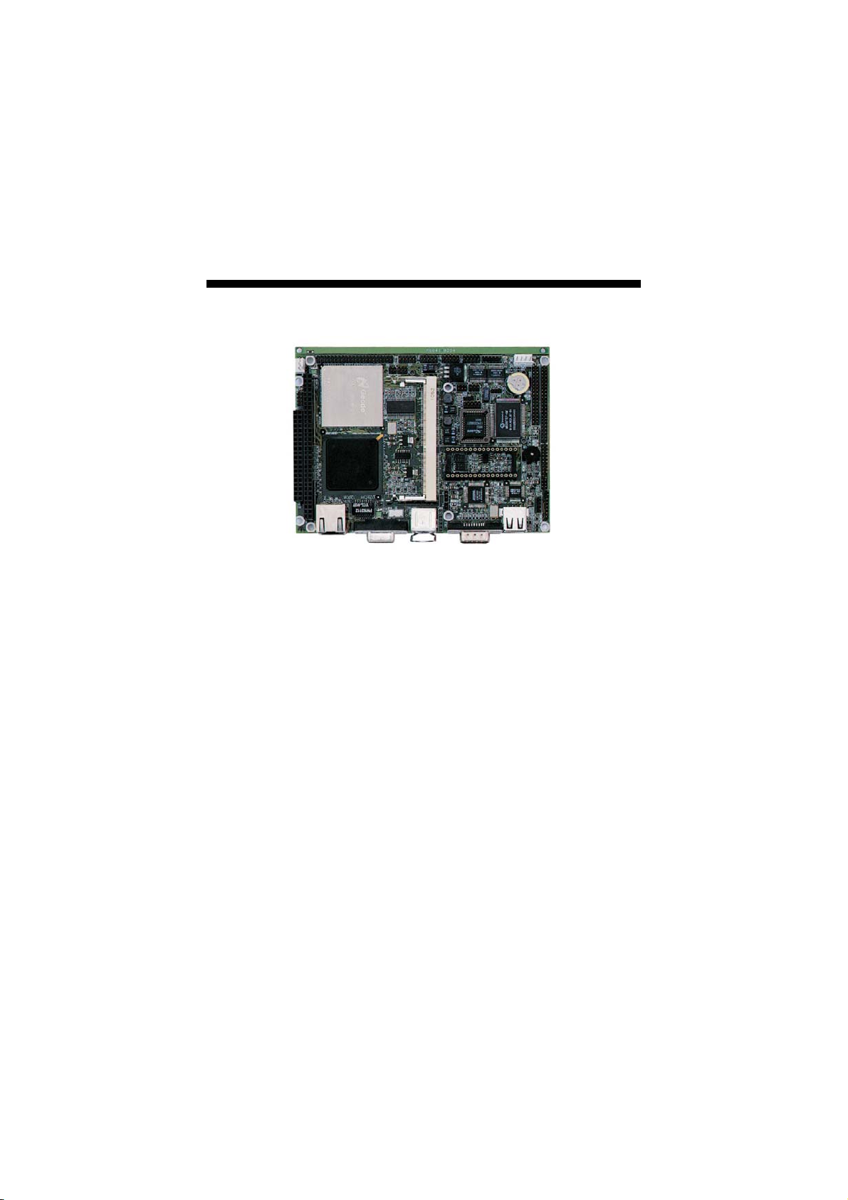
HS-2603
Geode GX1 Embedded Board with
CompactFlash, VGA, Audio & LAN
•300MHz•SODIMM•CompactFlash•Mini PCI•
•
CRT/Panel•LAN•Audio•4COM•PC/104•IrDA•
•RS-232/422/485•USB•DiskOnChip•WDT•Single +5V•
Page 2

Copyright Disclaimers
The accuracy of contents in this manual has passed thorough checking and review
before publishing. BOSER Technology Co., Ltd., the manufacturer and publisher, is
not liable for any infringements of patents or other rights resulting from its use. The
manufacturer will not be responsible for any direct, indirect, special, incidental
or consequential damages arising from the use of this product or
documentation, even if advised of the possibility of such damage(s).
This manual is copyrighted and BOSER Technology Co., Ltd. reserves all
documentation rights. Unauthorized reproduction, transmission, translation,
and storage of any form and means (i.e.,
recording) of this document, in whole or partly, is prohibited, unless granted
permission by BOSER Technology Co., Ltd.
BOSER Technology Co., Ltd. reserves the right to change or improve the
contents of this document without due notice.
assumes no responsibility for any errors or omissions that may appear in this
manual, nor does it make any commitment to update the information contained
herein.
T
r
a
d
e
m
a
r
k
s
T
r
a
d
e
m
T
r
a
d
e
m
BOSER is a registered trademark of BOSER Technology Co., Ltd.
ISB is a registered trademark of BOSER Technology Co., Ltd.
Intel is a registered trademark of Intel Corporation.
Award is a registered trademark of Award Software, Inc.
All other trademarks, products and or product names mentioned herein are
mentioned for identification purposes only, and may be trademarks and/or
registered trademarks of their respective companies or owners.
a
r
k
s
a
r
k
s
electronic, mechanical, photocopying,
BOSER Technology Co., Ltd.
© Copyright 2003 BOSER Technology Co., Ltd.
All Rights Reserved.
Version 1.4, July 28, 2003
Page 3

Table of Contents
Chapter 1 General Description ---------------------------------1
1.1 Major Features ------------------------------------------------------ 2
1.2 Specifications ------------------------------------------------------- 3
1.3 Board Dimensions ------------------------------------------------- 4
Chapter 2 Unpacking ---------------------------------------------5
2.1 Opening the Delivery Package--------------------------------- 5
2.2 Inspection------------------------------------------------------------- 5
Chapter 3 Hardware Installation-------------------------------7
3.1 Before Installation-------------------------------------------------- 7
3.2 Board Layout -------------------------------------------------------- 8
3.3 Jumper List----------------------------------------------------------- 9
3.4 Connector List ------------------------------------------------------ 9
3.5 Configuring the CPU -------------------------------------------- 10
3.6 System Memory--------------------------------------------------- 10
3.7 DiskOnChip Address Setting ------------------------------ 11
JP9 (1-4): DiskOnChip Address Select ----------11
3.7.1 Installing DiskOnChip Modules--------------------------------11
3.7.1 Removing DiskOnChip Modules ------------------------------ 12
3.8 VGA Controller ---------------------------------------------------- 13
JP1: Panel Voltage Select --------------------------13
CN6: 15-pin CRT Connector (DB15) ---------------13
CN5: 44-pin Panel Connector ---------------------14
3.9 PCI E-IDE Drive Connector------------------------------------ 15
CN16: Primary IDE Connector ---------------------15
3.10 Floppy Disk Drive Connector--------------------------------- 16
CN15: FDD Connector ------------------------------ 16
3.11 Serial Port Connectors ----------------------------------------- 16
CN13: COM1 Connector (DB9) --------------------16
CN12, CN9 and CN11: COM2/COM3/COM4
Connectors (5x2 Header) -------------------------- 17
CN7: RS-422/485 Connector (5x2 Header) -------17
JP2: RS-422/485 Receiver
Enabled/Disabled Select --------------------------17
JP3: RS-422/485 Transceiver
Enabled/Disabled Select --------------------------17
JP6, JP8: RS-232 or RS-422/485 Selection --------- 17
3.12 Parallel Connector ----------------------------------------------- 18
CN17: Parallel Connector -------------------------- 18
3.13 Ethernet Connector---------------------------------------------- 18
CN4: RJ-45 and LAN LED Connector --------------18
3.14 IrDA Connector --------------------------------------------------- 19
JP10: IrDA Connector-------------------------------19
Page 4

3.15
USB Connector --------------------------------------------------- 19
3.16 CMOS Data Clear ------------------------------------------------- 19
3.17 Power and Fan Connectors ----------------------------------- 20
3.18 Keyboard/Mouse Connectors -------------------------------- 20
3.19 Front Panel Signal Connector-------------------------------- 21
3.20 Audio Connector ------------------------------------------------- 21
3.21 TV Out Function -------------------------------------------------- 21
3.22 Watchdog Timer -------------------------------------------------- 22
3.23 CompactFlash Connector ----------------------------------- 24
3.24 Mini PCI Connector ---------------------------------------------- 25
3.25 PC/104 Connectors ---------------------------------------------- 27
JP12 and JP13: USB Connectors ------------------- 19
JP11: Clear CMOS ----------------------------------19
CN14: 4-pin Power Connector---------------------20
FN1: FAN Connector-------------------------------- 20
CN8: 6-pin PS/2 Mini DIN Keyboard/Mouse
Connector------------------------------------------- 20
CN10: 6-pin Keyboard/Mouse Connector--------20
CN1: Front Panel Signal Connector ---------------21
JP14: Line In/Line Out/Mic In Connector---------- 21
JP5: S-Video Output --------------------------------21
JP4: Composite Video Output ---------------------22
JP7: Watchdog Timer Active Type Setting ------- 22
JP9 (5-10): WDT Period Select---------------------- 22
J1: CompactFlash Connector -------------------24
PC1: Mini PCI Connector Pin Information ---------25
CN2: 40-pin PC/104 Expansion Slot ---------------27
CN3: 64-pin PC/104 Expansion Slot ---------------28
Chapter 4 Award BIOS Setup -------------------------------- 29
4.1 Starting Setup ----------------------------------------------------- 29
4.2 Using Setup -------------------------------------------------------- 30
4.2.1 Getting Help---------------------------------------------------------- 30
4.3 Main Menu ---------------------------------------------------------- 31
4.4 Standard CMOS Setup------------------------------------------ 33
4.5 BIOS Features Setup -------------------------------------------- 36
4.6 Chipset Features Setup ---------------------------------------- 40
4.7 Power Management Setup ------------------------------------ 42
4.7.1 PM Timers -------------------------------------------------------------43
4.7.2 Reload Global Timer Events --------------------------------------44
4.8 PNP/PCI Configuration ----------------------------------------- 45
4.9 Load BIOS Defaults---------------------------------------------- 47
4.10 Load Setup Defaults--------------------------------------------- 48
4.11 Integrated Peripherals ------------------------------------------ 49
4.12 Supervisor/User Password Setting------------------------- 52
4.13 IDE HDD Auto Detection --------------------------------------- 53
4.14 Save & Exit Setup ------------------------------------------------ 54
4.15 Exit Without Saving---------------------------------------------- 55
Page 5

Chapter 5 Software Utilities ----------------------------------- 57
5.1 VGA Driver Installation for WIN95 & WIN98 ------------- 57
5.2 VGA Driver Installation for WIN NT4.0--------------------- 59
5.3 Network Driver Installation for WIN98 --------------------- 61
5.4 Network Driver Installation for WIN NT4.0 --------------- 63
5.5 Audio Driver Installation for WIN NT4.0------------------- 67
Page 6

Safety Instructions
Integrated circuits on computer boards are sensitive to static electricity.
To avoid damaging chips from electrostatic discharge, observe the
following precautions:
Do not remove boards or integrated circuits from their anti-static
packaging until you are ready to install them.
Before handling a board or integrated circuit, touch an unpainted portion
of the system unit chassis for a few seconds. This helps to discharge any
static electricity on your body.
Wear a wrist-grounding strap, available from most electronic component
stores, when handling boards and components. Fasten the ALLIGATOR
clip of the strap to the end of the shielded wire lead from a grounded
object. Please wear and connect the strap before handle the HS-2603 to
ensure harmlessly discharge any static electricity through the strap.
Please use an anti-static pad when putting down any components or
parts or tools outside the computer. You may also use an anti-static bag
instead of the pad. Please inquire from your local supplier for additional
assistance in finding the necessary anti-static gadgets.
NOTE:
DO NOT TOUCH THE BOARD OR ANY OTHER SENSITIVE
COMPONENTS WITHOUT ALL NECESSARY ANTI-STATIC
ROTECTION.
Page 7
Chapter 1
General Description
The HS-2603 is a Mini PCI Local Bus Embedded SBC. The board
combines the necessary input and output interfaces to make it an ideal
all-in-one industrial single board computer.
The HS-2603 provides one set of PC/104 connector for 16-bit ISA bus.
The board is also designed with a low power Cyrix
300MHz CPU and audio interface which provides an ideas sound
adapter in any sound application. The IDE interface with ATA/33
access of mode 4 to IDE drive interface architecture, supports a
maximum 33MB/sec in data transfer rating to two IDE drive connection
and provides onboard one 10/100 based LAN for easy network
connection.
A single Flash chip holds the system BIOS, and you can change the
Flash BIOS by the Utility Update. Advanced IR port also provides a
faster data transmission. You can also use the DOS version of the
"DiskOnChip" socket by issuing commands from the DOS prompt
without the necessity of other software supports up to 288MB.
The board comes with Cyrix
connections to CRT or Panel display. The VGA uses shared memory of
4MB.
The HS-2603 provides with one SO-DIMM socket provides up to
128MB of main system memory.
®
CX5530 VGA and provides internal
®
Geode GX1
1
Page 8
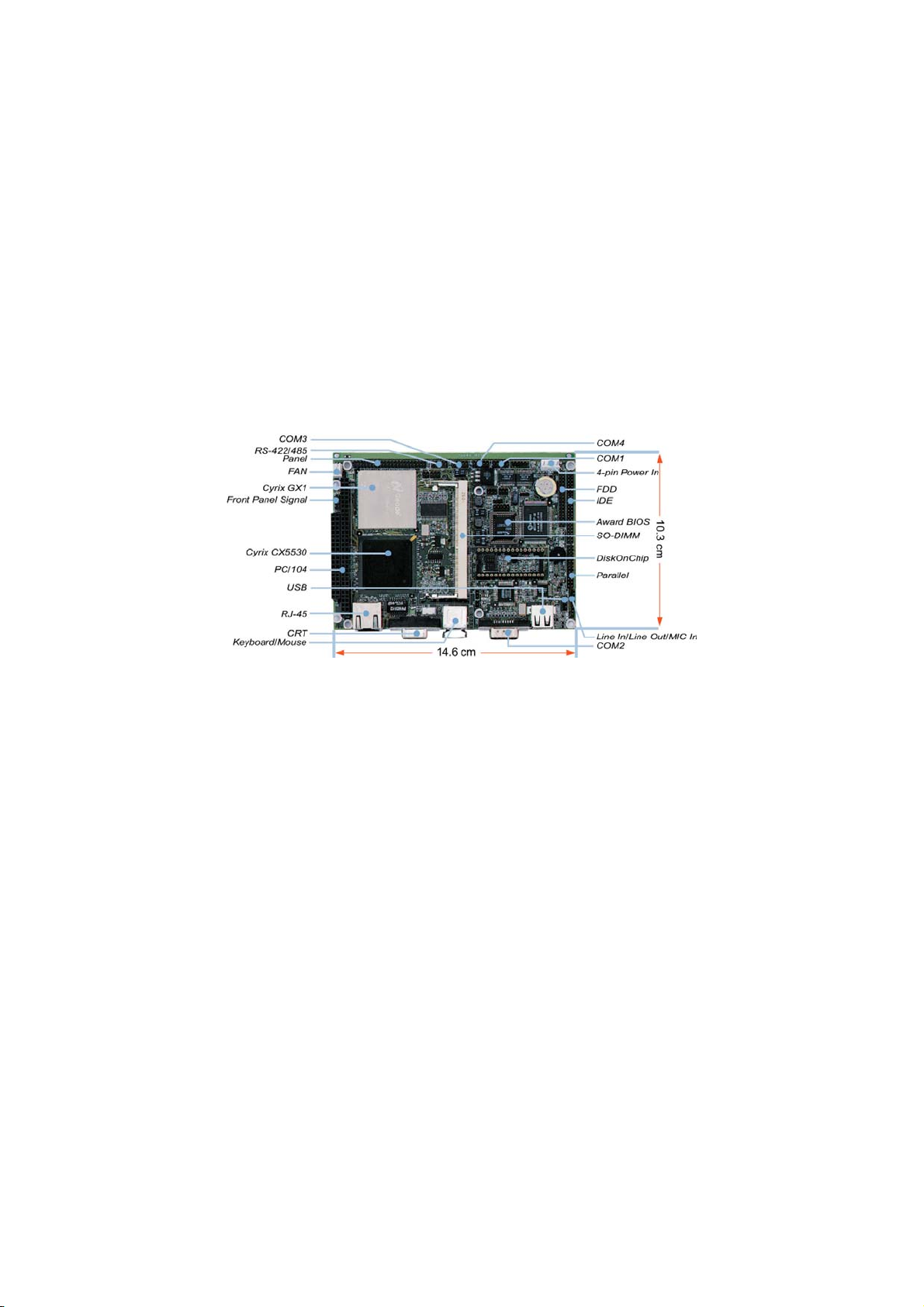
To ensure the reliability in an unmanned or standalone system
, the
Watchdog Timer (WDT) onboard HS-2603 is designed with pure
hardware that does not need the arithmetical functions of a real-time
clock chip. If any program causes unexpected halts to the system, the
onboard Watchdog Timer (WDT) will automatically reset the CPU or
generate an interrupt to resolve such condition. The HS-2603 also has
a CompactFlash connector that accommodates standard
CompactFlash memory cards available in the market.
1.1 Major Features
The HS-2603 comes with the following features:
Cyrix Geode GX1 300MHz CPU
Mini PCI Local Bus support
Cyrix GX1, CX5530 system chipset
One SO-DIMM socket with a max. capacity of 128MB
SMC 37C669 and Winbond W83977 super I/O chipset
Three RS-232 and one RS-232/422/485 serial ports
PC/104 Bus connector
Cyrix CX5530 CRT/Panel display controller
RealTek RTL8100 10/100 Based LAN
Cyrix CX5530 3D audio controller
DiskOnChip socket supporting memory sizes of up to 288MB
Supports CompactFlash card reader
Supports Single +5V power in
2
Page 9

1.2 Specifications
CPU: Cyrix Geode GX1 300MHz Low Power CPU
Bus Interface: Mini PCI Local Bus
Memory: One SO-DIMM socket supporting up to 128MB
Chipset: Cyrix Geode GX1 and Cyrix CX5530
I/O Chipset: Winbond W83977 and SMC 37C669
CompactFlash: One standard Compact Flash adapter onboard (solder
side)
FDD: Supports up to two floppy disk drives
PC/104: PC/104 connector for 16-bit ISA Bus
IrDA: One IrDA TX/RX header
Cyrix CX5530 with 4MB shared main memory supporting
VGA:
CRT/Panel displays up to 1024 x 768 at 16-bit colors
IDE: Two IDE disk drives supporting ATA/33 and with a transfer rate up to
33MB/sec.
Parallel:
SPP/ECP/EPP
LAN: RealTek RTL8100 10/100 Based LAN
Audio: Cyrix CX5530 3D audio controller
Serial Port: 16C550 UART-compatible RS-232/422/485 x 1 and RS-232 x
3 serial ports with 16-byte FIFO
USB:
TV-Out:
Keyboard/Mouse:
DiskOnChip: DiskOnChip socket supporting memory sizes of up to
288MB
BIOS: Award PnP Flash BIOS
Watchdog Timer: Sets 1, 2, 10, 20, 110, 220 seconds activity trigger with
Reset or NMI
CMOS:
DMA Channels:
Interrupt Levels:
Power: Single +5V power in
Operating Temperature: 0~60 oC
Board Size: 14.6 x 10.3 cm
One enhanced bi-directional parallel port supporting
Two USB connectors
Supports PAL and NTSC systems (optional)
PS/2 6-pin Mini DIN or 6-pin connector
Battery backup
7
15
3
Page 10
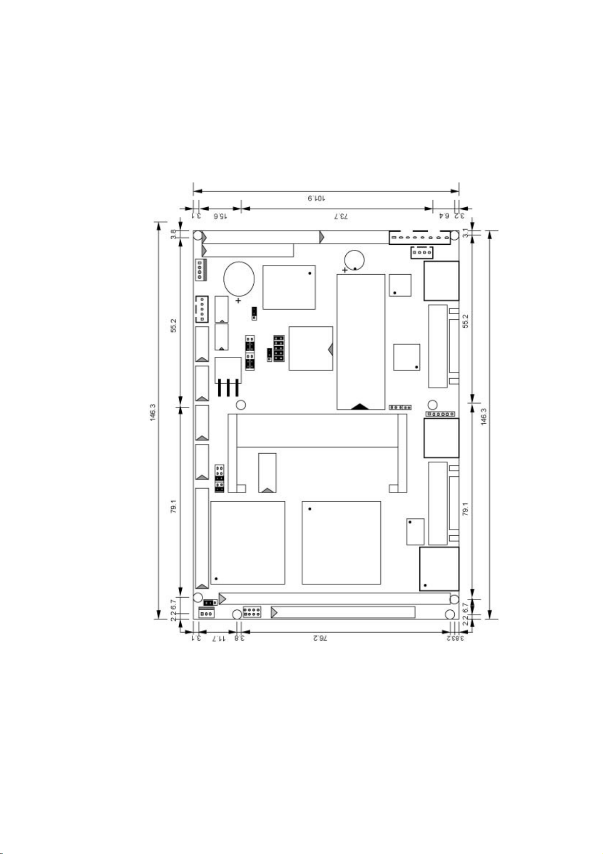
1.3 Board Dimensions
4
Page 11

Chapter 2
Unpacking
2.1 Opening the Delivery Package
The HS-2603 is packed in an anti-static bag. The board has
components that are easily damaged by static electricity. Do not
remove the anti-static wrapping until proper precautions have been
taken. Safety Instructions in front of this manual describe anti-static
precautions and procedures.
2.2 Inspection
After unpacking the board, place it on a raised surface and carefully
inspect the board for any damage that might have occurred during
shipment. Ground the board and exercise extreme care to prevent
damage to the board from static electricity.
Integrated circuits will sometimes come out of their sockets during
shipment. Examine all integrated circuits, particularly the BIOS,
processor, memory modules, ROM-Disk, and keyboard controller chip
to ensure that they are firmly seated. The HS-2603 delivery package
contains the following items:
HS-2603 Industrial Single Board Computer
IDE port Flat Cable x 1
FDD Port Flat Cable x 1
PS/2 Keyboard/Mouse Transfer Cable x 1
Printer Port Flat Cable x 1
COM Port Flat Cable x 3
USB Port Flat Cable x 1
Sound connector Cable x 1
Utility Disc x 1
User’s Manual
5
Page 12

It is recommended that you keep all the parts of the delivery package
intact and store them in a safe/dry place for any unforeseen event
requiring the return shipment of the product. In case you discover any
missing and/or damaged items from the list of items, please contact
your dealer immediately.
6
Page 13

Chapter 3
Hardware Installation
This chapter provides the information on how to install the hardware
using the HS-2603. This chapter also contains information related to
jumper settings of switch, watchdog timer, and the DiskOnChip
address selection etc.
3.1 Before Installation
After confirming your package contents, you are now ready to install
your hardware. The following are important reminders and steps to
take before you begin with your installation process.
1. Make sure that all jumper settings match their default settings
and CMOS setup correctly. Refer to the sections on this chapter
for the default settings of each jumper.
2. Go through the connections of all external devices and make
sure that they are installed properly and configured correctly
within the CMOS setup. Refer to the sections on this chapter
for the detailed information on the connectors.
3. Keep the manual and diskette in good condition for future
reference and use.
Warning:
Before using the HS-2603, set the CMOS jumper JP11 setting to
Short 1-2 in order to connect the battery. Not doing so will cause
the CMOS to be lost.
7
Page 14
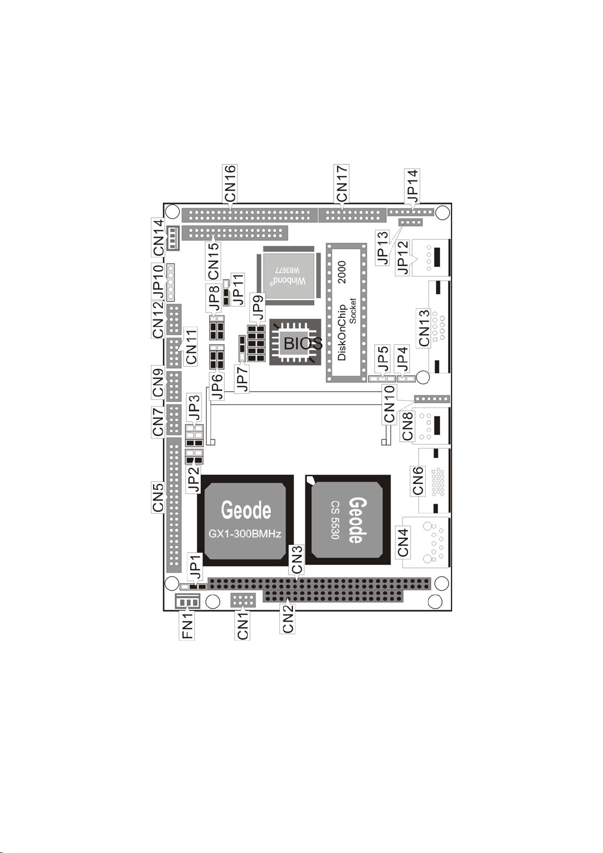
3.2 Board Layout
8
Page 15
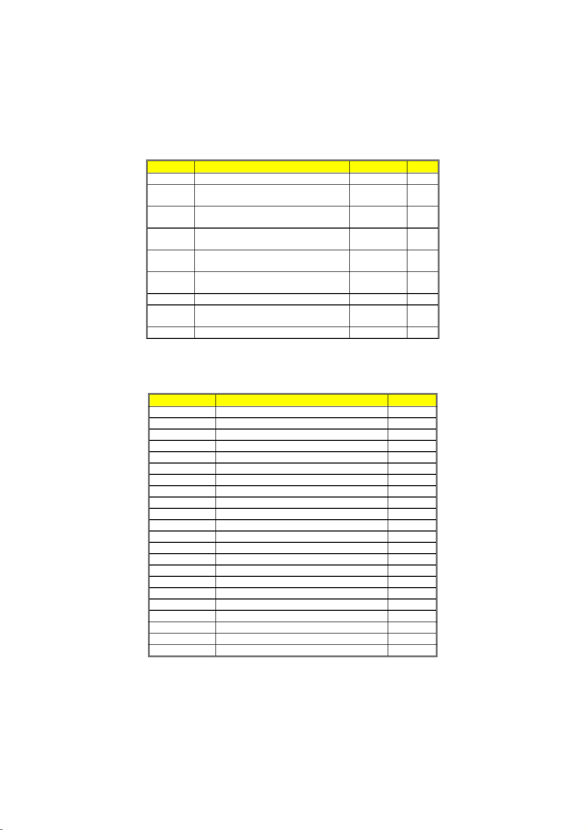
3.3 Jumper List
Jumper Definition Default Page
JP1 Panel Voltage Select: 3.3V Short 2-3 13
JP2
JP3
JP6
JP7
JP8
JP9 (1-4) DiskOnChip Address Select: D000 Short 1-2, 3-4 11
JP9 (5-10) Watchdog Timer Period Select: 1 sec. Short 5-6, 7-8,
JP11 Clear CMOS: Clear CMOS Short 2-3 19
Important:
RS-422/485 Receiver
Enabled/Disabled Select: Auto
RS-422/485 Transceiver
Enabled/Disabled Select: Auto
RS-232 or RS-422/485
Enabled/Disabled Select: RS-232
Watchdog Timer Active Type Select:
System Reset
RS-232 or RS-422/485
Enabled/Disabled Select: RS-232
The default battery setting for JP11 is Short 2-3. Please set
JP11 to Short 1-2 when you start up your system.
Short 1-2 17
Short 1-2 17
Short 1-2, 2-4 17
Short 2-3 22
Short 1-3, 2-4 17
22
9-10
3.4 Connector List
Connector Definition Page
CN1 Front Panel Signal Connector 21
CN2
CN3 PC/104 64-pin Connector 28
CN4 RJ45 and LAN LED Connector 18
CN5 Panel Connector 14
CN6 CRT Connector 13
CN7
CN8 PS/2 6-pin Mini DIN KB/Mouse Connector 20
CN9 COM3 (5x2 header) 17
CN10 6-pin Keyboard/Mouse Connector 20
CN11 COM4 (5x2 header) 17
CN12 COM2 Connector (5x2 Header) 17
CN13 COM1 Connector (DB9) 16
CN14
CN15 Floppy Connector 16
CN16 IDE Connector 15
CN17 Parallel Connector 18
FN1 Fan Connector 20
J1
JP4 Composite Video Output 22
JP5
JP10 IrDA Connector 19
PC104 40-pin Connector 27
RS-422/485 Connector (5x2 header) 17
4-pin Power In Connector 20
CompactFlash Connector 24
S-Video Output 21
. . . More on next page . . .
9
Page 16
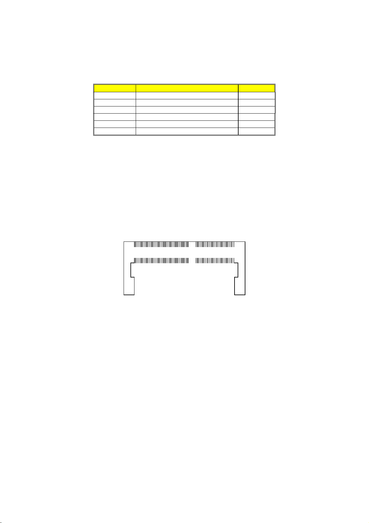
Connector Definition Page
JP12
JP13 USB Connector 19
JP14 Line In / Line Out / Mic In Connector 21
PC1 Mini PCI Connector 25
U6 SO-DIMM Socket 10
U10 DiskOnChip Socket 11
USB Connector 19
3.5 Configuring the CPU
The HS-2603, with its onboard BGA processor, auto-detects the
features of the mounted microprocessor onboard. The HS-2603
automatically identifies the frequency and clock speed of the installed
microprocessor chip, thereby eliminating the need for user to do
additional CPU configuration or hardware settings related to it.
3.6 System Memory
The HS-2603 provides one SO-DIMM socket at location U6. This
onboard memory socket can support 64MB, and 128MB SO-DIMM
modules. The system’s maximum memory capacity is 128MB.
143
144 2
1
NOTE:
10
144-pin SO-DIMM Socket
pin orientation
SO-DIMM sockets out on the market these days have very fragile
contacts that attach to modules. We highly recommend you not to
regularly remove the installed SO-DIMM from its socket. Doing so
may wear out the contact between the socket and module.
Page 17
3.7 DiskOnChip Address Setting
The DiskOnChip function allows the system to boot or operate
without a FDD or a HDD. DiskOnChip modules may be formatted as
drive C. With DiskOnChip, user may also execute DOS commands
such as FORMAT, SYS, COPY, XCOPY, DISCOPY and DISKCOMP
etc.
The U10 location onboard the HS-2603 is the DiskOnChip module
socket. If you have another memory device that has a similar memory
capacity with that of the DOC in your system, please set both at
different memory address mapping to avoid mapping area conflicts.
Failing to do so will not make the HS-2603 and the additional memory
device function properly. JP9 (1-4) selects the starting memory
address of the DiskOnChip (D.O.C.) to avoid the mapping area with
any other memory devices.
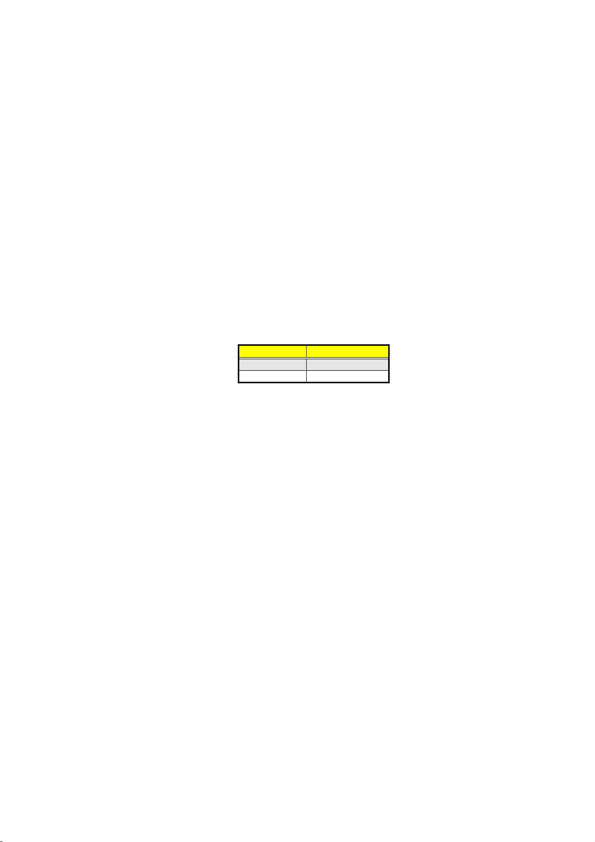
JP9 (1-4): DiskOnChip Address Select
Address JP9 (1-4)
* D000 Short 1-2, 3-4
D800 Short 3-4
3.7.1 Installing DiskOnChip Modules
When installing a DiskOnChip module onto your board, please take
note of the following:
1. Orient yourself properly with the location of the DiskOnChip
socket. Try to locate the pin 1 location on your socket. Pin
numbers are usually printed on either the component side or the
solder side of your board.
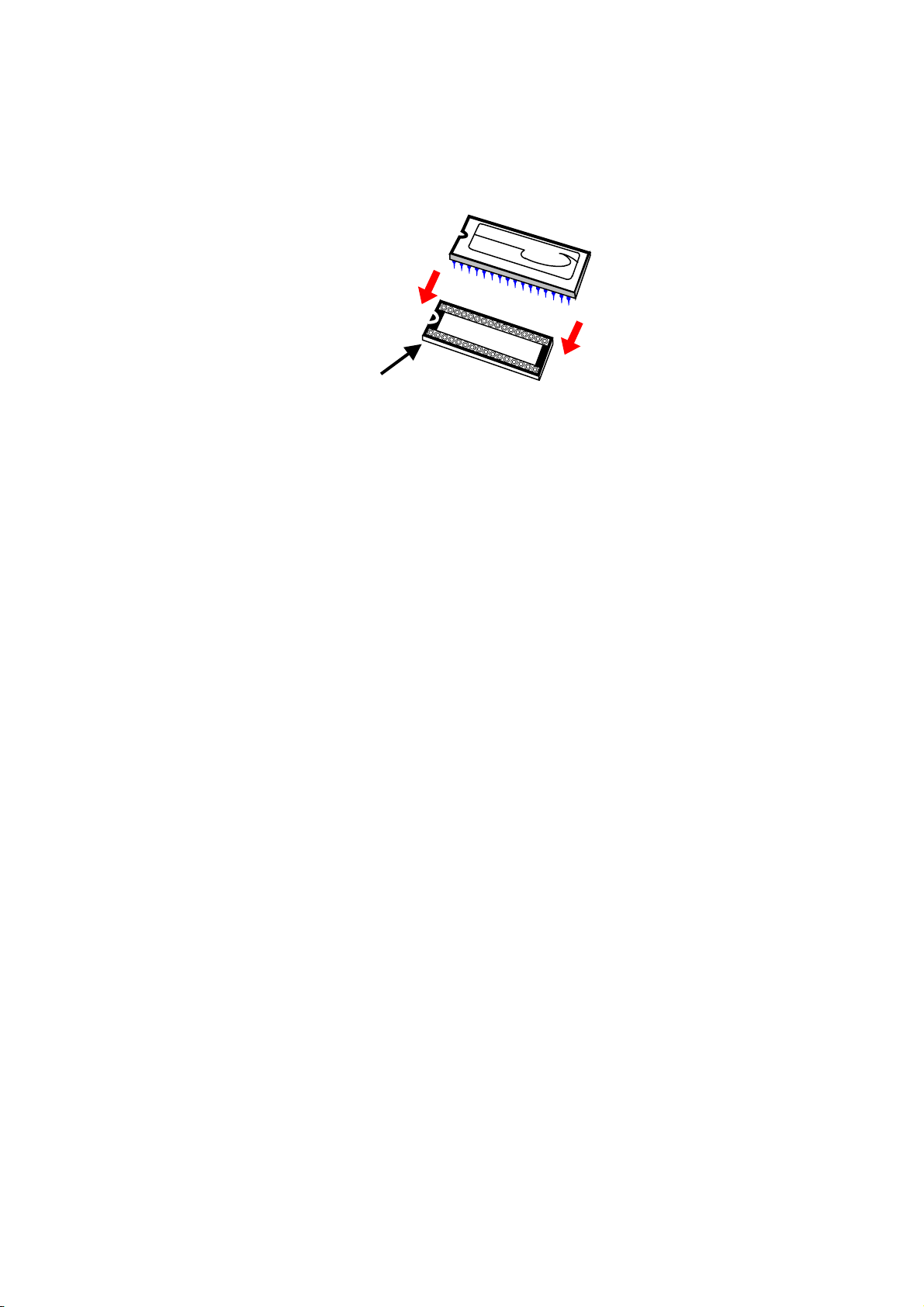
2. Locate the Pin 1 location on your DiskOnChip module. More
often than not, Pin 1 can be found on the lower right corner of
the chip. Please refer to the diagram for the exact location.
3. Once you have figured out where the pin 1 locations are on both
chip and socket, align the module’s pins on an upright angle
against the socket. Using both thumbs, gently press the module
into the socket until all the pins are secured to their
designations.
11
Page 18
D
i
s
k
O
n
C
h
i
p
Pin 1
Location
4. The installation is now complete and your module is now ready
for use.
NOTE:
If you encounter difficulty installing your DiskOnChip
module,
please consult a qualified technician or engineer to perform the
installation.
3.7.1 Removing DiskOnChip Modules
When removing a DiskOnChip module from its socket, please take
note of the following:
1. Loosen the contact of the module from its socket using a
screwdriver.
2. Insert the screwdriver’s flat head into a gap on either end of the
socket. Do not insert the screwdriver head on either side where
the pins are located. Doing so might damage the pins in the
process.
3. Slowly lift the screwdriver handle upwards. This will disengage
the module from its socket.
NOTE:
If you encounter difficulty removing your DiskOnChip
please consult a qualified technician or engineer to remove it for
you.
module,
12
Page 19
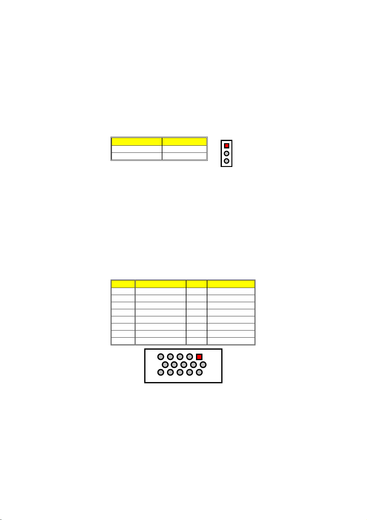
3.8 VGA Controller
The HS-2603 has an onboard jumper that selects the working voltage
of the flat panel connected to the system. Jumper JP1 offers two
voltage settings for the user.
JP1: Panel Voltage Select
Options Settings
5.0 V Short 1-2
3.3 V (default) Short 2-3
WARNING:
Please contact the supplier of your panel and make sure of the correct
voltage it uses. Incorrect settings on JP1 may cause internal damage to
your panel.
The onboard Cyrix® CX5530 chipset provides 4MB shared memory
VGA that supports up to 1024x768x16M colors resolution. The board
allows user to auto disable the VGA if another ISA bus display card is
plugged into the ISA slot. There is no need to set any jumper to disable
the onboard VGA if any 2nd ISA bus VGA card is plugged in into the
ISA slot. When using a PCI VGA card, the BIOS of HS-2603 allow the
user to select an external PCI VGA card or the onboard VGA function.
The HS-2603 provides two connection methods of a VGA device. CN6
offers a single standard CRT connector (DB15) while CN5 is the 44-pin
panel connector onboard reserved for flat panel installation.
CN6: 15-pin CRT Connector (DB15)
PIN Description PIN Description
1 Red 2 Green
3 Blue 4 N/C
5 GND 6 GND
7 GND 8 GND
9 VCC 10 GND
11
13 HSYNC 14 VSYNC
15 SCL
N/C
1
2
3
12
DDCSPA
IMPORTANT:
5
10
15
1
6
11
In connecting the cable for CN6, note that the connector
cannot be shifted nor connected in the wrong direction in
order not to damage the board.
13
Page 20
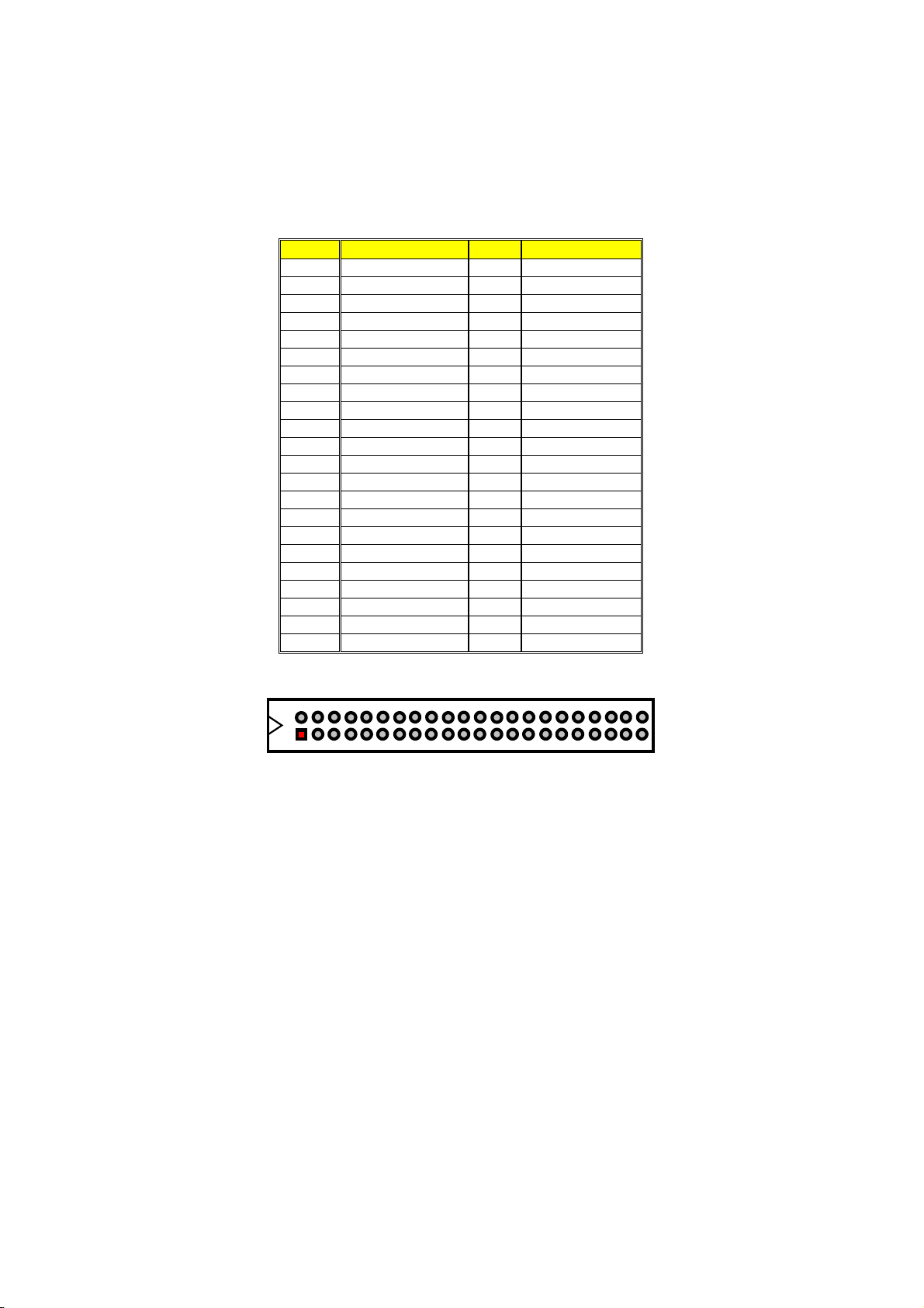
CN5: 44-pin Panel Connector
PIN Description PIN Description
1 +12V 2 +12V
3 GND 4 GND
5 3.3V / 5V
7
9 N/C 10 N/C
11 FPD0 12 FPD1
13 FPD2 14 FPD3
15 FPD4 16 FPD5
17 N/C 18 N/C
19 FPD6 20 FPD7
21 FPD8 22 FPD9
23 FPD10 24 FPD11
25 N/C 26 N/C
27 FPD12 28 FPD13
29 FPD14 30 FPD15
31
33 N/C 34 N/C
35 SHFCLK 36 FPVSYNC
37 FPDISPEN 38 FPHSYNC
39 GND 40 FPBKLEN
41 N/C 42 N/C
43 N/C 44 N/C
N/C
FPD16
Note
6 FPVDDEN
8
32
GND
FPD17
NOTE:
14
46810 182022242628303212 14 16 34 36 38 40 42 44
2
1
3 5 7 9 11 19 21 23 25 27 29 31 33 3513 15 17 37 39 41 43
Please set the proper voltage of your panel using JP1 before
proceeding on installing it.
Page 21
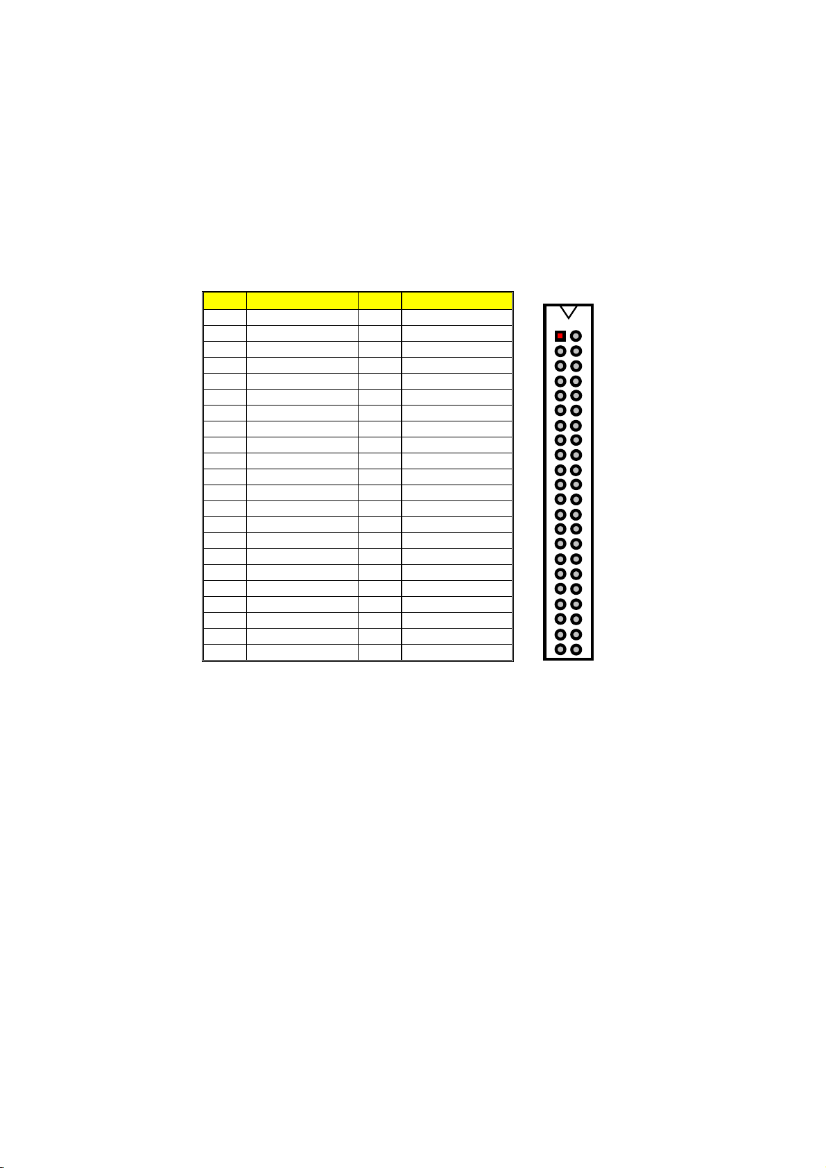
3.9 PCI E-IDE Drive Connector
CN16, a 44-pin connector, provides the PCI E-IDE drive provisions
onboard. A maximum of two IDE drives may be connected on them.
CN16: Primary IDE Connector
PIN Description PIN Description
1 BRSTDRVJ 2 GND
3 DD7-1 4 DD8-1
5 DD6-1 6 DD9-1
7 DD5-1 8 DD10-1
9
DD4-1
10
DD11-1
11 DD3-1 12 DD12-1
13 DD2-1 14 DD13-1
15 DD1-1 16 DD14-1
17 DD0-1 18 DD15-1
19 GND 20 N/C
21 DRQ 22 GND
23 RPDIOW- 24 GND
25 RPDIOR- 26 GND
27 N/C 28 ALE
29 RPDACK- 30 GND
31 IRQ14 32 IOCS16
33
RPDA1-
34
N/C
35 RPDA0- 36 RPDA2-
37 CS0 38 CS1
39 HLED 40 GND
41 VCC 42 VCC
43 GND 44 GND
1
2
46810
1214
1636
18
20
22
2426
28
30
3234
38
39 3579171921232527293133 1113153537
41
43
40
42
44
15
Page 22
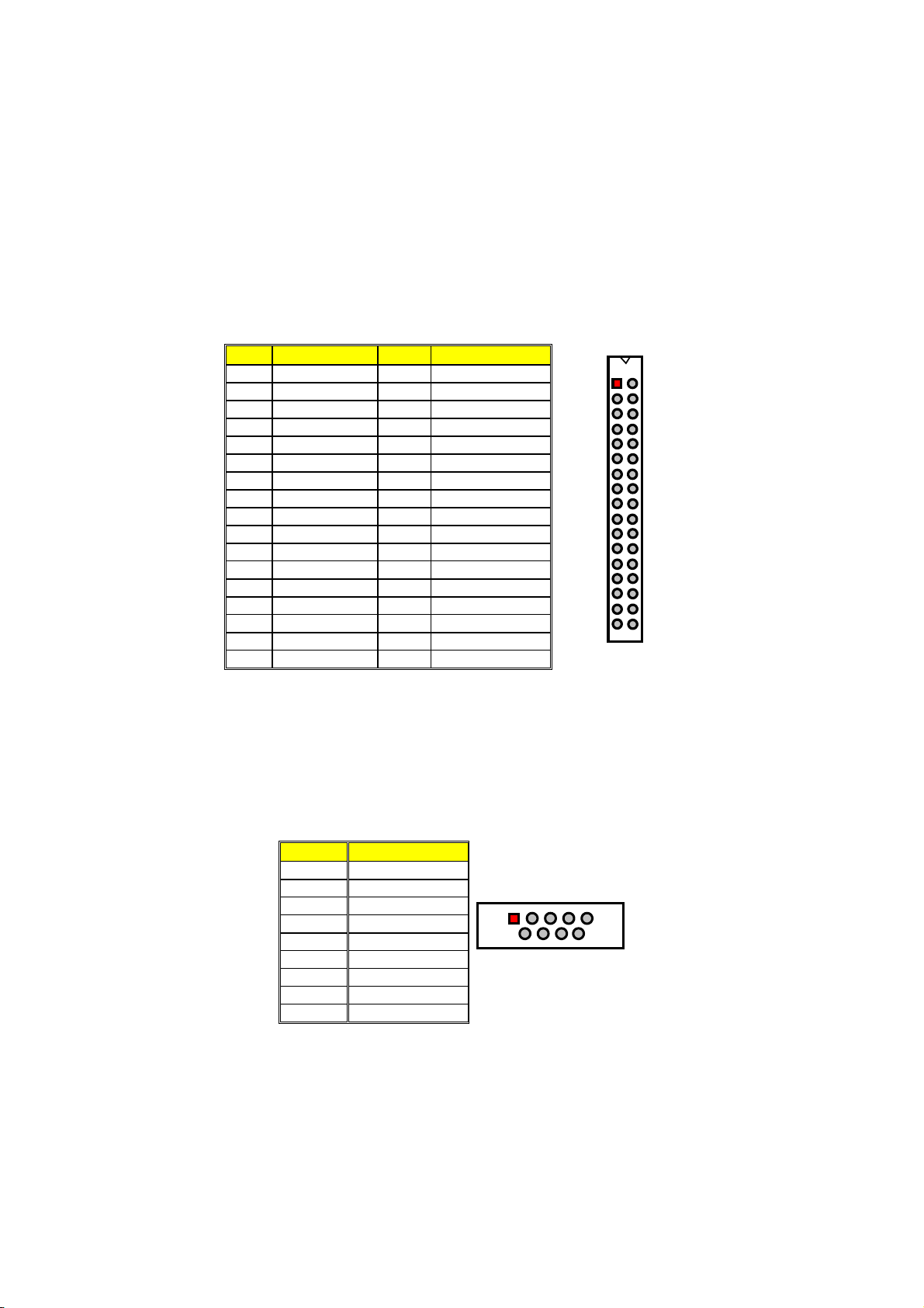
3.10 Floppy Disk Drive Connector
The HS-2603 uses a standard 34-pin header connector, CN15, for
floppy disk drive connection. A total of two FDD drives may be
connected to CN15 at any given time.
CN15: FDD Connector
PIN Description PIN Description
1 GND 2 RWC
3 GND 4 N/C
5 GND 6 DS1
7 GND 8 INDX
9 GND 10 M0A
11 GND 12 DSB
13 GND 14 DSA
15 GND 16 M0B
17 GND 18 DIRX
19 GND 20 STEPX
21
GND
22
23 GND 24 WE
25 GND 26 TRKX0
27 GND 28 WPX
29 N/C 30 RDATAX
31 GND 32 HDSEL
33 N/C 34 DSKCHG
WD
u
1
2
34
33
3.11 Serial Port Connectors
The HS-2603 offers four NS16C550 compatible UARTs with
Read/Receive 16byte FIFO serial ports. CN7 is the onboard serial
port supporting RS-422/485. Please refer to the following JP2 and
JP3 settings when enabling/disabling the RS-232 or RS-422/485
function.
CN13: COM1 Connector (DB9)
PIN Description
16
1 DCD
2
RXD
3 TXD
4 DTR
5 GND
6 DSR
7 RTS
8 CTS
9 RI
DCD
RXD
16
DSR
RTS
TXD
CTS
DTR
GND
5
9
RI
Page 23
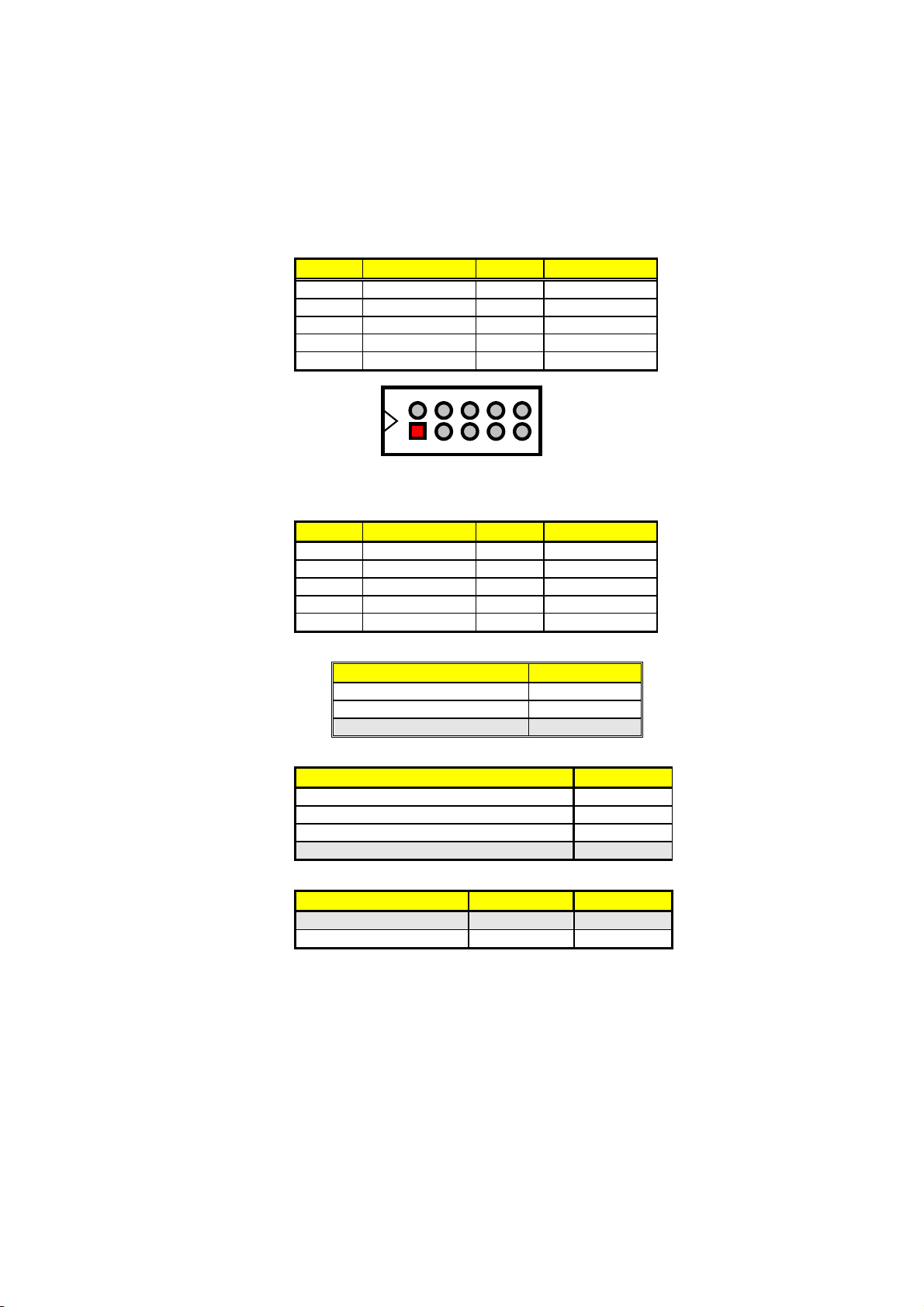
CN12, CN9 and CN11: COM2/COM3/COM4 Connectors (5x2
Header)
PIN Description PIN Description
1 DCD 2 DSR
3 RXD 4 RTX
5 TXD 6 CTX
7 DTR 8 RI
9
GND
246810
13579
CN7, CN9, CN11and CN12
10
N/C
CN7: RS-422/485 Connector (5x2 Header)
PIN Description PIN Description
1 TX- 2 TX+
3 RX+ 4 RX-
5 GND 6 RTS-
7
9 CTS- 10 N/C
JP2: RS-422/485 Receiver Enabled/Disabled Select
RTS+
8
Options Settings
Always Enable Short 1-2
Enable by “-RTS” signal Short 3-4
Always Disabled (default) * OPEN
JP3: RS-422/485 Transceiver Enabled/Disabled Select
Options Settings
Always Enable Short 1-2
Enable by “-RTS” signal
Enable by writing the REG:2 EFH BIT0=1 Short 5-6
Always Disabled (default) * OPEN
JP6, JP8: RS-232 or RS-422/485 Selection
Serial Port Setting JP6 JP8
* RS-232 (default) Short 1-3, 2-4 Short 1-3, 2-4
RS-422/485 Short 3-5, 4-6 Short 3-5, 4-6
CTS+
Short 3-4
17
Page 24
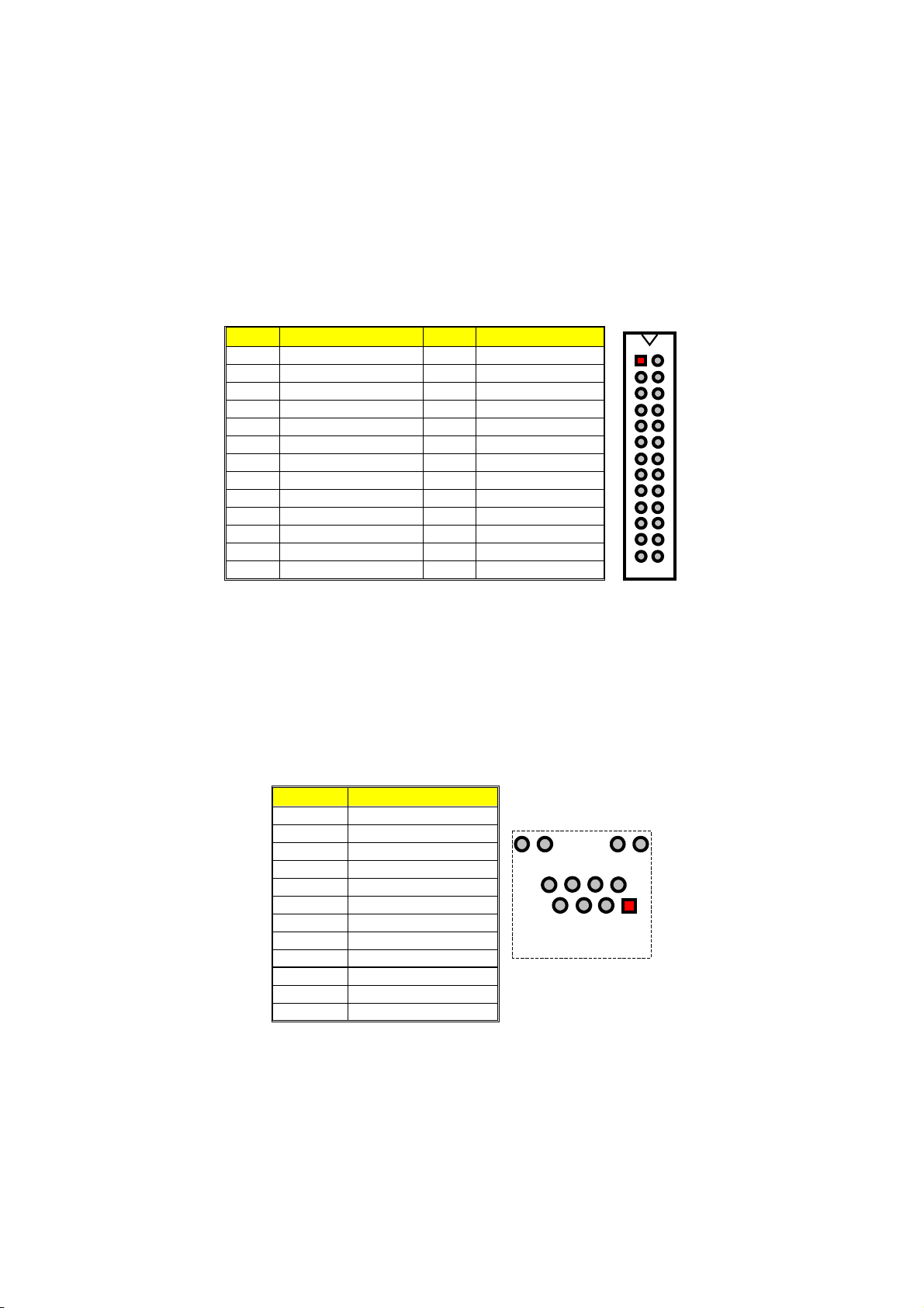
3.12 Parallel Connector
CN17 is a standard 26-pin flat cable connector designed to
accommodate parallel port connection onboard the HS-2603.
CN17: Parallel Connector
PIN Description PIN Description
1 STBX 2 D0
3 D1 4 D2
5 D3 6 D4
7 D5 8 D6
9
11 Busy 12 Paper Empty
13 Printer Select 14 Auto Form Feed
15 ERROR# 16 Initialize
17 Printer Select LN# 18 GND
19 GND 20 GND
21 GND 22 GND
23 GND 24 GND
25 GND 26 N/C
D7
10
Acknowledge
12
2625
3.13 Ethernet Connector
The Fast Ethernet controller provides with 32-bit performance, PCI bus
master capability, and full compliance with IEEE 802.3 10/100Based-T
specifications. For 10/100 Based operations, please connect the
network connection by plugging one end of the cable into the RJ-45 of
the CN4 connector. Please refer to the following detail of pin
information.
CN4: RJ-45 and LAN LED Connector
PIN Description
1
2 TX-
3 RX+
4 No Use
5 No Use
6 RX-
7 No Use
8 No Use
9 LNK LED
10 3.3V
11 ACT LED
12 3.3V
TX+
9101112
8
7
2
1
18
Page 25
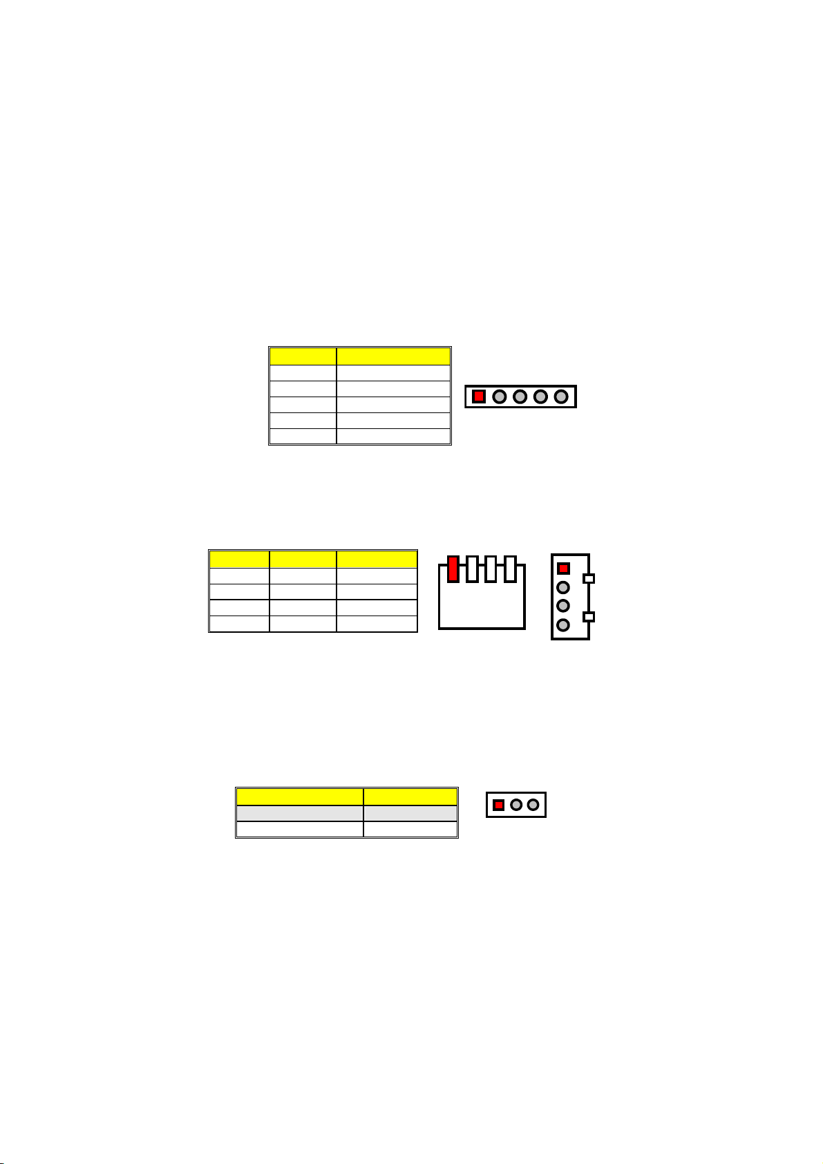
Aside from the RJ-45 provision onboard the HS-2603, the board also
features an LED indicator that displays the LINK and active status of
the LAN connection.
3.14 IrDA Connector
JP10 is a 5-pin internal IR communication connector for connection of
an IrDA device.
JP10: IrDA Connector
PIN Description
1 +5V
2
3 IRRX
4 GND
5 IRTX
CIRRX
12345
3.15 USB Connector
The HS-2603 provides two 4-pin connectors for USB0 & USB1 port
connections at location JP12 and JP13.
JP12 and JP13: USB Connectors
PIN JP12 JP13
1 VCC VCC
2 2DATA- 1DATA-
3 2DATA+ 1DATA+
4 GND GND
1 23 4
JP12
JP13
1
4
3.16 CMOS Data Clear
The HS-2603 has a Clear CMOS jumper on JP11. The JP11 settings
below apply to the standard HS-2603 using a battery backed up CMOS
chip.
JP11: Clear CMOS
Options Settings
Normal (default) Short 1-2
Clear CMOS Short 2-3
IMPORTANT:
The default setting of JP11 is Short 2-3. Before you turn on
the power of your system, please set JP11 to Short 1-2 for
normal operation.
1 23
19
Page 26
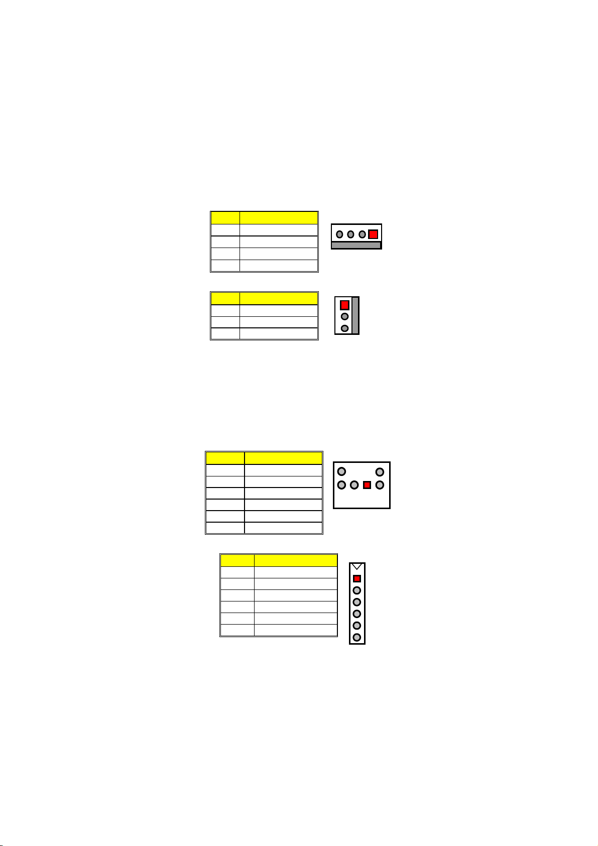
3.17 Power and Fan Connectors
HS-2603 provides one 4-pin power connector at CN14, and a fan
connector at FN1.
CN14: 4-pin Power Connector
PIN Description
1 VCC
2 GND
3 GND
4
FN1: FAN Connector
PIN Description
1 VCC 5V
2 GND
3
+12V
VCC 5V
4
+12V
1
3
GND
GND
1
VCC
3.18 Keyboard/Mouse Connectors
The HS-2603 offers two possibilities for keyboard connections. The
connections are via CN8 for an external PS/2 type keyboard/mouse or
via CN10 for an internal 6-pin cable converter to an AT keyboard. CN8
is a PS/2 6-pin Mini DIN connector that provides Mouse signals. With
CN8 alone, both the mouse and keyboard signals are supported.
CN8: 6-pin PS/2 Mini DIN Keyboard/Mouse Connector
PIN Description
1 KBDATRX
2 MSDATX
3 GND
4 VCC
5 KBCLKRX
6
CN10: 6-pin Keyboard/Mouse Connector
MSCLKX
PIN Description
1 KBCLKRX
2 KBDATRX
3 MSDATX
4 GND
5 VCC
6 MSCLKX
6
5
1234
1
2
3
4
5
6
20
Page 27
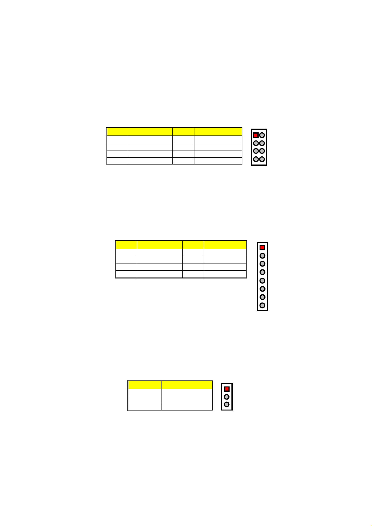
3.19 Front Panel Signal Connector
The CN1 connector of HS-2603 allows users connection to an external
control button.
CN1: Front Panel Signal Connector
PIN Description PIN Description
1 Reset 2 GND
3
5 Speaker 6 VCC5V
7 HDD LED 8 330Ω Pull +5V
N/C
4
GND
1
7
2
8
3.20 Audio Connector
The HS-2603 has an onboard Cyrix® CX5530 audio interface. The
following tables list the pin assignments of the Line In and the MIC In /
Audio Out connectors. This Line Out (or Audio Out) port supports a
preamp function that allows user to connect either a passive set of
speakers or earphones.
JP14: Line In/Line Out/Mic In Connector
PIN Description PIN Description
1
3 LININL 4 GND
5 MIC IN 6 GND
7 AOUT_L 8 AOUT_R
LININR
2
GND
1
8
3.21 TV Out Function
The HS-2603TV is the board version that supports the TV Out function.
This TV Out supports both S-Video and Composite Video signals via
jumpers JP5 and JP4 respectively. Additionally, the TV Out is universal
in that it allows users to switch their TV systems between NTSC and
PAL from within the Integrated Peripherals Setup of the BIOS utility.
JP5: S-Video Output
PIN Description
1 LUM
2 CHROM
3 GND
1
2
3
21
Page 28
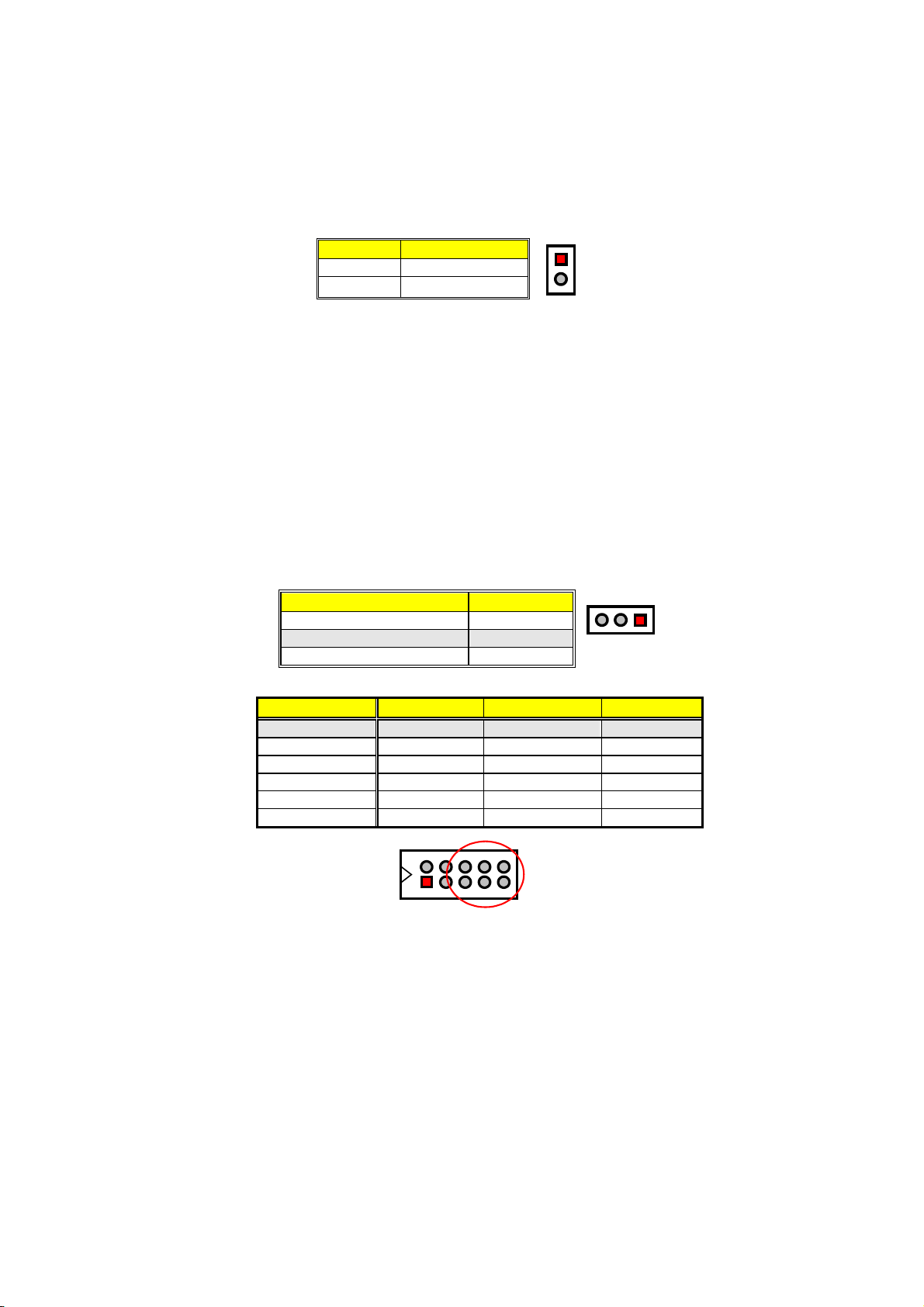
JP4: Composite Video Output
PIN Description
1 Composite
2 GND
3.22 Watchdog Timer
1
2
There are three access cycles of Watch-Dog Timer as
Enable, Refresh
and Disable are the three access cycles of Watchdog Timer. The
Enable cycle proceeds via READ PORT 443H whereas the Disable
cycle proceeds via READ PORT 045H. A continued Enable cycle after
a first Enable cycle means Refresh.
Once the Enable cycle is active, a Refresh cycle is requested before
the time-out period. This restarts counting of the WDT period. When
the time counting goes over the period preset of WDT, it will assume
that the program operation is abnormal. A System Reset signal to
re-start or a NMI cycle to the CPU transpires when such error happens.
Jumper JP7 is used to select the function of Watchdog Timer.
JP7: Watchdog Timer Active Type Setting
Options Settings
Active NMI Short 1-2
System Reset (default) Short 2-3
Disabled Watchdog Timer Open
JP9 (5-10): WDT Period Select
123
Period Pins 5-6 Pins 7-8 Pins 9-10
* 1 sec (default) Short Short Short
2 sec Open Short Short
10 sec Short Open Short
20 sec
110 sec Short Short Open
220 sec Open Short Open
Open Open Short
246810
13579
The Watchdog Timer is disabled after the system Power-On. It can be
enabled via an Enable cycle and reading the control port (443H), or via
a Refresh cycle and reading the control port (443H), or via a Disable
cycle and reading the disable control port (045H).
22
Page 29
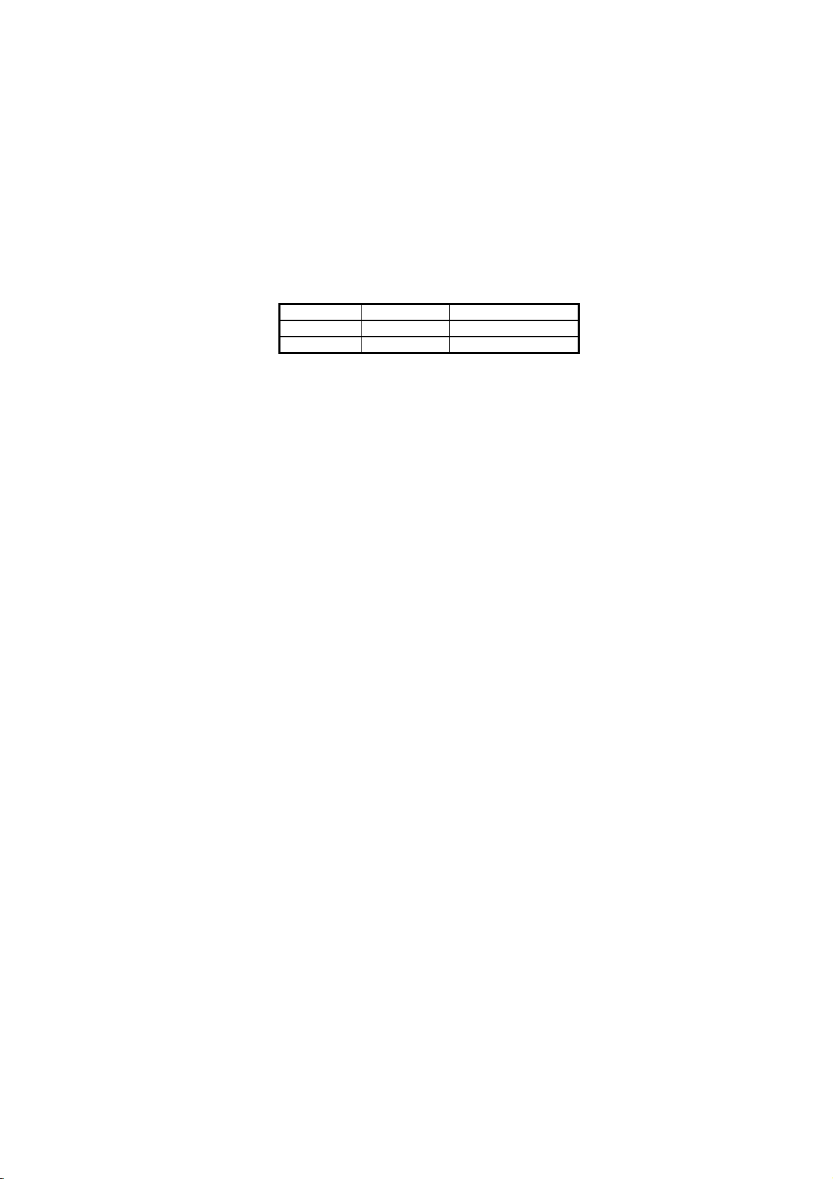
After an Enable cycle of WDT, user must immediately execute a
Refresh cycle to WDT before its period setting comes to an end every
1, 2, 10, 20, 110 or 220 seconds. If the Refresh cycle does not activate
before WDT period cycle, the onboard WDT architecture will issue a
Reset or NMI cycle to the system. There are three I/O ports that control
the Watchdog Timer.
443H I/O Read The Enable cycle
443H
I/O Read The Refresh cycle
045H I/O Read The Disable cycle
The following sample program shows how to Enable, Disable and
Refresh the Watchdog Timer:
WDT_EN_RF EQU 0433H
WDT_DIS EQU 0045H
WT_Enable PUSH AX ; keep AX DX
PUSH DX
MOV DX,WDT_EN_RF ; enable the WDT
IN AL,DX
POP DX ; get back AX, DX
POP AX
RET
WT_Refresh PUSH AX ; keep AX, DX
PUSH DX
MOV DX,WDT_ET_RF ; refresh the WDT
IN AL,DX
POP DX ; get back AX, DX
POP AX
RET
WT_DISABLE PUSH AX
PUSH DX
MOV DX,WDT_DIS ; disable the WDT
IN AL,DX
POP DX ; get back AX, DX
POP AX
RET
23
Page 30

3.23 CompactFlash Connector
The HS-2603 also offers an optional CompactFlash connector which
is IDE interface located at the solder side of the board (beneath the
SO-DIMM connector). The designated J1 connector, once soldered
with an adapter, can hold CompactFlash cards of various sizes.
Please turn off the power before inserting the CF card.
J1: CompactFlash Connector
PIN Description PIN Description
1 GND 2 DATA 3
3 DATA 4 4 DATA 5
5 DATA 7 6 DATA 7
7 HOC CS0# 8 GND
9 GND 10 GND
11 GND 12 GND
13
15 GND 16 GND
17 GND 18 PA 2
19 PA 1 20 PA 0
21 DATA 0 22 N/C
23
25 N/C 26 N/C
27 DATA 11 28 DATA 12
29 DATA 13 30 DATA 14
31 DATA 15 32 HDC CS1#
33 N/C 34 IOR
35 IOW 36 EWE0
37 IRQ 38 VCC (+5V)
39 N/C 40 N/C
41 Reset 42 IORDY
43 N/C 44 REQ 0
45 IDE LED 46 PDIAG
47 DATA 8 48 DATA 9
49
VCC (+5V)
DATA 1
DATA 10
14
24
50
GND
GND
GND
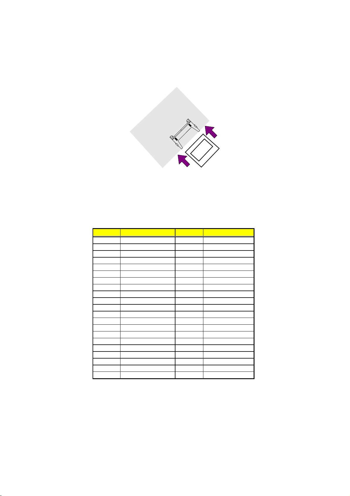
Inserting a CompactFlash card into the adapter is not a difficult task.
The socket and card are both keyed and there is only one direction for
the card to be completely inserted. Refer to the diagram on the
following page for the traditional way of inserting the card.
24
Page 31
r
de
w
ol
e
S
i
V
B
C
de
P
i
S
CompactFlash
M
T
e
d
i
/
S
n
n
r
o
a
p
a
p
a
a
e
J
J
R
u
n
i
A
F
e
e
d
C
u
a
q
i
M
r
b
a
F
E
C
3.24 Mini PCI Connector
HS-2603 supports a Mini PCI interface which is a very popular
notebook computer expansion interface for Modem, Video, LAN,
etc. The Mini PCI onboard HS-2603 is at location PC1 with pin
definitions listed on the table below.
PC1: Mini PCI Connector Pin Information
PIN Description PIN Description
1 INTB# 2 5V
3 3.3V 4 D#
5 RESERVED 6 RESERVED
7
GND
8
9 CLK 10 RST#
11 GND 12 3.3V
13 REQ# 14 GNT#
15 3.3V 16 GND
17
AD[31]
18
19 AD[29] 20 RESERVED
21 GND 22 AD[30]
23 AD[27] 24 3.3V
25 AD[25] 26 AD[28]
27 RESERVED 28 AD[26]
29 C/BE[3]# 30 AD[24]
31 AD[23] 32 IDSEL
33 GND 34 GND
35 AD[21] 36 AD[22]
37 AD[19] 38 AD[20]
39 GND 40 PAR
41 AD[17] 42 AD[18]
. . . More on next page . . .
N.C.
PME#
25
Page 32
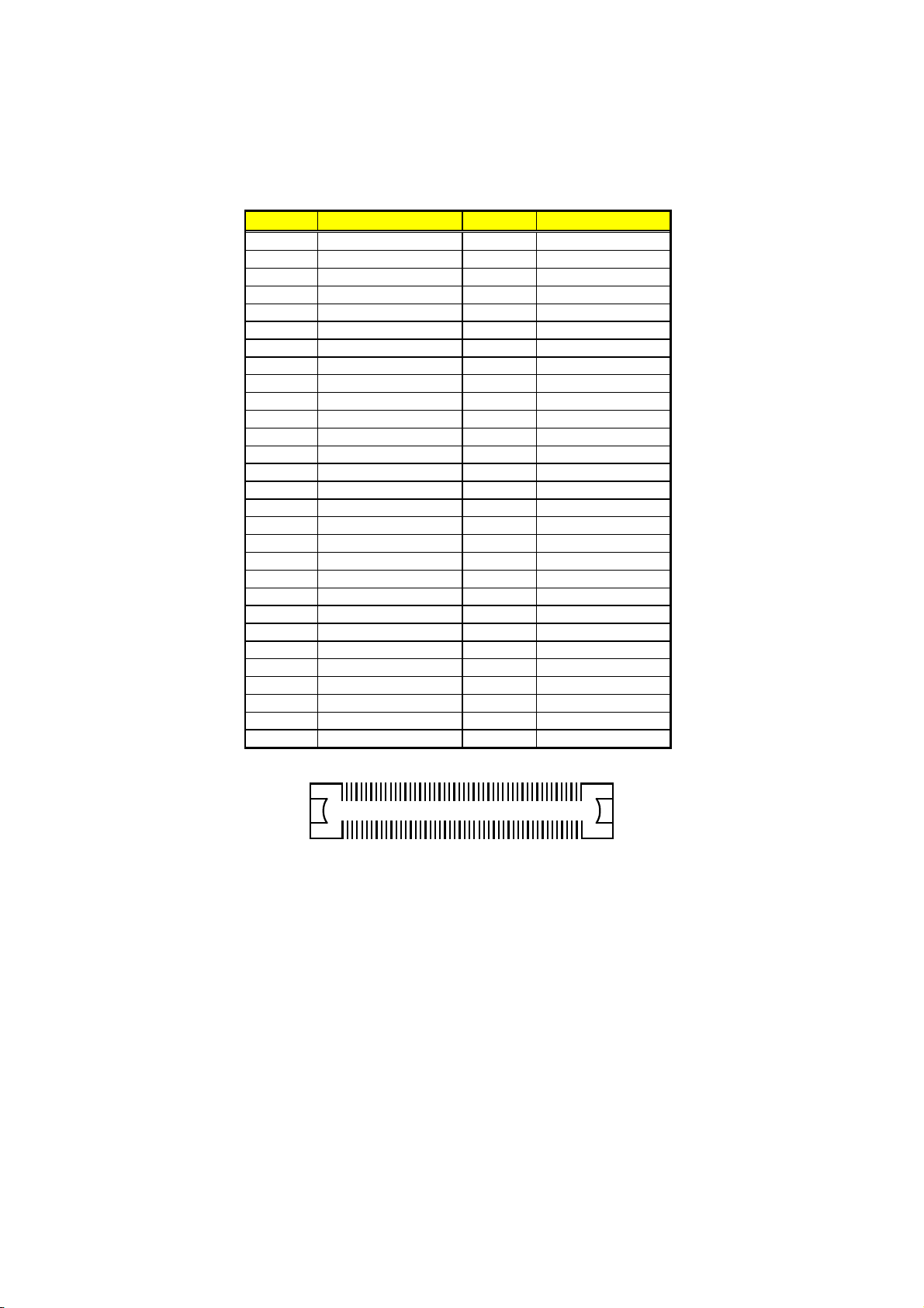
PIN Description PIN Description
43 C/BE[2]# 44 AD[16]
45 IRDY# 46 GND
47 3.3V 48 FRAME#
49 CLKRUN# 50 TRDY#
51 SERR# 52 STOP#
53 GND 54 3.3V
55 PERR# 56 DEVSEL#
57 C/BE[1]# 58 GND
59 AD[14] 60 AD[15]
61 GND 62 AD[13]
63 AD[12] 64 AD[11]
65
67 GND 68 AD[9]
69 AD[8] 70 C/BE[0]#
71 AD[7] 72 3.3V
73 3.3V 74 AD[6]
75
77 RESERVED 78 AD[2]
79 AD[3] 80 AD[0]
81 5V 82 RESERVED_WIP2
83 AD[1] 84 RESERVED_WIP2
85 GND 86 GND
87 AC_SYNC 88 M66EN
89 AC_SDATA_IN 90 AC_SDATA_OUT
91 AC_BIT_CLK 92 AC_CODEC_IDO#
93 AC_CODEC_ID1# 94 AC_RESET#
95 MOD_AUDIO_MON 96 RESERVED
97 AUDIO_GND 98 GND
99 SYS_AUDIO_OUT 100 SYS_AUDIO_IN
AD[10]
AD[5]
66
76
GND
AD[4]
26
2
199
Mini PCI Socket
pin orientation
100
Page 33
3.25 PC/104 Connectors
The PC/104 expansion bus offers provisions to connect all types of
PC/104 modules. With the PC/104 bus being known as the new
generation of industrial embedded 16bit PC standard bus, thousands
of PC/104 modules from multiple venders can be easily installed
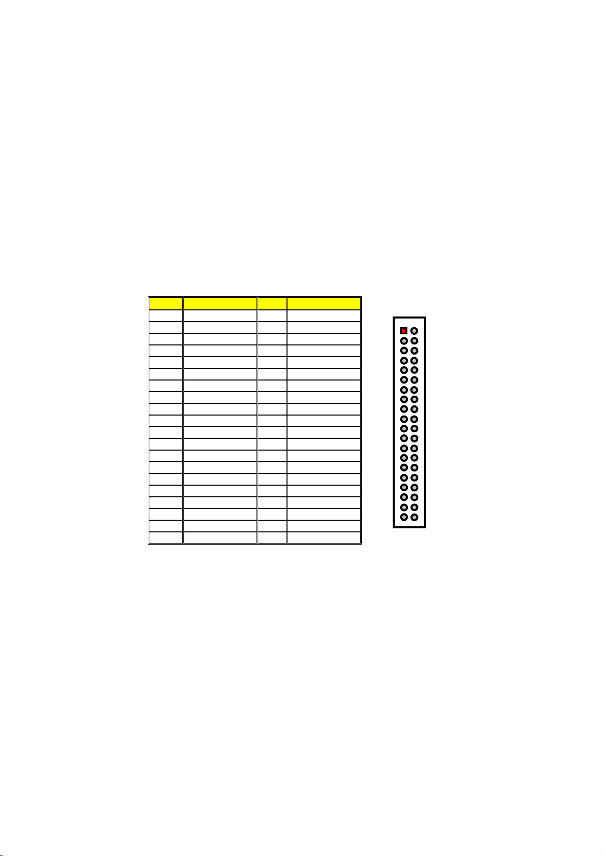
onboard. The detailed pin assignment of the PC/104 expansion bus
connectors CN10 and CN11 are listed on the following tables:
NOTE:
PIN Description PIN Description
10 DRQ0 30 MEMR*
11
12 DRQ5 32 SD8
13 DACK6* 33 SD9
14 DRQ6 34 SD10
15 DACK7* 35 SD11
16 DRQ7 36 SD12
17 +5V 37 SD13
18
19 GND 39 SD15
20 GND 40 N/C
The PC/104 connector allows direct plugging or stack-through
piling of PC/104 modules without requiring the PC/104 mounting
kit.
CN2: 40-pin PC/104 Expansion Slot
1 GND 21 GND
2 MEMCS16* 22 SBHE*
3 IOSC16* 23 LA23
4 IRQ10 24 LA22
5 IRQ11 25 LA21
6 IRQ12 26 LA20
7 IRQ15 27 LA19
8 IRQ14 28 LA18
9 DACK0* 29 LA17
DACK5*
MASTER*
31
38
MEMW*
SD14
121
20
40
27
Page 34
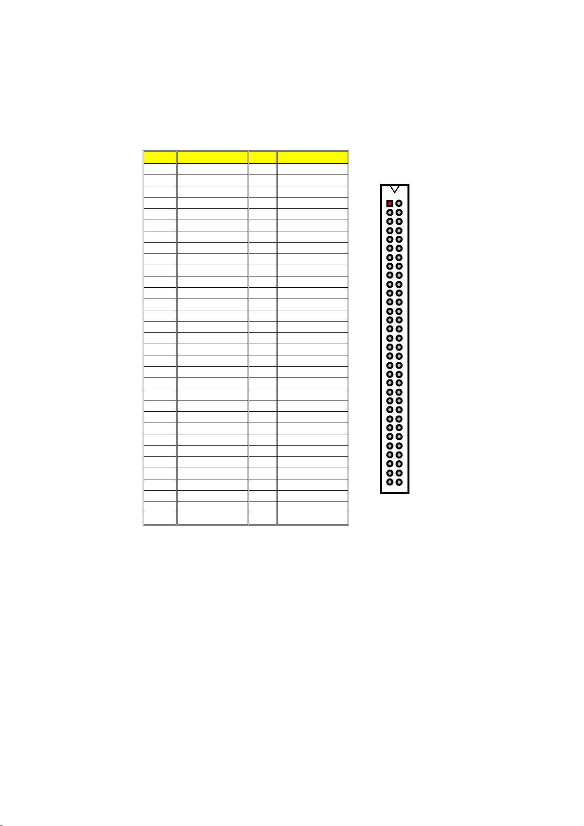
CN3: 64-pin PC/104 Expansion Slot
PIN Description PIN Description
1 IOCHECK* 33 GND
2 SD7 34 RESETDRV
3 SD6 35 +5V
4
SD5
36
5 SD4 37 -5V
6 SD3 38 DRQ2
7 SD2 39 -12V
8 SD1 40 NOW*
9 SD0 41 +12V
10 IOCHRDY 42 GND
11 AEN 43 SMEMW*
12 SA19 44 SMEMR*
13 SA18 45 IOW*
14 SA17 46 IOR*
15 SA16 47 DACK3*
16
SA15
48
17 SA14 49 DACK1*
18 SA13 50 DRQ1
19 SA12 51 REFRESH*
20 SA11 52 SYSCLK
21 SA10 53 IRQ7
22 SA9 54 IRQ6
23 SA8 55 IRQ5
24 SA7 56 IRQ4
25 SA6 57 IRQ3
26 SA5 58 DACK2*
27 SA4 59 TC
28
SA3
60
29 SA2 61 +5V
30 SA1 62 OSC
31 SA0 63 GND
32 GND 64 GND
IRQ9
DRQ3
BALE
133
6432
28
Page 35

Chapter 4
Award BIOS Setup
The HS-2603 uses Award PCI/ISA BIOS for the system configuration.
The Award BIOS setup program is designed to provide the maximum
flexibility in configuring the system by offering various options that
could be selected for end-user requirements. This chapter is written to
assist you in the proper usage of these features.
4.1 Starting Setup
The Award BIOS is immediately activated when you first power on the
computer. The BIOS reads the system information contained in the
CMOS and begins the process of checking out the system and
configuring it. When it finishes, the BIOS will seek an operating system
on one of the disks and then launch and turn control over to the
operating system.
While the BIOS is in control, the Setup program can be activated in one
of two ways:
1. By pressing <Del> immediately after switching the system
on, or
2. By pressing the <Del> key when the following message
appears briefly at the bottom of the screen during the POST
(Power On Self Test).
Press DEL to enter SETUP.
If the message disappears before you respond and you still wish to
enter Setup, restart the system to try again by turning it OFF then ON or
pressing the "RESET" button on the system case. You may also restart
by simultaneously pressing <Ctrl>, <Alt>, and <Delete> keys. If you do
not press the keys at the correct time and the system does not boot, an
error message will be displayed and you will again be asked to...
PRESS F1 TO CONTINUE, DEL TO ENTER SETUP
29
Page 36

4.2 Using Setup
In general, you use the arrow keys to highlight items, press <Enter> to
select, use the <PageUp> and <PageDown> keys to change entries,
press <F1> for help and press <Esc> to quit. The following table
provides more detail about how to navigate in the Setup program using
the keyboard.
Up arrow Move to previous item
Down arrow Move to next item
Left arrow Move to the item in the left hand
Right arrow Move to the item in the right hand
Esc key Main Menu -- Quit and not save changes into CMOS
Status Page Setup Menu and Option Page Setup Menu -Exit current page and return to Main Menu
PgUp key
PgDn key Decrease the numeric value or make changes
+ key Increase the numeric value or make changes
- key Decrease the numeric value or make changes
F1 key General help, only for Status Page Setup Menu and Option
(Shift)F2 key Change color from total 16 colors. F2 to select color
F3 key Calendar, only for Status Page Setup Menu
F4 key
F5 key Restore the previous CMOS value from CMOS, only for
F6 key Load the default CMOS value from BIOS default table, only
F7 key Load the default
F8 key Reserved
F9 key Reserved
F10 key Save all the CMOS changes, only for Main Menu
Increase the numeric value or make changes
Page Setup Menu
forward, (Shift) F2 to select color backward
Reserved
Option Page Setup Menu
for Option Page Setup Menu
4.2.1 Getting Help
Press F1 to pop up a small help window that describes the appropriate
keys to use and the possible selections for the highlighted item. To exit
the Help Window press <Esc> or the F1 key again.
30
Page 37
4.3 Main Menu
Once you enter the Award BIOS CMOS Setup Utility, the Main Menu
will appear on the screen. The Main Menu allows you to select from
several setup functions and two exit choices. Use the arrow keys to
select among the items and press <Enter> to enter the sub-menu.
ROM PCI/ISA BIOS (2A434D2B)
CMOS SETUP UTILITY
AWARD SOFTWARE, INC.
STANDARD CMOS SETUP
BIOS FEATURES SETUP
CHIPSET FEATURES SETUP
POWER MANGEMENT SETUP
PNP/PCI CONFIGURATION
LOAD BIOS DEFAULTS
LOAD SETUP DEFAULTS
Esc:Quit
F10:Save & Exit
INTEGRATED PERIPHERALS
SUPERVISOR PASSWORD
USER PASSWORD
IDE HDD AUTO DETECTION
SAVE & EXIT SETUP
EXIT WITHOUT SAVING
:
(Shift)F2:Change Color
Select Item
NOTE:
A brief description of the highlighted choice appears at the bottom
of the screen.
Standard CMOS Setup
This setup page includes all the items in a standard, AT-compatible BIOS.
BIOS Features Setup
This setup page includes all the items of Award special enhanced features.
Chipset Features Setup
This setup page includes all the items of chipset special features.
Power Management Setup
This entry only appears if your system supports Power Management,
“Green PC”, standards.
PNP/PCI Configuration Setup
This entry appears if your system supports PNP/PCI.
Load BIOS Defaults
The BIOS defaults have been set by the manufacturer and represent
settings that provide the minimum requirements for your system to operate.
31
Page 38

Load Setup Defaults
The chipset defaults are settings that provide for maximum system
performance. While Award has designed the custom BIOS to maximize
performance, the manufacturer has the right to change these defaults to
meet their needs.
Integrated Peripherals
This section page includes all the items of IDE hard drive and Programmed
Input / Output features.
Set Supervisor / User Password
Change, set, or disable password. It allows you to limit access to the system
and Setup, or just to Setup.
IDE HDD Auto Detection
Automatically detect and configure hard disk parameters. The Award BIOS
includes this ability in the event you are uncertain of your hard disk’s
parameters.
Save & Exit Setup
Save CMOS value changes to CMOS and exit setup.
Exit Without Saving
Abandon all CMOS value changes and exit setup.
32
Page 39
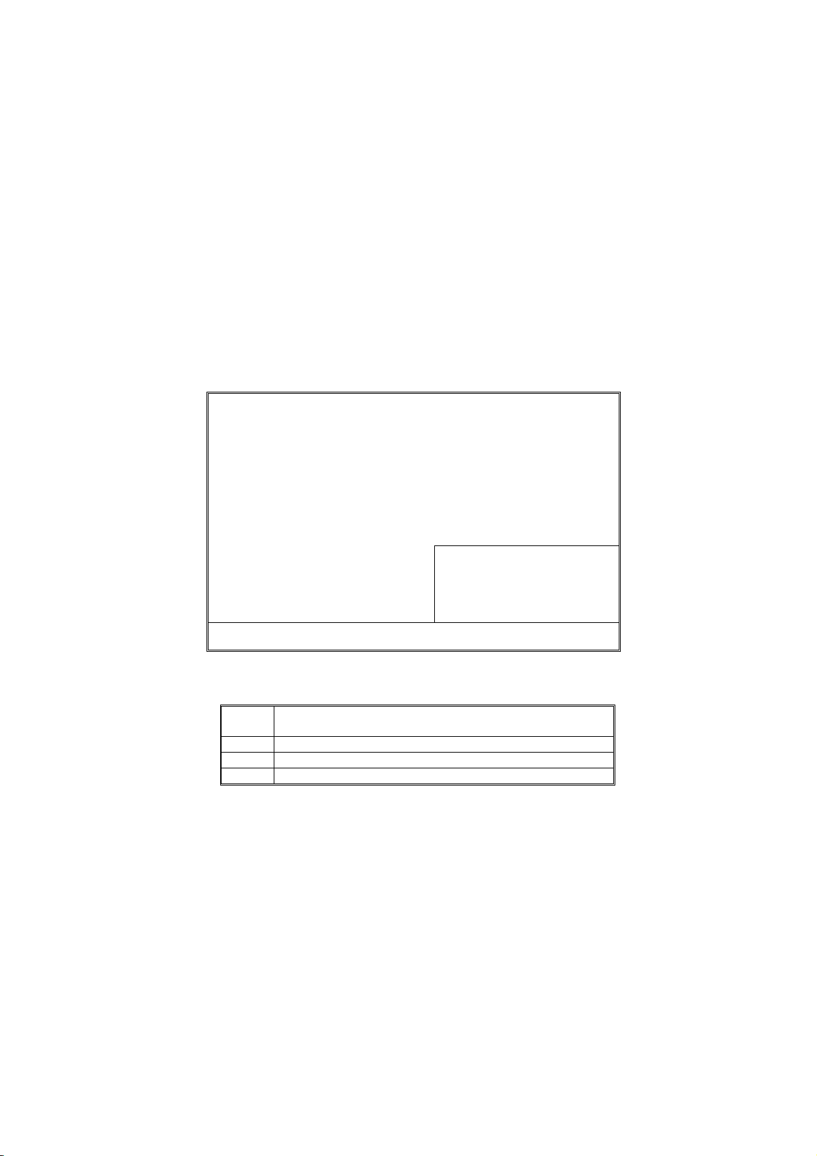
4.4 Standard CMOS Setup
0 0 0 0 0
0 0 0 0 0
0 0 0 0 0
0 0 0 0 0
The Standard Setup is used for the basic hardware system
configuration. The main function is for Data/Time and Floppy/Hard Disk
Drive settings. Please refer to the following screen for the setup. When
the IDE hard disk drive you are using is larger than 528MB, you must
set the HDD mode to
BIOS SETUP to install the HDD correctly.
Data (mm:dd:yy) : Fri, Dec 19 1998
Time (hh:mm:ss) : 00:00:00
TYPE SIZE CYLS HEAD PRECOMP LANDZ SECTOR MODE
Primary Master : 0 0
Primary Slave
Secondary Master : 47 0
Secondary Slave : 47 0
Drive A : 1.44M , 3.5 in.
Drive B : None
Base Memory : 640K
Video : EGA/VGA Extended Memory : 15360K
Other Memory : 384K
Halt On : All, But Keyboard Total Memory : 16384K
ESC : Quit
F1 : Help
:
0 0
mode. Please use the IDE Setup Utility in
LBA
ROM PCI/ISA BIOS (2A434D2B)
STANDARD CMOS SETUP
AWARD SOFTWARE, INC.
: Select Item
PU/PD/ + / - : Modify
(Shift) F2: Change Color
AUTO
AUTO
AUTO
AUTO
Date:
The date format is <day>, <date> <month> <year>. Press <F3> to
show the calendar.
day The day, from Sun to Sat, determined by the BIOS and is
display-only
date The date, from 1 to 31 (or the maximum allowed in the month)
month The month, Jan through Dec.
year The year, from 1900 through 2099
Time:
The time format is <hour> <minute> <second>. The time is
calculated based on the 24-hour military-time clock. For example,
1 p.m. is 13:00:00.
33
Page 40
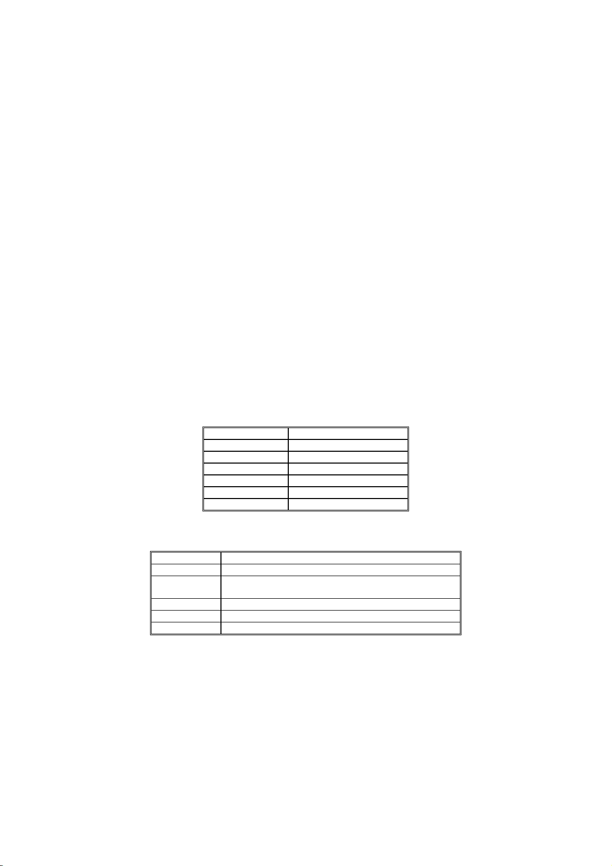
Primary Master/Slave & Secondary Master/Slave Drives:
The categories identify the types of 4 channels that have been
installed in the computer. There are 45 predefined types with 4
user-definable types for Enhanced IDE BIOS. Type 1 to Type 45
are predefined. Type user is user-definable.
Press PgUp or PgDn to select a numbered hard disk type or type
the number and press <Enter>. Note that the specifications of
your drive must match with the drive table. The hard disk will not
work properly if you enter improper information for this category. If
your hard disk drive type is not matched or listed, you can use
Type “User” to define your own drive type manually.
If you select Type “User”, you will need to know the information
listed below. Enter the information directly from the keyboard and
press <Enter>. This information should be included in the
documentation from your hard disk vendor or the system
manufacturer.
If the controller of HDD interface is ESDI, the selection shall be
“Type 1”.
If the controller of HDD interface is SCSI, the selection shall be
“None”.
If you select Type ”Auto”, BIOS will Auto-Detect the HDD &
CD-ROM Drive at the POST stage and showing the IDE for HDD
& CD-ROM Drive.
If a hard disk has not been installed select NONE and press
<Enter>.
TYPE drive type
CYLS. number of cylinders
HEADS
PRECOMP write precompensation
LANDZONE landing zone
SECTORS number of sectors
MODE mode type
number of heads
Drive A / Drive B:
The category identifies the types of floppy disk drive A or drive B
that have been installed in the computer.
None No floppy drive installed
360K, 5.25 in 5-1/4 inch PC-type standard drive; 360 kilobyte capacity
1.2M, 5.25 in 5-1/4 inch AT-type high-density drive; 1.2 megabyte
capacity
720K, 3.5 in 3-1/2 inch double-sided drive; 720 kilobyte capacity
1.44M, 3.5 in
2.88M, 3.5 in 3-1/2 inch double-sided drive; 2.88 megabyte capacity
3-1/2 inch double-sided drive; 1.44 megabyte capacity
34
Page 41
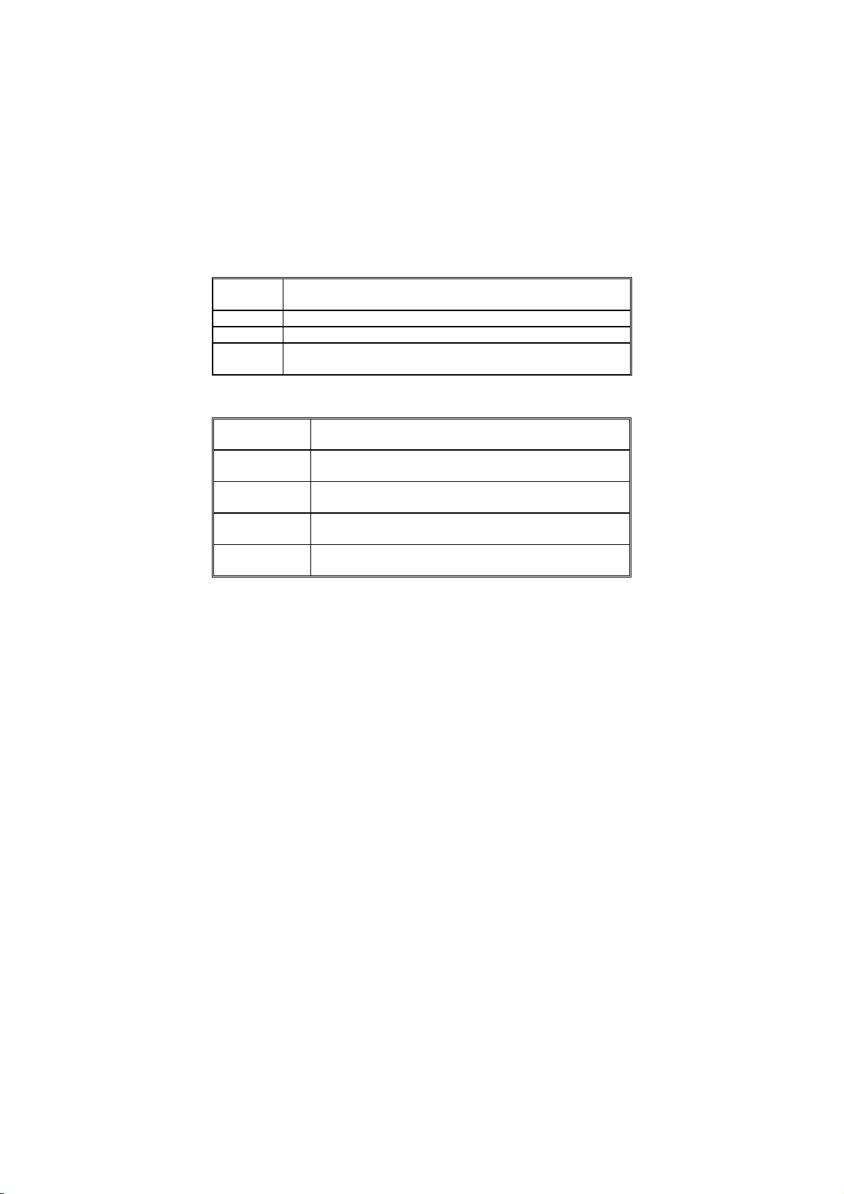
Video:
The category selects the type of video adapter used for the
primary system monitor. Although secondary monitors are
supported, you do not have to select the type in Setup.
EGA/VGA Enhanced Graphics Adapter/Video Graphics Array. For EGA,
VGA, SEGA, SVGA or PGA monitor adapters.
CGA 40 Color Graphics Adapter, power up in 40 column mode
CGA 80 Color Graphics Adapter, power up in 80 column mode
MONO Monochrome adapter, includes high resolution monochrome
adapters
Halt On: The category determines whether the computer will stop if an
error is detected during power up.
No errors The system boot will not be stopped for any error that
may be detected.
All errors Whenever the BIOS detects a non-fatal error the system
will be stopped and you will be prompted.
All,
But Keyboard
All, But
Diskette
All, But
Disk/Key
The system boot will not stop for a keyboard error; it will
stop for all other errors.
The system boot will not stop for a disk error; it will stop
for all other errors.
The system boot will not stop for a keyboard or disk
error; it will stop for all other errors.
Memory:
The category is display-only that is determined by POST (Power
On Self Test) of the BIOS.
Base Memory: The POST will determine the amount of base
Extended Memory: The BIOS determines how much extended
Total Memory: This refers to the memory located in the 640K
(or conventional) memory installed in the
system. The value of the base memory is
typically 512K for systems with 512K memory
installed on the motherboard, or 640K for
systems with 640K or more memory installed
on the motherboard.
memory is present during the POST. This is
the amount of memory located above 1MB
in the CPU's memory address map.
to 1024K address space. This is memory that
can be used for different applications. DOS
uses this area to load device drivers in an effort
to keep as much base memory free for
application programs. The BIOS is the most
frequent user of this RAM area since this is
where it shadows RAM
35
Page 42
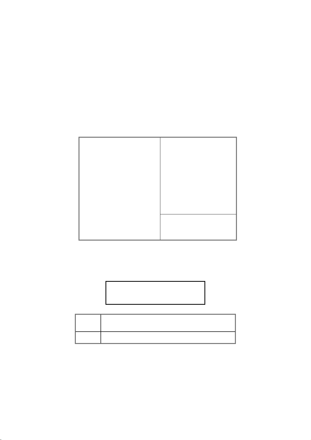
4.5 BIOS Features Setup
This section allows you to configure your system for the basic
operation. You have the opportunity to select the system’s default
speed, boot-up sequence, keyboard operation, shadowing and
security.
ROM PCI/ISA BIOS (2A434D2B)
BIOS FEATURES SETUP
AWARD SOFTWARE, INC.
Virus Warning : Disabled Video BIOS Shadow : Disabled
CPU Internal Cache : Enabled C8000-CBFFF Shadow : Disabled
CC000-CFFFF Shadow : Disabled
Quick Power On Self Test : Disabled D0000-D3FFF Shadow : Disabled
Boot Sequence : A,C,SCSI D4000-D7FFF Shadow : Disabled
Swap Floppy Drive : Disabled D8000-DBFFF Shadow : Disabled
Boot Up Floppy Seek : Enabled DC000-DFFFF Shadow : Disabled
Boot Up NumLock Status : On Cyrix 6x86/MII CPUID : Enabled
Boot Up System Speed : Low
Gate A20 Option : Normal
Memory Parity Check : Disabled
Typematic Rate Setting : Disabled
Typematic Rate (Chars/Sec) : 6
Typematic Delay (Msec) : 250
Security Option : Setup
PCI/VGA Palette Snoop : Disabled ESC : Quit
Assign IRQ for VGA : Disabled F1 : Help PU/PD/+/-: Modify
OS Select For DRAM > 64MB : Non-OS2 F5 : Old Values (Shift) F2 : Color
Report No FDD For WIN 95 : Yes F6 : Load BIOS Defaults
F7 : Load Setup Defaults
: Select Item
Virus Warning:
When this item is enabled, the Award BIOS will monitor the boot
sector and partition table of the hard disk drive for any attempt at
modification. If an attempt is made, the BIOS will halt the system
and the following error message will appear. Afterwards, if
necessary, you will be able to run an anti-virus program to locate
and remove the problem before any damage is done.
! WARNING !
Disk boot sector is to be modified
Type "Y" to accept write or "N" to abort write
Award Software, Inc.
Enabled Activates automatically when the system boots up causing a
warning message to appear when anything attempts to access
the boot sector or hard disk partition table.
Disabled No warning message will appear when anything attempts to
access the boot sector or hard disk partition table.
36
Page 43
NOTE:
Many disk diagnostic programs that attempt to access the boot
sector table can cause the above warning message. If you will be
running such a program, we recommend that you first disable
Virus Protection beforehand.
CPU Internal Cache:
These two categories speed up memory access. However, it
depends on CPU/chipset design. The default value is en able.
Enabled Enable cache
Disabled Disable cache
Quick Power On Self Test:
Boot Sequence:
This category speeds up Power On Self Test (POST) after you
power up the computer. If it is set to Enable, BIOS will shorten or
skip some check items during POST.
Enabled
Disabled Normal POST
This category determines which drive to search first for the disk
operating system (i.e., DOS). The available options are:
Enable quick POST
A, C, SCSI SCSI, C, A
C, S, SCSI C only
C, CD-ROM, A LS, C
CD-ROM, C, A Zip100, C
D, A, SCSI USB-FDD, C
E, A, SCSI USB-Zip, C
F, A, SCSI USB-CD, C
SCSI, A, C USB-HDD, C
Boot Up Floppy Seek:
During POST, BIOS will determine if the floppy disk drive installed
is 40 or 80 tracks. 360K type is 40 tracks while 760K, 1.2M and
1.44M are all 80 tracks.
Enabled BIOS searches for floppy disk drive to determine if it is 40 or
80 tracks. Note that BIOS cannot tell from 720K, 1.2M or
1.44M drive type as they are all 80 tracks.
Disabled
BIOS will not search for the type of floppy disk drive by track
number. Note that there will not be any warning message if
the drive installed is 360K.
Boot Up NumLock Status:
This allows you to determine the default state of the numeric
keypad. By default, the system boots up with NumLock on.
On Keypad is number keys
Off Keypad is arrow keys
37
Page 44
Boot Up System Speed:
Selects the default system speed -- the normal operating speed at
power up.
Gate A20 Option:
This entry allows you to select how the gate A20 is handled. The
gate A20 is a device used to address memory above 1 Mbytes.
Initially, the gate A20 was handled via a pin on the keyboard.
Today, while keyboards still provide this support, it is more
common, and much faster, for the system chipset to provide
support for gate A20.
High Set the speed to high
Low Set the speed to low
Normal keyboard
Fast
chipset
Memory Parity Check:
Typematic Delay (Msec):
Select Enabled if the DRAM chips in your system support parity.
Typematic Rate (Chars/Sec):
When the typematic rate is enabled, this selection allows you
select the rate at which the keys are accelerated.
6 6 characters per second
8 8 characters per second
10 10 characters per second
12 12 characters per second
15 15 characters per second
20 20 characters per second
24 24 characters per second
30 30 characters per second
When the typematic rate is enabled, this selection allows you to
select the delay between when the key was first depressed and
when the acceleration begins.
250 250 msec
500 500 msec
750 750 msec
1000 1000 msec
Security Option:
This category allows you to limit access to the system and Setup,
or just to Setup.
System The system will not boot and access to Setup will be denied if
the correct password is not entered at the prompt.
Setup The system will boot, but access to Setup will be denied if the
correct password is not entered at the prompt.
38
Page 45
NOTE:
To disable security, select PASSWORD SETTING at Main Menu
and then you will be asked to enter password. Do not type anything
and just press <Enter>, it will disable security. Once the security is
disabled, the system will boot and you can enter Setup freely.
PCI/VGA Palette Snoop:
It determines whether the MPEG ISA/VESA VGA Cards can work
with PCI/VGA or not.
Enabled When PCI/VGA working with MPEG ISA/VESA VGA Card
Disabled When PCI/VGA not working with MPEG ISA/VESA VGA Card
Assign IRQ for VGA:
OS Select For DRAM > 64MB:
Video BIOS Shadow:
C8000 - CBFFF Shadow/D0000 - DFFFF Shadow:
Cyrix 6x86/MII CPUID:
This option turns on or off the IRQ assignment of the VGA port.
This item allows you to access the memory that over 64MB in
OS/2. The available choices are Non-OS2, OS2.
Report No FDD For WIN 95:
Whether report no FDD for Win 95 or not. The available choices
are Yes, No.
Determines whether video BIOS will be copied to RAM. However,
it is optional depending on chipset design. Video Shadow will
increase the video speed.
Enabled
Disabled Video shadow is disabled
These categories determine whether option ROMs will be copied
to RAM. An example of such option ROM would be support of
on-board SCSI.
Enabled Optional shadow is enabled
Disabled
This item allows you to view the CPU ID of your Cyrix chip during
the boot up process of your computer. The available choices are
Enabled and Disabled.
Video shadow is enabled
Optional shadow is disabled
39
Page 46

4.6 Chipset Features Setup
This section allows you to configure the system based on the specific
features of the installed chipset. This chipset manages bus speeds and
the access to the system memory resources, such as DRAM and the
external cache. It also coordinates the communications between the
conventional ISA and PCI buses. It must be stated that these items
should never be altered. The default settings have been chosen
because they provide the best operating conditions for your system.
You might consider and make any changes only if you discover that the
data has been lost while using your system.
ROM PCI/ISA BIOS (2A434D2B)
CHIPSET FEATURES SETUP
AWARD SOFTWARE, INC.
SDRAM CAS latency Time : Auto
SDRAM Clock Ratio Div By : 3
16-bit I/O Recovery (CLK) : 2
8-bit I/O Recovery (CLK) : 3
USB Controller : Enabled
USB Legacy Support : Enabled
Video Memory Size : 4M
Flat Panel Status : Enabled
Flat Panel Resolution : 600x800
ESC : Quit
F1 : Help PU/PD/+/-: Modify
F5 : Old Values (Shift) F2 : Color
F6 : Load BIOS Defaults
F7 : Load Setup Defaults
: Select Item
SDRAM CAS latency Time:
You can select CAS latency time in HCLKs of 2/2 or 3/3. The
system board designer should set the values in this field,
depending on the DRAM installed. Do not change the values in
this field unless you change specifications of the installed DRAM
or the installed CPU. The available choices are 2, 3.
16-bit I/O Recovery (CLK) :
The I/O recovery mechanism adds bus clock cycles between
PCI-originated I/O cycles to the ISA bus. This delay takes place
because the PCI bus is so much faster than the ISA bus. The
available choices range from 1 to 16 CPU clocks.
40
Page 47

8-bit I/O Recovery (CLK):
The I/O recovery mechanism adds bus clock cycles between
PCI-originated I/O cycles to the ISA bus. This delay takes place
because the PCI bus is so much faster than the ISA bus.
This item allows you to determine the recovery time allowed for 8
bit I/O. The available choices range from 1 to 16 CPU clocks.
USB Controller:
USB Legacy Support:
Flat Panel Status:
Flat Panel Resolution:
Select Enabled if your system contains a Universal Serial Bus
(USB) controller and you have a USB keyboard. The available
choices are Enabled, and Disabled.
With USB devices installed on your system, enabling the USB
legacy support allows the user to operate the USB devices under
DOS mode. The available choices are Enabled and Disabled.
Video Memory Size:
Select the Video memory size. The available choices are 1.25M,
1.5M, and 2.125M.
This item lets you turn on/off the flat panel connection of your
system. If a flat panel is connected to your system and you failed
to enable this item, your flat panel will not work. The available
choices are Enabled and Disabled.
Once the flat panel status is set from the previous item, user may
now select the flat panel resolution, from this item, that he intends
to display. The available choices are 640x480, 800x600, and
1024x768.
41
Page 48
4.7 Power Management Setup
The Power Management Setup allows user to configure the system for
saving energy in a most effective way while operating in a manner
consistent with his own style of computer use.
ROM PCI/ISA BIOS (2A434D2B)
POWER MANAGEMENT SETUP
AWARD SOFTWARE, INC.
Power Management : Disabled IRQ1 (KeyBoard) : ON
* * PM Timers * *
Doze Mode : Disabled IRQ4 (COM1) : OFF
Standby Mode : Disabled IRQ5 (LPT2) : OFF
HDD Power Down : Disabled IRQ6 (Floppy Disk) : OFF
MODEN Use IRQ : NA IRQ7 (LPT1) : OFF
IRQ9 (IRQ2 Redir) : OFF
Throttle Duty Cycle : 33.3% IRQ10 (Reserved) : OFF
IRQ11 (Reserved) : OFF
RING POWER ON Controller : Disabled IRQ12 (PS/2 Mouse) :
Net POWER ON Controller : Disabled IRQ13 (Coprocessor) : OFF
Wake-Up System By PME : Disabled IRQ14 (Hard Disk) : OFF
RTC Alarm Function : IRQ15 (Reserved) : OFF
RTCOn by Time (hh:mm) : 7:0
ESC : Quit
F1 : Help PU/PD/+/-: Modify
F5 : Old Values (Shift) F2 : Color
F6 : Load BIOS Defaults
F7 : Load Setup Defaults
IRQ3 (COM2) : OFF
OFF
: Select Item
Power Management:
This category allows you to select the type (or degree) of power
saving and is directly related to the following modes:
Doze Mode
Standby Mode
Suspend Mode
HDD Power Down
There are four selections for Power Management, three of which have
fixed mode settings.
Disable (default) No power management. Disables all four modes
Min. Power Saving Minimum power management. Doze Mode = 1 hr.
Standby Mode = 1 hr., Suspend Mode = 1 hr., and
HDD Power Down = 15 min.
Max. Power
Saving
Maximum power management -- ONLY AVAILABLE
FOR SL CPU’S. Doze Mode = 1 min., Standby Mode
= 1 min., Suspend Mode = 1 min., and HDD Power
Down = 1 min.
User Defined Allows you to set each mode individually. When not
disabled, each range is from 1 min. to 1 hr. except for
HDD Power Down that ranges from 1 min. to 15 min.
and disable.
42
Page 49
PM Control by APM:
When enabled, an Advanced Power Management device will be
activated to enhance the Max. Power Saving mode and stop the
CPU internal clock. If the Max. Power Saving is not enabled, this
will be preset to No.
Video Off Method:
MODEM Use IRQ:
This determines the manner in which the monitor is blanked.
V/H SYNC+Blank
Blank Screen
DPMS
Video Off After:
When enabled, this feature allows the VGA adapter to operate in a
power saving mode.
N/A
Suspend
Standby
Doze
This item determines the IRQ in which the MODEM can be used.
The available choices are 3, 4, 5, 7, 9, 10, 11, and NA.
This selection will cause the system to turn off the
vertical and horizontal synchronization ports and
write blanks to the video buffer.
This option only writes blanks to the video buffer.
Initial display power management signaling.
Monitor will remain on during power saving modes.
Monitor blanked when the systems enters the Suspend
mode.
Monitor blanked when the system enters Standby mode.
Monitor blanked when the system enters any power
saving mode.
4.7.1 PM Timers
The following four modes are Green PC power saving functions that
are only user configurable when User Defined Power Management has
been selected. See above for available selections.
Doze Mode:
When enabled and after the set time of system inactivity, the CPU
clock will run at slower speed while all other devices still operate at
full speed.
Standby Mode:
When enabled and after the set time of system inactivity, the fixed
disk drive and the video would be shut off while all other devices
still operate at full speed.
Suspend Mode:
When enabled and after the set time of system inactivity, all
devices except the CPU will be shut off.
HDD Power Down:
When enabled and after the set time of system inactivity, the hard
disk drive will be powered down while all other devices remain
active.
43
Page 50

Throttle Duty Cycle:
When the system enters Doze mode, the CPU clock runs only part
of the time. You may select the percent of time that the clock runs.
The available choices are 12.5%, 25.0%, 37.5%, 50.0%, 62.5%,
and 75.0%
PCI/VGA Act-Monitor:
Soft-Off by PWR-BTTN:
CPUFAN Off in Suspend:
When Enabled, any video activity restarts the global timer for
Standby mode. The available choices are Enabled, Disabled.
When Enabled, turning the system off with the on/off button
places the system in a very low-power-usage state, with only
enough circuitry receiving power to detect power button activity or
Resume by Ring activity. The available choices are Instant-Off,
Delay 4 Sec.
When Enabled, the CPU fan turns off during Suspend
mode.
PowerOn by Ring:
Wake Up On LAN:
IRQ 8 Break Suspend:
An input signal on the serial Ring Indicator (RI) line (in other
words, an incoming call on the modem) awakens the system from
a soft off state. The available choices are Enabled, Disabled.
An input signal on the local area network (LAN) awakens the
system from a soft off state.
You can Enable or Disable monitoring of IRQ8 so it does not
awaken the system from Suspend mode. The available choices
are Enabled, Disabled.
4.7.2 Reload Global Timer Events
When Enabled, an event occurring on each device listed below restarts
the global time for Standby mode.
Parallel Port IRQ[3-7,9-15], NMI
Primary IDE 0/1
Secondary IDE 0/1
Floppy Disk
Serial Port
Parallel Port
44
Page 51

4.8 PNP/PCI Configuration
This section describes configuring the PCI bus system. PCI, or
ersonal Computer Interconnect, is a system that allows I/O devices to
P
operate at speeds nearing the speed the CPU itself uses when
communicating with its own special components. This section covers
some very technical items and it is strongly recommended that only
experienced users should make any changes to the default settings.
ROM PCI/ISA BIOS (2A434D2B)
PNP/PCI CONFIGURATION
AWARD SOFTWARE, INC.
PnP OS Installed : Yes PCI IRQ Activated By : Level
Resources Controlled by : Manual
Reset Configuration Data : Disabled Used MEM base addr : N/A
IRQ-3 assigned to : Legacy ISA
IRQ-4 assigned to : Legacy ISA
IRQ-5 assigned to : PCI/ISA PnP
IRQ-7 assigned to : PCI/ISA PnP
IRQ-9 assigned to : PCI/ISA PnP
IRQ-10 assigned to : Legacy ISA
IRQ-11 assigned to : Legacy ISA
IRQ-12 assigned to : PCI/ISA PnP
IRQ-14 assigned to : PCI/ISA PnP
IRQ-15 assigned to : PCI/ISA PnP
DMA-0 assigned to : PCI/ISA PnP
DMA-1 assigned to : PCI/ISA PnP ESC : Quit
DMA-3 assigned to : PCI/ISA PnP F1 : Help PU/PD/+/-: Modify
DMA-5 assigned to : PCI/ISA PnP F5 : Old Values (Shift) F2 : Color
DMA-6 assigned to : PCI/ISA PnP F6 : Load BIOS Defaults
DMA-7 assigned to : PCI/ISA PnP F7 : Load Setup Defaults
: Select Item
PnP OS Installed:
This item allows you to determine install PnP OS or not. The
available choices are Yes or Not.
Resources Controlled by:
The Award Plug and Play BIOS has the capacity to automatically
configure all of the boot and Plug and Play compatible devices.
However, this capability means absolutely nothing unless you are
using a Plug and Play operating system such as Windows
The available choices are Auto and Manual.
Reset Configuration Data:
This item allows you to determine reset the configuration data or
not. The available choices are Enabled and Disabled.
95.
45
Page 52

IRQ n Assigned to:
When resources are controlled manually, assign each system
interrupt as one of the following types, depending on the type of
device using the interrupt:
Legacy ISA Devices compliant with the original PC AT bus
specification, requiring a specific interrupt (such as IRQ4 for serial
port 1).
PCI/ISA PnP Devices compliant with the Plug and Play standard,
whether designed for PCI or ISA bus architecture.
DMA n Assigned to:
PCI IRQ Activated by:
Used MEM base addr:
When resources are controlled manually, assign each system
DMA channel as one of the following types, depending on the type
of device using the interrupt:
Legacy ISA Devices compliant with the original PC AT bus
specification, requiring a specific DMA channel
PCI/ISA PnP Devices compliant with the Plug and Play standard,
whether designed for PCI or ISA bus architecture.
This sets the method by which the PCI bus recognizes that an IRQ
service is being requested by a device. Under all circumstances,
you should retain the default configuration unless advised
otherwise by your system manufacturer. The available choices
are Level and Edge.
Select a base address for the memory area used by any
peripheral that requires high memory. The available choices are
C800, CC00, D000, D400, D800, DC00, and N/A.
46
Page 53
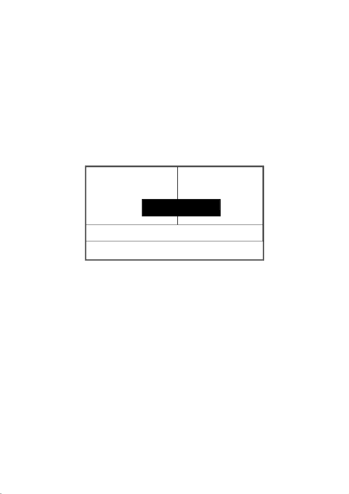
4.9 Load BIOS Defaults
When you press <Enter> on this item you will get a confirmation dialog
box with a message shown below. This option allows you to
load/restore the BIOS default values permanently stored in the BIOS
ROM. Pressing ‘Y’ loads the BIOS default values for the most stable,
minimal-performance system operations.
ROM PCI/ISA BIOS (2A434D2B)
LOAD BIOS DEFAULTS
AWARD SOFTWARE, INC.
STANDARD CMOS SETUP INTEGRATED PERIPHERALS
BIOS FEATURES SETUP SUPERVISOR PASSWORD
CHIPSET FEATURES SETUP USER PASSWORD
POWER MANAGEMENT SETUP IDE HDD AUTO DETECTION
PCI CONFIGURATION S ETUP
LOAD BIOS DEFAULTS
LOAD SETUP DEFAULTS
Esc : Quit
F10 : Save & Exit Setup (Shift) F2 : Change Color
Load BIOS Defaults (Y/N)? N
Load BIOS Defaults except Standard CMOS Setup
: Select Item
SAVING
47
Page 54
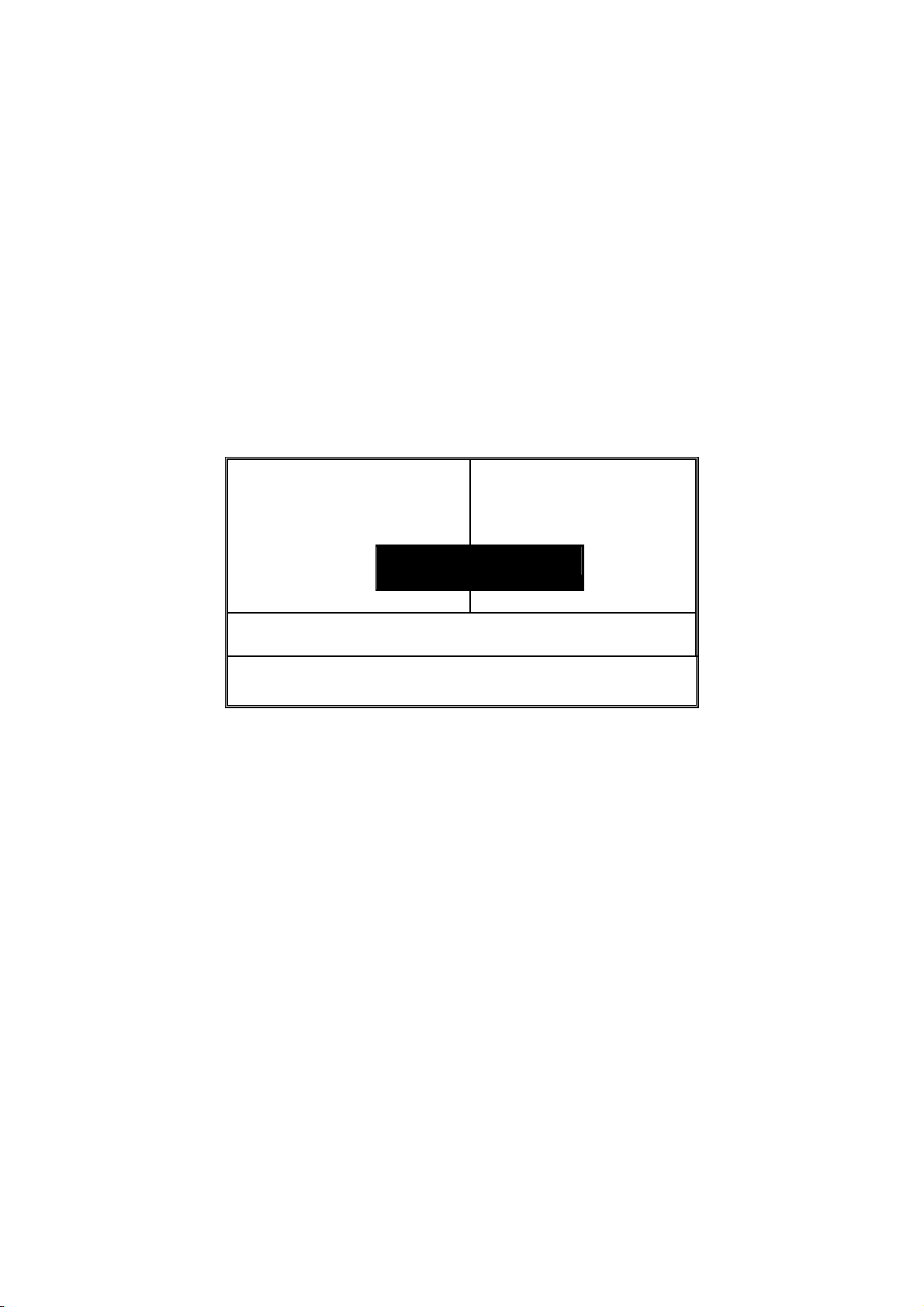
4.10 Load Setup Defaults
When you press <Enter> on this item you get a confirmation dialog box
with a message similar to the figure below. This option allows you to
load/restore the default values to your system configuration, optimizing
and enabling all high performance features. Pressing ‘Y’ loads the
default values that are factory settings for optimal performance system
operations.
ROM PCI/ISA BIOS (2A434D2B)
LOAD SETUP DEFAULTS
AWARD SOFTWARE, INC.
STANDARD CMOS SETUP INTEGRATED PERIPHERALS
BIOS FEATURES SETUP SUPERVISOR PASSWORD
CHIPSET FEATURES SETUP USER PASSWORD
POWER MANAGEMENT SETUP IDE HDD AUTO DETECTION
PCI CONFIGURATION S ETUP
LOAD BIOS DEFAULTS
LOAD SETUP DEFAULTS
Esc : Quit
F10 : Save & Exit Setup (Shift) F2 : Change Color
Load SETUP Defaults (Y/N)? N
Load BIOS Defaults except Standard CMOS Setup
: Select Item
SAVING
48
Page 55
4.11 Integrated Peripherals
The IDE hard drive controllers can support up to two separate hard
drives. These drives have a master/slave relationship that is
determined by the cabling configuration used to attach them to the
controller. Your system supports two IDE controllers--a primary and a
secondary--so you can install up to four separate hard disks.
PIO means Programmed Input/Output. Rather than having the BIOS
issue a series of commands to affect the transfer to or from the disk
drive, PIO allows the BIOS to tell the controller what it wants and then
let the controller and the CPU perform the complete task by them. This
is much simpler and more efficient (also faster).
ROM PCI/ISA BIOS (2A434D2B)
INTEGRATED PERIPHERALS
AWARD SOFTWARE, INC.
IDE HDD Block Mode : Enabled Parallel Port Mode : ECP+EPP
Primary IDE Channel : Enabled ECP Mode Use DMA : 3
Master Drive PIO Mode : Auto Onboard Serial Port 3 : 3E8
Slave Drive PIO Mode : Auto Serial Port 3 Use IRQ : IRQ10
Secondary IDE Channel : Enabled Onboard Serial Port 4 : 2E8
Master Drive PIO Mode : Auto Serial Port 4 Use IRQ : IRQ11
Slave Drive PIO Mode : Auto
Build in CPU Audio : Enabled
IDE Primary Master UDMA : Auto Audio I/O Base Address : 220H
IDE Primary Slave UDMA : Auto MPU-401 I/O Base Address : 330H
IDE Secondary Master UDMA : Auto Audio IRQ Select : IRQ 5
IDE Secondary slave UDMA : Auto Audio Low DMA Select : DMA 1
Audio High DMA Select : DMA 5
Joystick Status : Enabled
KBC input clock : 12MHz
Onboard FDC Controller : Enabled
Onboard Serial Port 1 : 3F8/IRQ4
On board Serial Port 2 : 2F8/IRQ3
UART2 Mode : Standard
ESC : Quit
F1 : Help PU/PD/+/-: Modify
F5 : Old Values (Shift) F2 : Color
F6 : Load BIOS Defaults
F7 : Load Setup Defaults
: Select Item
IDE HDD Block Mode:
This allows your hard disk controller to use the fast block mode to
transfer data to and from your hard disk drive (HDD).
Enabled IDE controller uses block mode
Disabled IDE controller uses standard mode
Primary/Secondary IDE Channel
You may separately disable the primary/second channel on an
IDE interface installed in a PCI expansion slot.
49
Page 56

IDE Primary/Secondary Master/Slave PIO Mode
The four IDE PIO (Programmed Input/Output) fields let you set a
PIO mode
(0-4) for each of the four IDE devices that the onboard IDE
interface supports.
Modes 0 through 4 provide successively increased performance.
In Auto mode, the system automatically determines the best mode
for each device.
IDE Primary/Secondary Master/Slave UDMA:
KBC Input Clock:
Onboard FDC Controller:
Onboard Serial Port 1/2/3/4:
UART2 Mode
Onboard Parallel Port:
Ultra DMA/33 is possible only if your IDE drive supports it and the
operating environment includes a DMA driver (Windows 95 OSR2
or a third-party IDE bus master driver). If your hard drive/system
software both support Ultra DMA/33, select Auto to enable BIOS
support.
The input clock setting of your onboard keyboard controller is set
from here.
Select Enabled if your system has a floppy disk controller (FDC)
installed on the system board and you wish to use it. If you install
and-in FDC or the system has no floppy drive, select Disabled in
this field. The available choices are Enabled, Disabled.
This item allows you to determine access onboard serial port
1/2/3/4 controller with which I/O address. The available choices
are 3F8/IRQ4, 2F8/IRQ3, 3E8/IRQ4, 2F8/IRQ3, Disabled, Auto.
Select the value required by the IR device connected to the IR
port. Full-duplex mode permits simultaneous two-direction
transmission. Half-duplex mode permits transmission in one
direction only at a time. The available choices are Half, Full.
Select a logical LPT port name and matching address for the
physical parallel (printer) port. The available choices are
378H/IRQ7, 278H/IRQ5, 3BCH/IRQ7, Disabled.
Parallel Port Mode:
Select an operating mode for the onboard parallel port. Select
Compatible or Extended unless you are certain both your
hardware and software support EPP or ECP mode. The available
choices are SPP, ECP+EPP1.7, EPP1.7+SPP, EPP1.9+SPP,
ECP, ECP+EPP1.9, and Normal.
ECP Mode Use DMA:
Select a DMA channel for the port. The available choices are 3, 1.
50
Page 57

Serial Port 3/4 Use IRQ:
This category assigns the interrupt request for both serial ports 3
and 4. The available options are 3F8/3, 3F8/4, 3F8/10, 3F8/11,
2F8/3, 2F8/4, 2F8/10, 2F8/11, 3E8/3, 3E8/4, 3E8/10, 3E8/11,
2E8/3, 2E8/4, 2E8/10, and 2E8/11.
Build in CPU Audio:
Audio I/O Base Address:
Audio IRQ Select:
Audio High DMA Select:
This item allows you to select the option of the build in CPU Audio
function. The available choices are Enable and Disable.
This chipset traps I/O accesses for Sound Blaster compatibility at
either 220H or 240H. The available choices are 220H, and 240H.
MPU-401 I/O Base Address:
This chipset traps I/O accesses for ROLAND MPU 401 UART
interface at 330H , 300H or Disable. The available choices are
330H, 300H, and Disable.
Select an interrupt for the audio port. The available choices are
IRQ 3, IRQ 5, IRQ 7, IRQ 10, and Disable .
Audio Low DMA Select:
This chipset supports I/O trapping for low DMA accesses and
allows you to select the Audio Low DMA type. The available
choices are DMA 0, DMA 1, DMA 3, and Disable.
This chipset supports I/O trapping for high DMA accesses and
allows you to select the Audio High DMA type. The available
choices are DMA 5, DMA 6, DMA 7, Disable.
51
Page 58
4.12 Supervisor/User Password Setting
ROM PCI/ISA BIOS (2A434D2B)
CMOS SETUP UTILITY
AWARD SOFTWARE, INC.
STANDARD CMOS SETUP INTEGRATED PERIPHERALS
BIOS FEATURES SETUP SUPERVISOR PASSWORD
CHIPSET FEATURES SETUP USER PASSWORD
POWER MANAGEMENT SETUP IDE HDD AUTO DETECTION
PNP/PCI CONFIGURA ETUP
LOAD BIOS DEFAULT
LOAD SETUP DEFAULTS
Esc : Quit
F10 : Save & Exit Setup (Shift) F2 : Change Color
Enter Password :
SAVING
: Select Item
Change / Set / Disable Password
You can set either supervisor or user password, or both of then. The
differences between are:
supervisor password: can enter and change the options of the setup
menus.
user password: just can only enter but do not have the right to change the
options of the setup menus.
When you select this function, the following message will appear at the
center of the screen to assist you in creating a password.
ENTER PASSWORD:
Type the password, up to eight characters in length, and press
<Enter>. The password typed now will clear any previously entered
password from CMOS memory. You will be asked to confirm the
password. Type the password again and press <Enter>. You may
also press <Esc> to abort the selection and not enter a password.
To disable a password, just press <Enter> when you are prompted to
enter the password. A message will confirm the password will be
disabled. Once the password is disabled, the system will boot and you
can enter Setup freely.
PASSWORD DISABLED.
52
Page 59
When a password has been enabled, you will be prompted to enter it
every time you try to enter Setup. This prevents an unauthorized
person from changing any part of your system configuration.
Additionally, when a password is enabled, you can also require the
BIOS to request a password every time your system is rebooted. This
would prevent unauthorized use of your computer.
You determine when the password is required within the BIOS
Features Setup Menu and its Security option (see Section 3). If the
Security option is set to “System”, the password will be required both at
boot and at entry to Setup. If set to “Setup”, prompting only occurs
when trying to enter Setup.
4.13 IDE HDD Auto Detection
This option detects the parameters of an IDE hard disk drive, and
automatically enters them into the Standard CMOS Setup screen.
Up to four IDE drives can be detected, with parameters for each
appearing in sequence inside a box. To accept the displayed entries,
press the “Y” key; to skip to the next drive, press the “N” key. If you
accept the values, the parameters will appear listed beside the drive
letter on the screen.
ROM PCI/ISA BIOS (2A434D2B)
CMOS SETUP UTILITY
AWARD SOFTWARE, INC.
HARD DISKS TYPE SIZE CYLS HEAD PRECOMP LANDZ SECTOR MODE
Primary Master:
Select Primary Master Option (N=SKIP) : N
OPTIONS TYPE SIZE CYLS HEAD PRECOMP LANDZ SECTOR MODE
1 (Y) 0 0 0 0 0 0 0 NORMAL
NOTE: Some OSes (like SCO-UNIX) must use ”NORMAL” for installation
53
Page 60
4.14 Save & Exit Setup
Pressing <Enter> on this item asks for confirmation: Pressing “Y”
stores the selections made in the menus in CMOS – a special section
of memory that stays on after you turn your system off. The next time
you boot your computer, the BIOS configures your system according to
the Setup selections stored in CMOS. After saving the values the
system is restarted again.
ROM PCI/ISA BIOS (2A434D2B)
CMOS SETUP UTILITY
AWARD SOFTWARE, INC.
STANDARD CMOS SETUP INTEGRATED PERIPHERALS
BIOS FEATURES SETUP SUPERVISOR PASSWORD
CHIPSET FEATURES SETUP USER PASSWORD
POWER MANAGEMENT SETUP IDE HDD AUTO DETECTION
PNP/PCI CONFIGURA ETUP
LOAD BIOS DEFAULT
LOAD SETUP DEFAULTS
Esc : Quit
F10 : Save & Exit Setup (Shift) F2 : Change Color
SAVE to CMOS and EXIT (Y/N)? N
Saves all Data & Exit Setup
SAVING
: Select Item
54
Page 61
4.15 Exit Without Saving
Pressing <Enter> on this item asks for confirmation:
Quit without saving (Y/N)? Y
This allows you to exit Setup without storing in CMOS any change. The
previous selections remain in effect. This exits the Setup utility and
restarts your computer.
ROM PCI/ISA BIOS (2A434D2B)
CMOS SETUP UTILITY
AWARD SOFTWARE, INC.
STANDARD CMOS SETUP INTEGRATED PERIPHERALS
BIOS FEATURES SETUP SUPERVISOR PASSWORD
CHIPSET FEATURES SETUP USER PASSWORD
POWER MANAGEMENT SETUP IDE HDD AUTO DETECTION
PNP/PCI CONFIGURA ETUP
LOAD BIOS DEFAULT
LOAD SETUP DEFAULTS
Esc : Quit
F10 : Save & Exit Setup (Shift) F2 : Change Color
Quit Without Saving (Y/N)? N
Abandon all Data & Exit Setup
SAVING
: Select Item
55
Page 62

This page intentionally left blank.
56
Page 63

Chapter 5
Software Utilities
This chapter contains the detailed information of VGA, Audio and LAN
driver installation procedures.
5.1 VGA Driver Installation for WIN95 &
WIN98
1. Click the
screen, then select
double-click on the
Properties
2. Select the setting page from the top menu then click on the
Advanced Properties
3. Select the
4. Click on the
all drivers in a specific location
you want.
5. Click on
checkbox and click on
6. Specify the path of the new driver and press
A:, select a:\win95)
7. The
8. Continue your selection until the program
you to restart your machine.
Start
button on the lower left hand corner of your
Setting
Display
window.
Change
Next
Select
device dialog box will appear. Select
button in the adapter area.
Next
button to continue. Select
to proceed. Select the
National Geode XpressGRAPHICS™
. Choose
icon to launch its
button.
Browse
.
Control Panel
Display a list of
, so you can select the drivers
Specify a location
Enter
FINISHES
and
Display
. (if in driver
and asks
57
Page 64
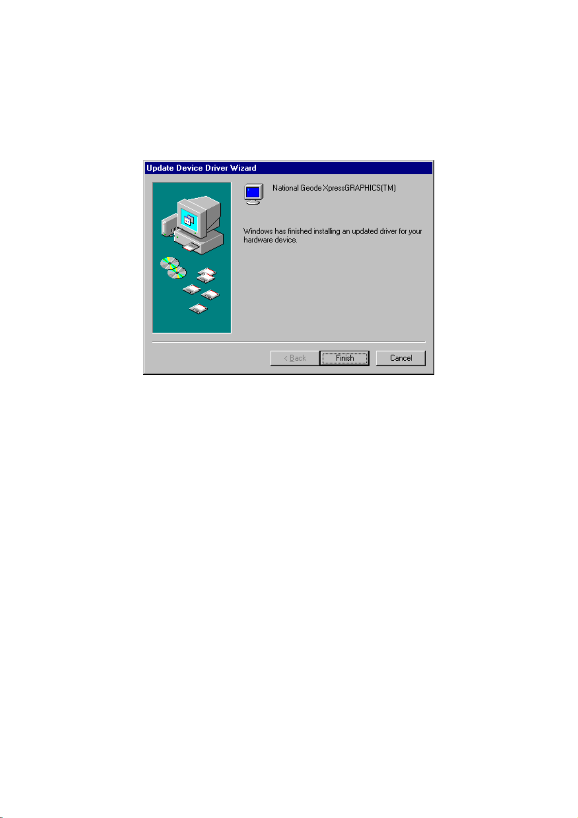
9. After the restarting your system, return to the display applet
(step 1) and select alternate screen resolutions and color
depths.
NOTE:
Installation procedure for Windows 98 is similar to Windows 95.
58
Page 65
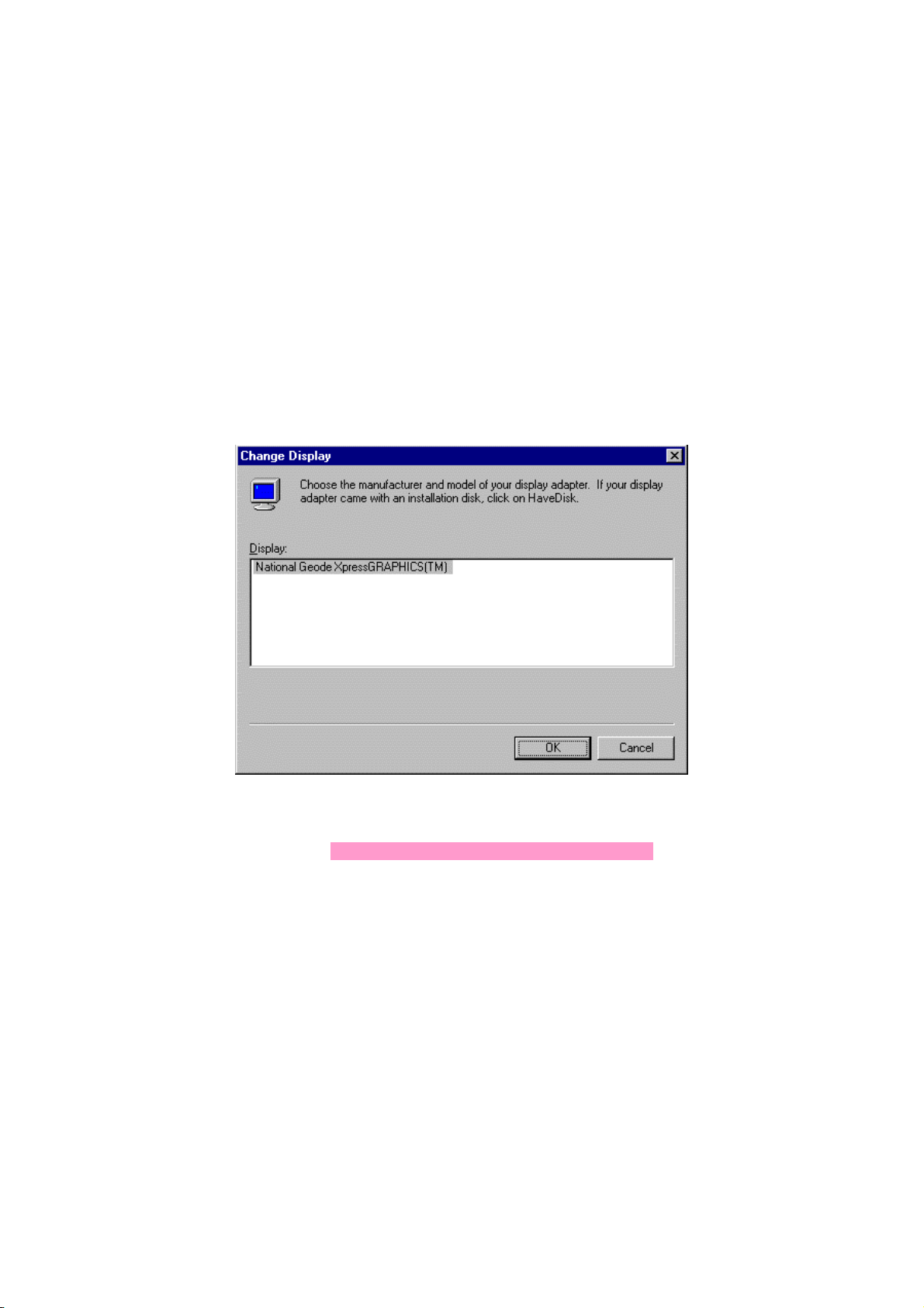
5.2 VGA Driver Installation for WIN
NT4.0
1. Click the
screen, then select
double-click on the
Properties
2. Click on the
3. In the
4. Specify the path of the new driver and then press on
driver A:, type a:\nt40)
5. Select
6. Click OK or press
7. You will see warning panel about
Yes
8. Once the installation is completed, you must shut down the
system and restart for the new driver to take effect.
Start
button on the lower left hand corner of your
Setting
Display
window.
Settings
Change Display Type
National Geode XpressGRAPHICS™
Enter
to finish the installation.
. Choose
tab, and then choose
.
Control Panel
icon to launch its
Display Type
window, click on
Third Party Drivers
and
Display
Have Disk
Enter
. (If in
. Click on
.
.
59
Page 66
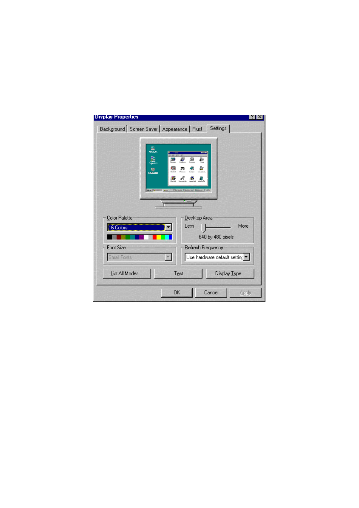
9. After restarting, check the VGA driver. The properties of the
driver should look similar with the following figure.
60
Page 67
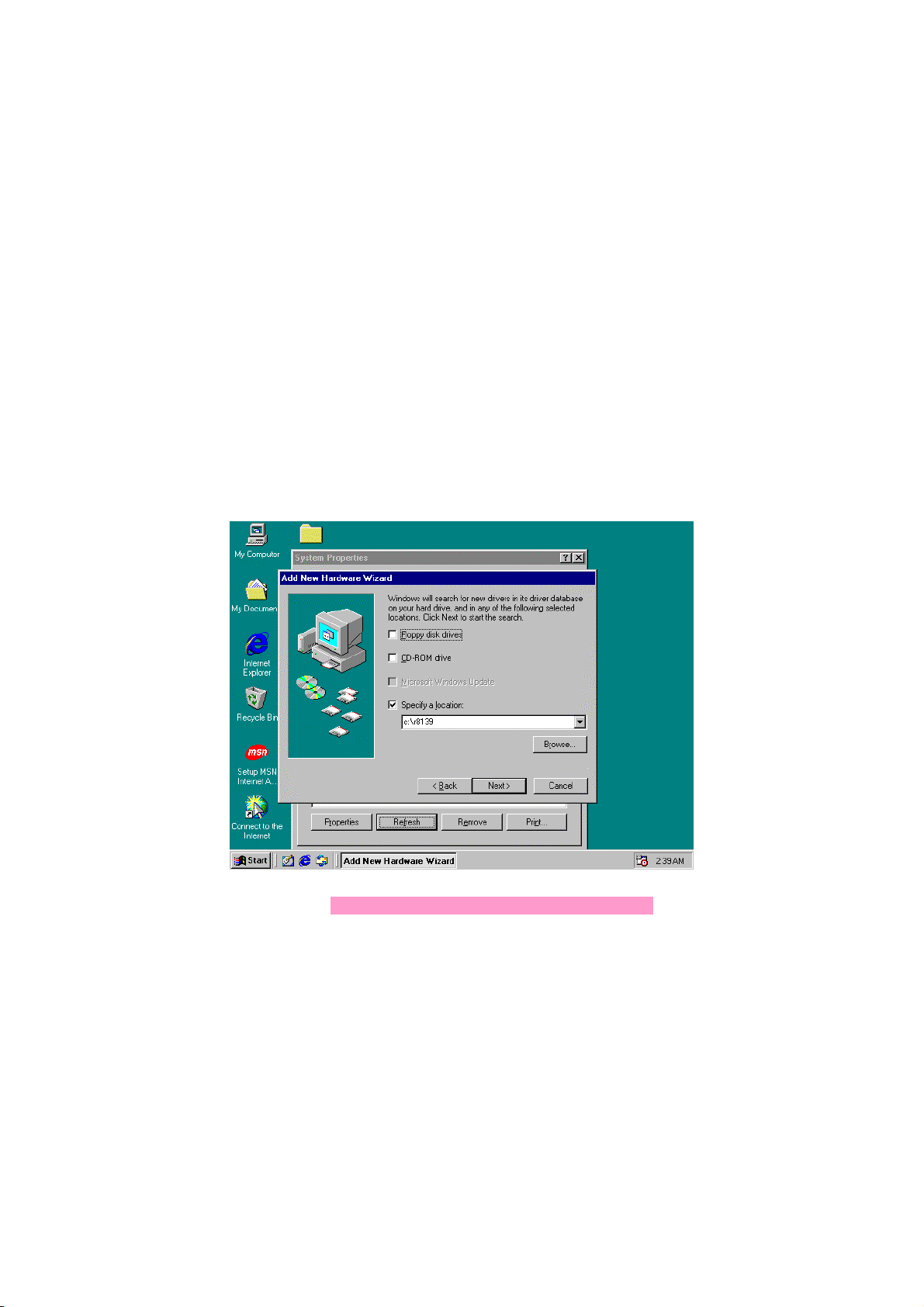
5.3 Network Driver Installation for
WIN98
1. Click the
screen, then select
double-click on the
applet window.
2. From the
3. In the
click
4. Specify the path of the new driver and press
a:, type a:\). If you’re not sure exactly where the drivers are,
choose the
Start
button on the lower left hand corner of your
Setting
Networks
Network
Select Network Component Type
Add
.
Browse
applet program, click on
button to locate it.
. Choose
Control Panel
icon to launch its
Add
, select
Enter
Network
.
Adapter
. (If in driver
and
then
5. Once you have located the drivers, select
RTL8139 Fast Ethernet Adapter
6. Click OK. Windows 98 will copy the network drivers to the
proper directories in your system.
61
Page 68
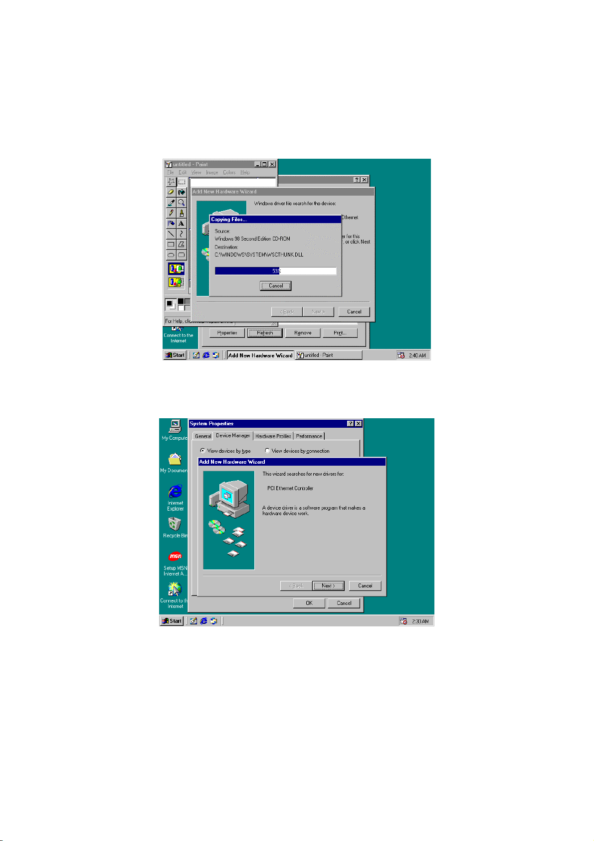
7. Continue clicking on OK until asked to restart your system.
8. After restarting, check on the network driver. Make sure the
Properties
figure.
of the driver should look similar with the following
NOTE:
62
RTL8139 driver installation program is similar with RTL8100’s.
Page 69
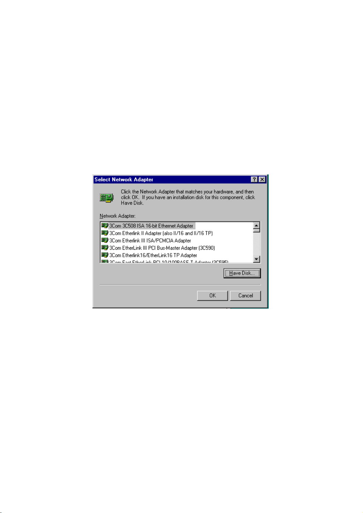
5.4 Network Driver Installation for WIN
NT4.0
1. Click the
Panel
2. Click on the
the
3. In the
This will bring up the
Start
.
Network
Adapters
Select Network Adapter
button, then go to
icon to start the Network window. Click on
tab, and then click on
Insert Disk
Settings
window, click on
window.
Add
.
and click on
Have Disk
Control
.
4. Specify the directory where the Windows NT driver files are
located. (If in driver A:, type a:\)
63
Page 70
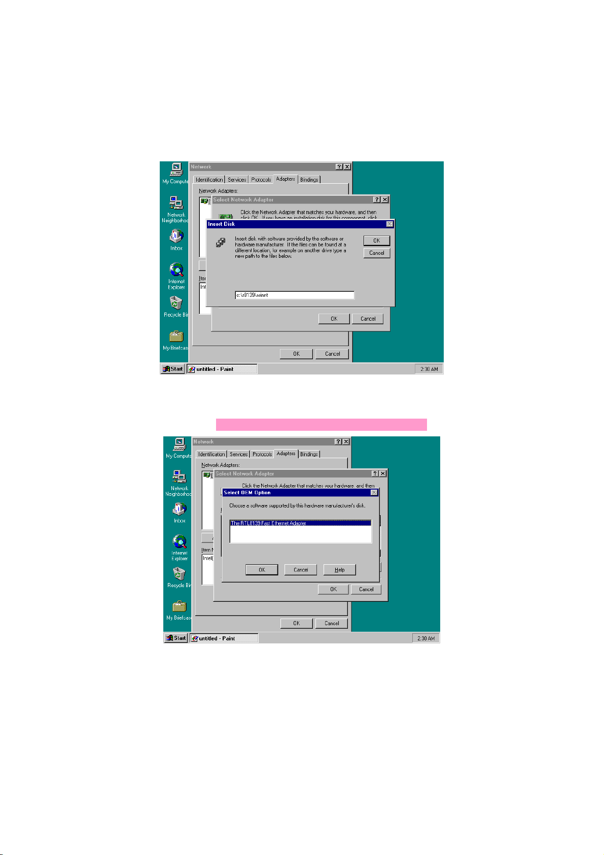
5. The
6. Select
Select OEM Option
screen.
window will then pop up on your
RTL8139 Fast Ethernet Adapter
7. Click OK to finish the installation process.
64
Page 71
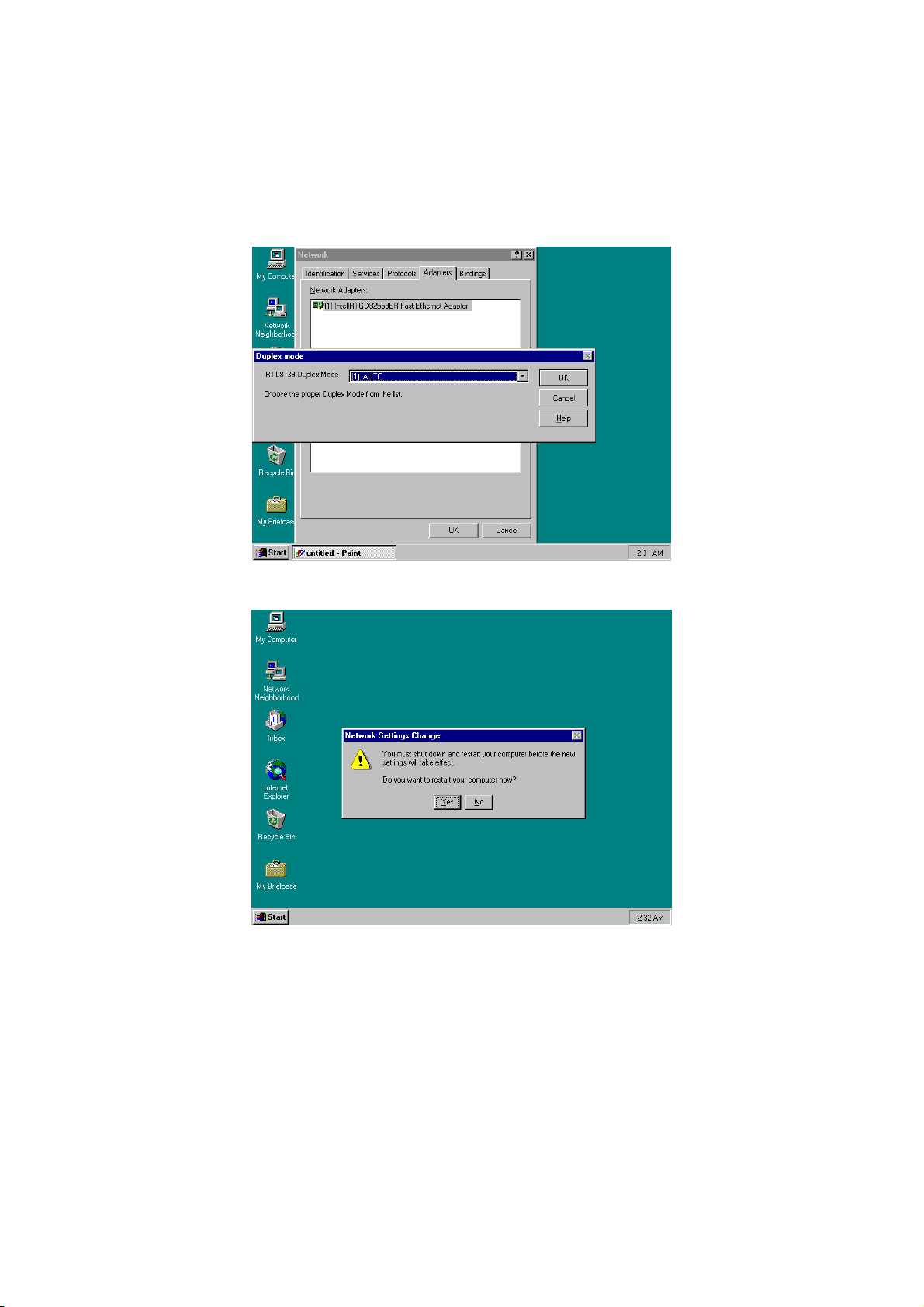
8. Once the installation is complete, the system must be shut down
and restarted for the new driver to take effect.
9. After restarting the system, check on the Network driver and
make sure that the
with the following figures.
NOTE:
RTL8139 driver installation program is similar with RTL8100’s.
Properties
of the driver should look similar
65
Page 72
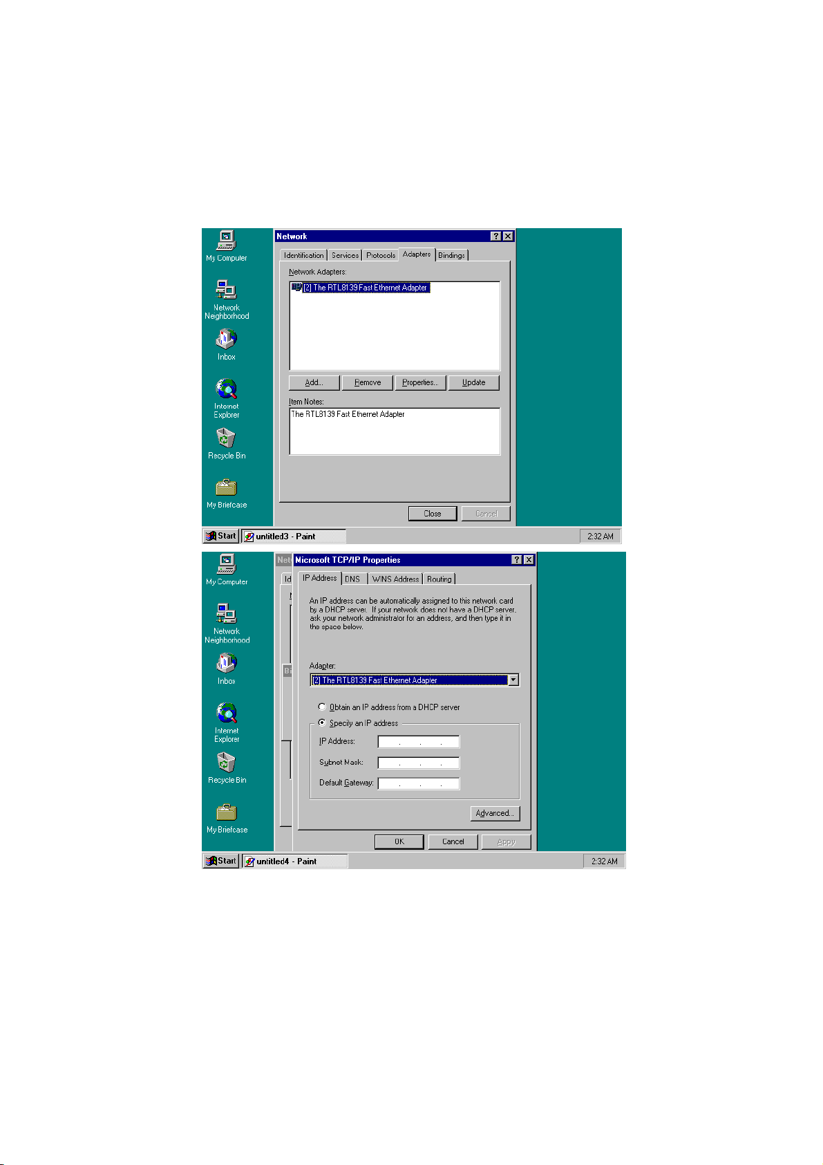
66
Page 73
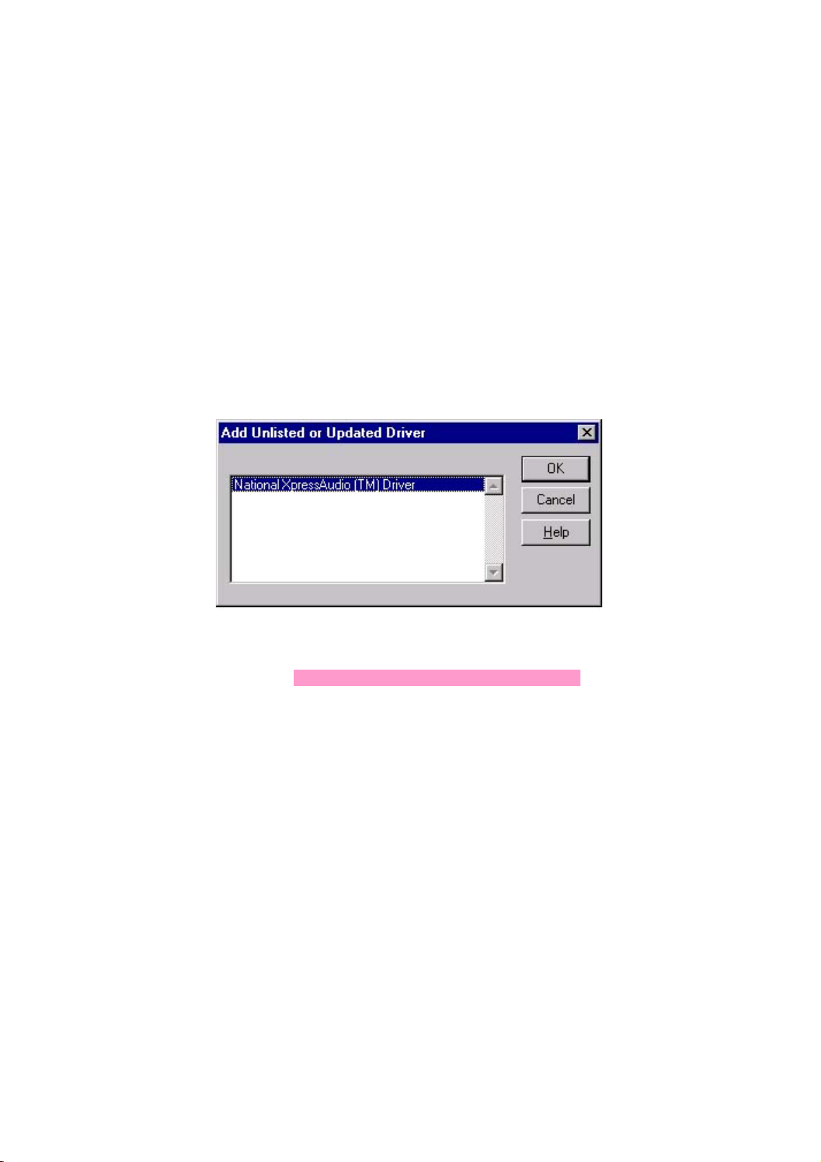
5.5 Audio Driver Installation for WIN
NT4.0
1. Click the
Panel
2. Click on the
3. Click on the
4. In the
properties.
5. Click on
6. Specify the path of the new driver and press
A:, type a:\nt40)
7. Select
8. Click OK or press
9. When you see
Continue to finish the installation.
10. Once the installation is completed, you must shut down and
restart the system for the new driver to take effect.
11. After restarting, check the audio driver. The properties of the
driver should look similar to the following figure.
Start
button, then go to
.
Display
Settings
Change Display Type
Unlisted or update driver
icon to launch the
tab, and then select on
National XpressAudio
Enter
.
National XpressAudio
Setting
window, click on
and click on
Multi Media Window
Multi Media Type
and press OK.
Enter
TM
Driver
TM
Driver
Control
Have Disk
. (If in driver
, click on
.
.
67
Page 74
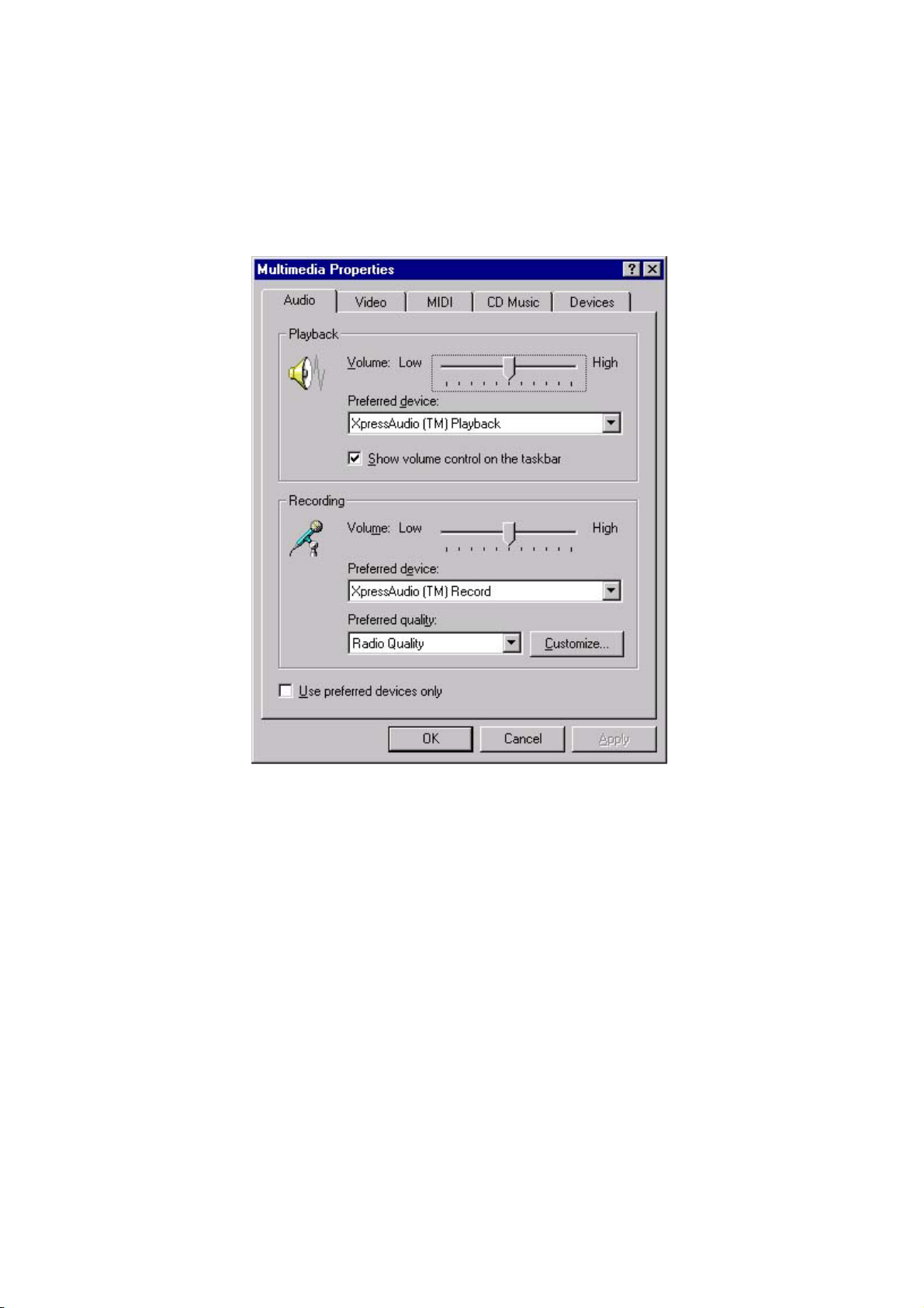
68
 Loading...