

Page 1

Contents
Safety Information............................................................................................................................ 2
Electrostatic Discharge Sensitive (ESDS) Device Handling ........................................................ 2
Jukebox Disassembly/Assembly Procedures............................................................................ 3-4
Jukebox Remote control ................................................................................................................. 5
Disassembly/Assembly Procedures .............................................................................................. 5
Figure 1. Remote Control Assembly Exploded View........................................................................ 5
Test Procedures ............................................................................................................................ 6-8
Part List Notes.................................................................................................................................. 9
Main Part List.................................................................................................................................... 9
Figure 2. Jukebox Assembly .......................................................................................................... 10
Figure 3. Woofer Wiring Diagram................................................................................................... 10
Figure 4. Rear Panel Assembly...................................................................................................... 11
Zone 1 Amp Electrical Part List ............................................................................................... 12-16
Zone 2 Amp Electrical Part List ............................................................................................... 17-19
I/O PCB Part List ....................................................................................................................... 20-22
Remote Control Part List............................................................................................................... 23
Figure 5. Remote Control Exploded View ...................................................................................... 23
®
JB Part List.............................................................................................................................. 24
141
Figure 6. 141JB Exploded View ..................................................................................................... 24
ZONE 2 Speaker Connections Greater Than 3.2
Figure 7. Zone 2 External Speaker Connections ........................................................................... 25
ZONE 2 Speaker Connections Less Than 3.2
Figure 8. Low DC Resistance Connections ................................................................................... 26
Figure 9. Low DC Resistance Connections ................................................................................... 26
Troubleshooting Tips..................................................................................................................... 27
Figure 10. Audio Section Wiring/Block Diagram ............................................................................ 28
Figure 11. Control Section Wiring/Block Diagram .......................................................................... 29
Cable Drawings ......................................................................................................................... 30-31
Ω ..................................................................... 25
Ω.......................................................................... 26
Caution: The TouchTunes Digital Jukebox contains no user serviceable parts. To prevent warranty infractions, refer servicing to warranty service stations or factory service.
PROPRIETARY INFORMATION
THIS DOCUMENT CONTAINS PROPRIETARY INFORMATION OF
BOSE® CORPORATION WHICH IS BEING FURNISHED ONLY FOR
THE PURPOSE OF SERVICING THE IDENTIFIED BOSE PRODUCT
BY AN AUTHORIZED BOSE SERVICE CENTER OR OWNER OF THE
BOSE PRODUCT, AND SHALL NOT BE REPRODUCED OR USED
FOR ANY OTHER PURPOSE.
1
Page 2

SAFETY INFORMATION
1. Parts that have special safety characteristics are identified by the symbol on
schematics or by special notes in the part lists. Use only replacement parts that
have critical characteristics recommended by the manufacturer.
2. Make leakage current or resistance measurements to determine that exposed
parts are acceptably insulated from the supply circuit before returning the unit
to the customer. Use the following checks to perform these measurements:
A. Leakage Current Hot Check: With the unit completely assembled, plug the AC line cord
directly into a 120V AC outlet. (Do not use an isolation transformer during this test.) Use a
leakage current tester or a metering system that complies with American National Standards
Institute (ANSI) C101.1 "Leakage Current for Appliances" and Underwriters Laboratories (UL)
813. With the unit's AC switch first in the ON position and then in the OFF position, measure
from a known earth ground (metal water pipe, conduit, etc.) to all exposed metal parts of the
unit (antennas, handle bracket, metal cabinet, screw-heads, metallic overlays, control shafts,
etc.), especially any exposed metal parts that offer an electrical return path to the chassis. Any
current measured must not exceed 0.75 milliamp. Reverse the unit's power cord plug in the
outlet and repeat the test. ANY MEASUREMENTS NOT WITHIN THE LIMITS SPECIFIED
HEREIN INDICATE A POTENTIAL SHOCK HAZARD THAT MUST BE ELIMINATED BEFORE RETURNING THE UNIT TO THE CUSTOMER.
B. Insulation Resistance Test Cold Check: (1) Unplug the power cord from the wall outlet
and connect a jumper wire between the two prongs of the plug. (2) Turn on the power switch of
the unit. (3) Measure the resistance with an ohmmeter between the jumpered AC plug and
each exposed metallic cabinet part on the unit. The reading should be between infinite. When
there is no return path to the chassis, the reading must be "infinite". If it is not within the limits
specified, there is the possibility of a shock hazard, and the unit must be repaired and rechecked before it is returned to the customer.
ELECTROSTATIC DISCHARGE SENSITIVE (ESDS)
DEVICE HANDLING
This unit contains ESDS devices. We recommend the following precautions when repairing,
replacing or transporting ESDS devices:
• Perform work at an electrically grounded work station.
• Wear wrist straps that connect to the station or heel straps that connect to conductive floor
mats.
• Avoid touching the leads or contacts of ESDS devices or PC boards even if properly
grounded. Handle boards by the edges only.
• Transport or store ESDS devices in ESD protective bags, bins, or totes. Do not insert
unprotected devices into materials such as plastic, polystyrene foam, clear plastic bags,
bubble wrap or plastic trays.
2
Page 3

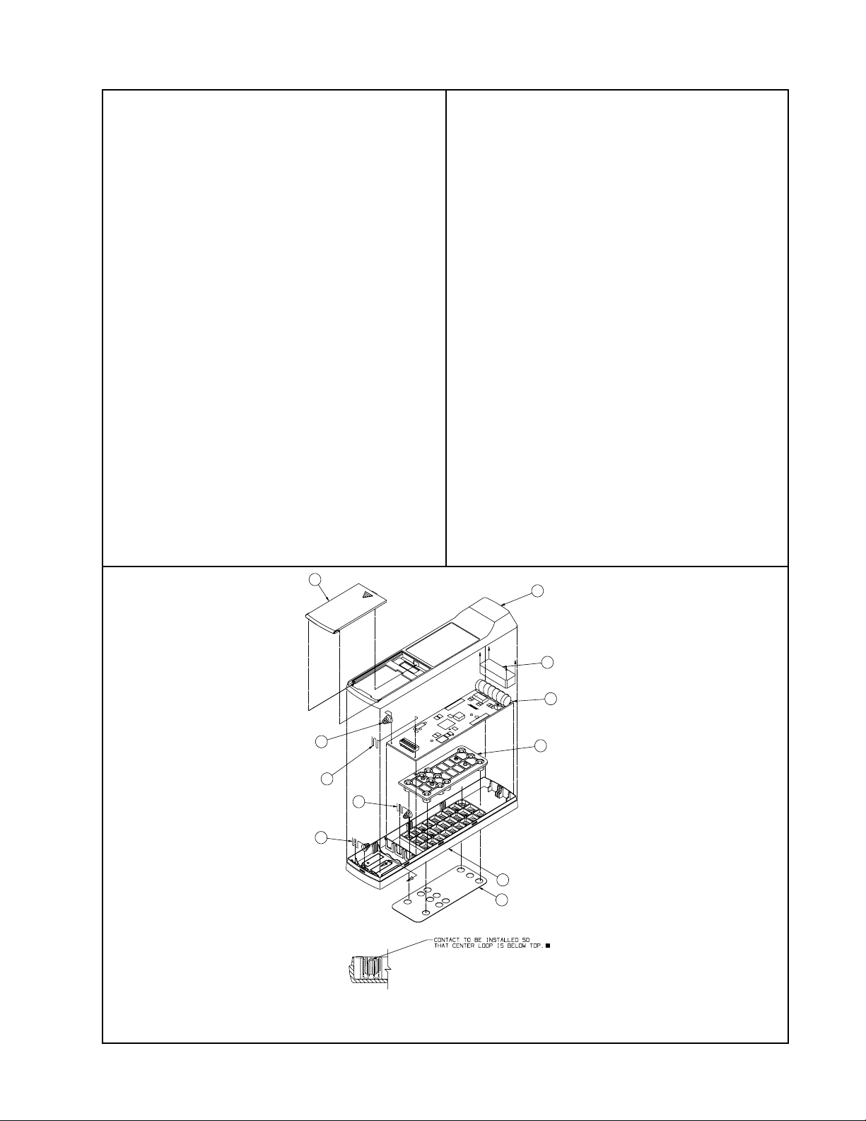
JUKEBOX DISASSEMBLY/ASSEMBLY PROCEDURES
Note: Refer to Figures 2 and 4.
1. Rear Panel Access
1.1 Using the Jukebox key, unlock the front
drawer and slide the front drawer out.
Note: Make sure that the shipping screw
has been removed.
1.2 Lift up the rear panel release handle
and push the handle toward the rear until
the handle locks into place.
Note: The rear panel can be fully opened
by removing the locking pin that secures
the rear panel release handle to the rear
panel.
2. Rear Panel Closure
2.1 Pull the rear panel release handle
forward until the rear panel is fully seated
and the release handle is locked in the
catch.
2.2 Slide the front drawer back into the
Jukebox and with the key, lock it into place.
3. Amplifier/EQ Module Removal
3.1 Perform procedure 1.
3.2 Remove the four screws (11) that
secure the bracket adaptor to the rear
panel and the lift off the bracket adaptor.
Note: If you are replacing the amplifier
assembly, perform procedure 5.2-5.3 and
save the adaptor bracket.
3.3 Located under the equalizer PCB and
the adaptor bracket is the amplifier assembly. Lift up the amplifier assembly to remove it.
3.4 Disconnect the transformer primary
(J7), transformer secondary (J1), RCA
output plugs (J9), DIN input plug (J5), AC
plug (J6) and the woofer output cable (J3)
(ZONE 1 only). Don't remove the interconnect cable between the equalizer PCB and
the amplifier assembly. Remove the entire
amplifier module (1, 2).
4. Amplifier/EQ Module Replacement
4.1 Align the amplifier assembly so that the
two posts on the rear panel line up with the
two grommets on the amplifier assembly.
Press firmly down on the amplifier assembly so that the two posts are fully inserted
into the two grommets.
4.2 Align the adaptor bracket with the screw
holes in the rear panel. See Figure 2 for the
correct position.
4.3 Connect all the connectors that were
removed in procedure 3.4.
4.4 Replace the four screws (11) that
secure the adaptor bracket to the rear
panel.
5. Fuse Access/EQ PCB Removal
5.1 Perform procedure 1.
5.2 Remove the screw (14) that secures
the equalizer PCB to the bracket adaptor.
5.3 Press outward on the four tabs that
secure the equalizer PCB to the bracket
adaptor. Lift off the equalizer PCB. The
fuse is located on the under side of the
equalizer PCB.
6. EQ PCB Replacement
6.1 Line up the slots on the equalizer PCB
with the tabs on the adaptor bracket.
6.2 Replace the screw (14) that secures the
equalizer PCB to the adaptor bracket.
7. I/O PCB Removal
7.1 Perform procedure 1.
7.2 Remove the four screws (12) that
secure the I/O PCB to the rear panel.
7.3 Remove all the connectors from the I/O
PCB. Make a note of the wire configuration.
Lift up the I/O PCB.
3
Page 4

JUKEBOX DISASSEMBLY/ASSEMBLY PROCEDURES
Note: Some units have the antenna cable
soldered to the I/O PCB.
8. I/O PCB Replacement
8.1 Align the I/O PCB so that the holes in the
I/O PCB align with the locator pins on the
rear panel. Press down on the I/O PCB until
the locator pins are fully inserted through the
holes in the I/O PCB.
8.2 Replace the four screws (12) that secure
the I/O PCB to the rear panel.
8.3 Connect all the connectors that were
removed in procedure 5.3.
Note: The modem plug that connects to the
computer connects to J9. Solder the antenna cable to the I/O PCB if it was initially
soldered.
9. Transformer Removal
11.2 Lift the 141JB out of the Jukebox and
remove the wires from the rear of the
enclosure.
12. 141JB Replacement
12.1 Attach the wires to the rear of the
141JB (6).
12.2 Line up the inserts in the 141JB with
the screw holes in the Jukebox.
12.3 Replace the two wing nuts that secure
the 141JB to the Jukebox.
13. Woofer Removal
13.1 Perform Procedure 1.1.
13.2 Remove the 10 screws (10) that
secure the woofer access panel to the
Jukebox. Pull off the access panel.
9.1 Cut the wire ties that secure the transformer wire harness.
9.2 Disconnect the primary (J7) and secondary (J1) connectors from the amplifier
module (1, 2).
9.3 Remove the four nuts (13) that secure
the transformer to the rear panel. Lift the
transformer up (4).
10. Transformer Replacement
10.1 Align the transformer with the screw
posts on the rear panel.
10.2 Replace the four nuts (13) that secure
the transformer to the rear panel.
10.3 Connect the primary (J7) and secondary (J1) connectors to the amplifier module
(1, 2). Replace the wire ties that were
removed in procedure 7.1.
®
11. Detachable 141
JB Removal
13.3 Remove the four screws (9) that
secure the woofer (8) to the Jukebox.
13.4 Lift the woofer out of the Jukebox and
cut the wires as close as possible to the
woofer. Make a note of the wire configuration.
14. Woofer Replacement
14.1 Attach the wires to the replacement
woofer (8) referring to the wire configuration notes taken in procedure 11.4 and
figure 3.
14.2 Align the woofer to the Jukebox and
twist any excess wire to prevent wire
buzzes.
14.3 Replace the four screws (9) that
secure the woofer to the Jukebox.
14.4 Align the woofer access panel to the
Jukebox and replace the 10 screws (10)
that secure it to the Jukebox.
11.1 Remove the two wing nuts located on
the side of the 141JB (6).
4
Page 5
JUKEBOX REMOTE CONTROL
DISASSEMBLY/ASSEMBLY PROCEDURES
1. Enclosure Disassembly
1.1 Slide off the battery compartment door
(5) and remove the batteries.
1.2 While holding the top cover (4) with one
hand, place your fingers of your other hand
in the battery compartment and grasp the
lower part of the bottom cover (3) with your
fingers.
1.3 With your fingertips in the battery compartment, first pull parallel to the unit and
then pull perpendicular.
1.4 With the catches released at the bottom,
work your fingers up the sides to release
the rest of the catches.
2. Enclosure Assembly
2.1 Lower the bottom cover (3) onto the top
cover (4) so that the bottom cover's lip fits
over the top cover.
2.2 Press the top cover and the bottom
cover together until they snap into place.
3. PCB Removal
3.1 Lift the PCB (1) straight up. The springs
will come up with the PCB.
4. PCB Replacement
4.1 Lower the PCB (1) into the top cover (4)
so that the springs are in the battery compartment.
5. Pad Removal
5.1 The pad (2) is not secured. Grasp a
corner of the pad and lift it out.
6. Pad Replacement
6.1 Lower the pad (2) into the top cover (4)
so that the buttons line up with the holes in
the top cover.
5
6
7
9
8
B
B
3
12
1
2
4
10
SECTION B-B
Figure 1. Remote Control Assembly Exploded View
5
Page 6
TEST PROCEDURES
Note: The following tests are intended to
be used by a qualified electronic technician
to service an amplifier module. These
procedures are not intended to be used in
the field.
ZONE 1 Bass Channel Test Procedures
Note: Use the AM-5
number 172296, to connect the test equipment to the input (J5) of the amplifier. Disconnect the speakers from the amplifier outputs
and do not load the outputs unless otherwise
noted.
Unit Turn On Procedure
Apply 12 VDC to J5 pin1 (refer to the
schematic). This will simulate the turn-on
signal the amplifier receives from the
computer.
1. Bass Channel DC Offset
®
P audio input cable, part
4.2 Reference a dB meter to the woofer
channel output.
4.3 Measure the woofer output according to
the following table.
Frequency Output Tolerance
20 Hz -21.3 dB ± 2.0 dB
40 Hz +3.0 dB ± 1.5 dB
100 Hz Reference 200 Hz -24.5 dB ± 2.0 dB
5. Bass Channel Dynamic Equalizer Gain
5.1 Apply a 2.4 mVrms, 50 Hz signal to the
left and right input.
5.2 Reference a dB meter to the bass
channel output.
5.3 Apply a 240 mVrms, 50 Hz signal to the
left and right input.
1.1 Disconnect all audio input signals.
1.2 Measure the woofer channel output. It
should be 0 ± 70 mVDC.
2. Bass Channel Output Noise
2.1 Short all audio inputs.
2.2 Measure the woofer channel output. It
should be <10 mVrms.
3. Bass Channel Reference Gain
3.1 Apply a 200 mVrms, 100 Hz signal to
the left and right input.
3.2 Reference a dB meter to the applied
signal.
3.2 Measure the bass channel output. It
should be 28.3 dB ± 1.5 dB.
5.4 Measure the bass channel output. It
should be 26.3 dB ± 1.5 dB (referenced to
the measurement taken in 5.2).
6. Bass Channel Small Signal Distortion at
0.5 W (1.414 Vrms)
6.1 Connect the speaker or a 6 Ω, 1%,
100 W resistive load to the bass channel
output.
6.2 Apply a 54 mVrms, 100 Hz signal to the
left and right input.
6.3 Measure the distortion at the bass
channel output. It should be <0.5% THD.
7. Bass Channel Large Signal Distortion at
80 W (17.9 Vrms)
7.1 Connect the speaker or a 6 Ω, 1%,
resistive load to the bass channel output.
4. Bass Channel Relative Frequency
Response
4.1 Apply a 200 mVrms, 100 Hz signal to
the left and right input.
7.2 Apply a 685 mVrms, 100 Hz signal to
the left and right input.
7.3 Measure the distortion at the bass
channel output. It should be <0.2% THD.
6
Page 7
TEST PROCEDURES
8. Bass Control Test
8.1 Apply a 50 mVrms, 100 Hz signal to the
left and right input.
8.2 Adjust R302 to center. Reference a dB
meter to the bass channel output.
8.3 Adjust R302 to maximum. Measure the
bass channel output. It should be +2.5 dB ±
1.5 dB.
8.4 Adjust R302 to minimum. Measure the
bass channel output. It should be -2.8 dB ±
1.5 dB.
9. Bass Compressor Test
9.1 Apply a 1.4 mV rms, 100 Hz signal to
the left and right input.
9.2 Measure the distortion at the bass
channel output. It should be <10% THD.
ZONE 1 and 2 Left/Right Channel Tests
Note: Unload the amplifier outputs unless
otherwise noted.
Unit Turn On Procedure
Apply 12 VDC to J5 pin1. This will simulate
the turn on signal the amplifier receives
from the computer.
12. Left/Right Reference Gain
12.1 Apply a 200 mVrms, 1.0 kHz signal to
the left/right input.
12.2 Measure the left/right channel output.
It should be (19.2 dB ± 1.5 dB, ZONE 1)
(34.0 dB ± 1.5 dB, ZONE 2).
13. ZONE 1 Left/Right Channel Relative
Frequency Response
13.1 Apply a 200 mVrms, 1.0 kHz signal to
the left/right channel output.
13.2 Reference a dB meter to the left/right
channel output.
13.3 Measure the left/right channel output
according to the following table.
Frequency Output Tolerance
100 Hz -1.8 dB ± 2.5 dB
170 Hz +6.4 dB ± 1.0 dB
600 Hz +2.5 dB ± 1.0 dB
1 kHz Reference -
1.4 kHz +0.6 dB ± 1.0 dB
6.0 kHz +10.5 dB ± 1.0 dB
12 kHz +14.2 dB ± 1.5 dB
20 kHz +6.6 dB ± 3.0 dB
14. ZONE 2 Left/Right Channel Relative
Frequency Response
10. Left/Right DC Offset
10.1 Disconnect all audio input signals.
10.2 Measure the left/right channel output.
It should be 0 ± 70 mV.
11. Left/Right Output Noise
11.1 Disconnect all audio input signals.
11.2 Measure the left/right channel output.
It should be ≤500 µV un-weighted.
14.1 Apply a 50 mVrms, 1 kHz signal to left/
right channel input.
14.2 Reference a dB meter to the left/right
channel output.
14.3 Measure the left/right channel output
according to the following table.
Frequency Output
20 Hz -0.6 ± 1.0 dB
20 kHz -0.6 ± 1.0 dB
7
Page 8

TEST PROCEDURES
15. Left/Right Channel Small Signal Distortion at (0.1 W, 632 mVrms ZONE 1) (0.5
W, 1.4 Vrms ZONE 2)
15.1 Connect a 4 Ω, 1%, 50 W resistive
load to the left/right channel output.
15.2 Apply a (25 mVrms ZONE 1) (28
mVrms ZONE 2), (4 kHz ZONE 1) (9 kHz
ZONE 2) signal to the left/right input.
15.3 Measure the distortion at the left/right
channel output. It should be <0.2% THD.
16. Left/Right Channel Large Signal Distortion at (30 W, 15.5 Vrms ZONE 1) (30 W,
11.0 Vrms ZONE 2)
16.1 Connect a 4 Ω, 1%, 50 W resistive
load to the left/right channel output.
16.2 Apply a (1.7 Vrms ZONE 1) (220
mVrms ZONE 2), 1 kHz signal to the left/
right input.
19. Short Circuit Protection Test
19.1 Apply a (1 Vrms ZONE 1) (0.35
mVrms ZONE 2), 1 kHz signal to the left/
right channel input.
19.2 Momentarily short the left channel.
19.3 Verify that the mute line (J2 pin 5)
goes low (<0.2 V). Wait three seconds and
repeat for the right channel.
16.3 Measure the distortion at the left/right
channel output. It should be <0.2% THD.
17. Left/Right Channel Separation
17.1 Apply a 100 mVrms, 10 kHz signal to
the right (left) channel only. Short the left
(right) channel input.
17.2 Reference a dB meter to the right (left)
channel.
17.3 Measure the left (right) channel output. It should be <-30 dB.
18. Compressor Test
18.1 Apply a (1.9 Vrms ZONE 1) (0.70
Vrms ZONE 2), 1 kHz, signal to the left and
right channel input.
18.2 Measure the distortion at the left and
right output. It should be <6.0%
8
Page 9
PART LIST NOTES
AMP ASSY, ZONE 1, 115V PART NUMBER 199018-9014 USES PCB ASSY 195225
AMP ASSY, ZONE 2, 115V PART NUMBER 199019-9014 USES PCB ASSY 195178
1. This part is not normally available from customer service. Approval from the Field Service
Manager is required before ordering.
2. The individual parts located on the PCB are listed in the part list.
3. This part is critical for safety purposes. Failure to use a substitute replacement with
the same safety characteristics as the recommended replacement part might create shock, fire
and/or other hazards.
MAIN PART LIST
Item
Number
1 AMP ASSY, ZONE 1, 115VAC 199018-9014
2 AMP ASSY, ZONE 2, 115VAC 199019-9014
3 PCB ASSY, I/O 250636-9014
4 TRANSFORMER, 120V 196196 3
5 FAN, 115VAC 196882 3
6
7 WOOFER 190170
- FILTER, FAN 196829-001
- REMOTE CONTROL 199640-9014
®
141
JB, PAIR, DETACHABLE
Description Part Number Note
250637-9014
9
Page 10
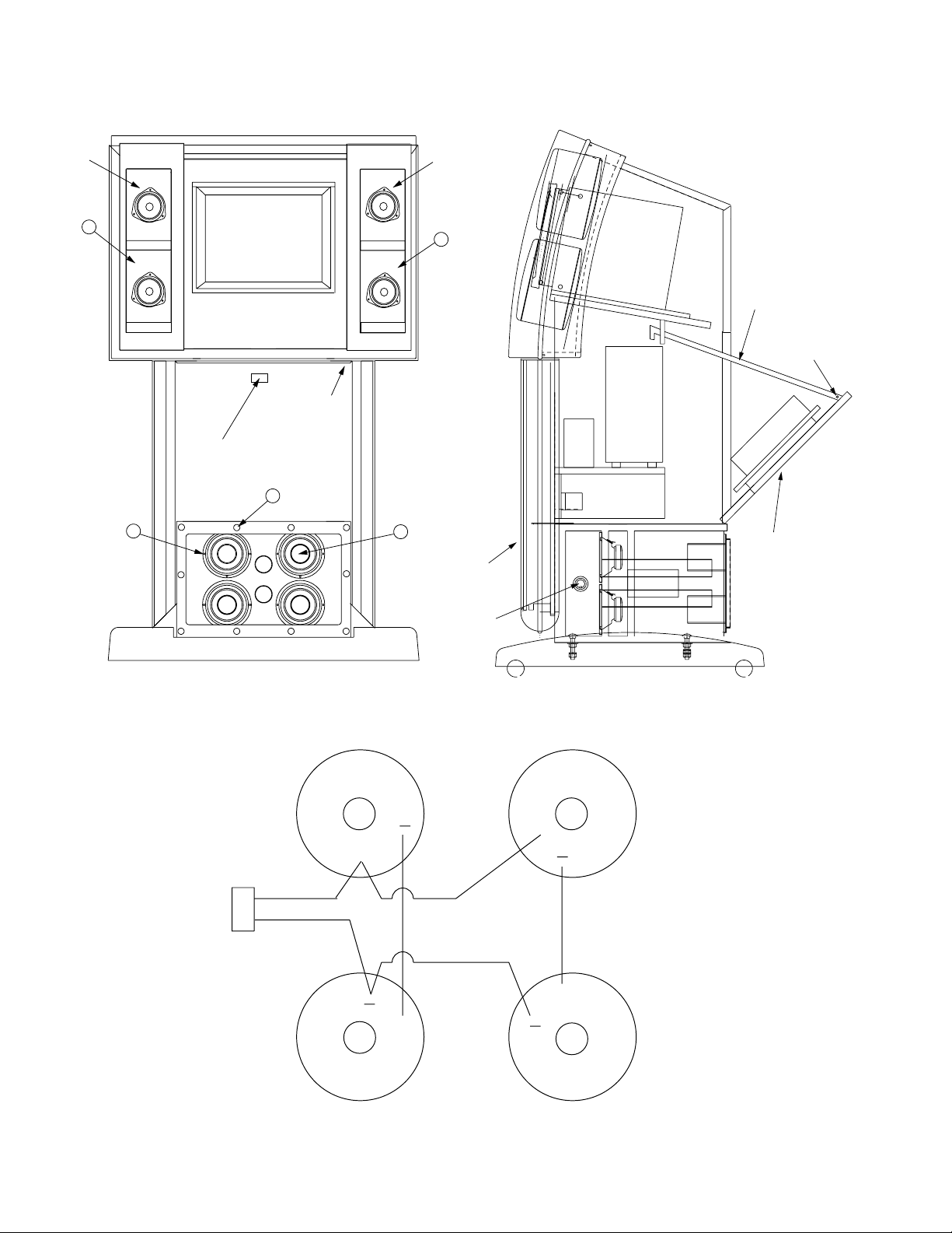
Fixed
Fixed
Detachable
6
Top Panel
Latch (x2)
Rear Panel
Release Handle
10
9
View without Front Drawer
8
6
Detachable
Front
Drawer
Front
Drawer
Lock
UPS
Computer
Rear Panel
Release Bar
Retaining Pin
AMP
Rear Panel
Assembly
red
black
Figure 2. Jukebox Assembly
+
+
yellow
grey
green
grey
+
+
Figure 3. Woofer Wiring Diagram
10
Page 11

4
4
WOOFER
OUTPUT
(J3)
(ZONE 1 ONLY)
13
Locator
Pin
12
ZONE 2
XFORMER
AC
3
I/O PCB
ZONE 1
XFORMER
FAN
5
XFORMER
INPUT
RCA
OUTPUT
PRIMARY
(J7)
DIN
(J5)
(J9)
ZONE 1
AMP
FUSE
(bottom side)
INPUT
14
ZONE 2
AMP
AC
(J6)
1
Bracket
Adaptor
2
11
Locator
Pin
11
12
XFORMER
SECONDARY
(J1)
Figure 4. Rear Panel Assembly
11
Page 12

ZONE 1 AMP ELECTRICAL PART LIST
Resistors
Reference Designator Description Part Number Note
R2, 10, 375 14.3k, 1206, 1/8W, 1% 124894-1432
R3, 4, 8, 12, 22, 23, 176, 190, 192,
276, 290, 292, 384
R5, 6, 393 5.1Ω, LEADED, FUSE,
R7, 24, 25 20.0k, 1206, 1/8W, 5% 124895-2035
R9 30.1k, 1206, 1/8W, 1% 124894-3012
R11 THERMISTOR, 20k, ERT-
R101, 102, 103, 104, 115, 201, 202,
203, 204, 215, 417, 422, 425, 439, 459,
460
R105, 106, 205, 206 2.49k, 0805, 1/10W, 1% 133625-2491
R107, 120, 140, 207, 220, 240, 414,
419, 433
R108, 208, 317 147Ω, 0805, 1/10W, 1% 133625-1470
R109, 129, 138, 196, 209, 229, 238,
296, 322, 331, 333, 346
R110, 210 2.55k, CHIP, 0805, 1/10W,
R111, 112, 211, 212 10.0k, 0805, 1/10W, 1% 133625-1002
R114, 214, 312 22.1k, 0805, 1/10W, 1% 133625-2212
R116, 216 5.11k, CHIP, 0805, 1/10W,
R117, 139, 217, 239 1.54k, 0805, 1/10W, 1% 133625-1541
R118, 126, 133, 134, 218, 226, 233,
234
R119, 219 3.16k, 0805, 1/10W, 1% 133625-3161
R121, 221 1.05k, 0805, 1/10W, 1% 133625-1051
R122, 137, 222, 237 10Ω, CHIP, 0805, 5% 133626-1005
R124, 224 7.15k, 0805, 1/10W, 1% 133625-7151
R125, 130, 225, 230 9.09k, 0805, 1/10W, 1% 133625-9091
R127, 227 681Ω, CHIP, 0805, 1/10W,
R131, 231, 432 20.0k, CHIP, 0805, 1/10W,
R132, 232 432Ω, CHIP, 0805, 1/10W,
R135, 136, 235, 236, 304, 329, 330,
411
R141, 241, 323, 324, 327, 328 100k, 0805, 1/10W, 1% 133625-1003
R143, 149, 243, 249, 303, 305, 337,
344, 404, 415, 416, 418, 420, 421, 423,
429, 431, 457, 458
R174, 274, 374 5.90k, 1206, 1/8W, 1% 124894-5901
R175, 275 1.80k, 1206, 1/8W, 5% 124895-1825
R177, 277, 381, 385 2.49k, 1206, 1/8W, 1% 124894-2491
R178, 179, 278, 279, 399 49.9k, 1206, 1/8W, 1% 124894-4992
R180, 185, 280, 285, 378, 380, 387,
394
R181, 183, 186, 188, 189, 191, 281,
283, 286, 288, 289, 291, 388, 389, 396,
397
R182, 187, 282, 287 7.50k, 1206, 1/8W, 1% 124894-7501
R184, 193, 284, 293, 392 220Ω, CF, 5%, 52mm 121243-1212215
10.0k, 1206, 1/8W, 5% 124895-1035
130102-5R1 3
1/4W
177557
D3FHL203S
1.00k, CHIP, 0805, 1/10W,
1%
10.0k, 0805, 1/10W, 5% 133626-1035
JUMPER, CHIP, 0805 133627
1%
1%
11.8k, 0805, 1/10W, 1% 133625-1182
1%
1%
1%
330Ω, 0805, 1/10W, 5% 133626-3315
100k, 0805, 1/10W, 5% 133626-1045
100k, 1206, 1/8W, 5% 124895-1045
1.00k, 1206, 1/8W, 5% 124895-1025
133625-1001
133625-2551
133625-5111
133625-6810
133625-2002
133625-4320
12
Page 13

ZONE 1 AMP ELECTRICAL PART LIST
Resistors (continued)
Reference Designator Description Part Number Note
R194, 294 0.1Ω, 2512, 1W, 5% 149322-100
R301 18.7k, CHIP, 0805, 1/10W,
1%
R302 POT., DUAL, 10k,
DETENT.
R306, 376, 424, 430 1M, 0805, 1/10W, 5% 133626-1055
R309, 434, 436 2.00k, 0805, 1/10W, 1% 133625-2001
R310 86.6k, 0805, 1/10, 1% 133625-8662
R311, 315 23.7k, 0805, 1/10W, 1% 133625-2372
R313, 413 12.1k, 0805, 1/10W, 1% 133625-1212
R314, 401, 410 100Ω, CHIP, 0805, 1/10W,
5%
R316, 318, 402 1.62k, 0805, 1/10W, 1% 133625-1621
R320 5.36k, 0805, 1/10W, 1% 133625-5361
R321 23.2k, 0805, 1/10W, 1% 133625-2322
R325 4.75k, 0805, 1/10W, 1% 133625-4751
R326 17.4k, 0805, 1/10W, 1% 133625-1742
R336 3.0k, CHIP, 0805, 1/10W,
5%
R377 301Ω, 1206, 1/8W, 1% 124894-3010
R379 10M, 1206, 1/8W, 5% 124895-1065
R382 200Ω, 1206, 1/8W, 5% 124895-2015
R383 200k, 1206, 1/8W, 1% 124894-2003
R386 4.22k, 1206, 1/8W, 1% 124894-4221
R390, 395 75Ω, CF, 5%, 1/4W, 52mm 121243-1217505
R398 33.2k, 1206, 1/8W, 1% 124894-3322
R412 39Ω, CF, 1/4W, 5%, 52mm 121243-1213905 3
133625-1872
185173
133626-1015
133626-3025
R426, 428, 435 20k, CHIP, 0805, 5% 133626-2035
R432 3.01k, 0805, 1/10W, 1% 133625-3011
R438 196Ω, 0805, 1/10W, 1% 133625-1960
R448 14.3k, 0805, 1/10W, 1% 133625-1432
R455 36.5k, 0805, 1/10W, 1% 133625-3652
R456 SUPPRESSOR 180580-01 3
Capacitors
Reference Designator Description Part Number Note
C1, 5, 6, 11, 12, 15, 16, 17, 18, 185,
285, 379, 380, 381
C3, 4 4700uF, EL, BP, 85, 50V,
C7, 8 4700uF, EL, 85, 25V, 20% 170216
C9, 10, 13, 14, 101, 102, 175, 176,
201, 202, 275, 276, 302, 303, 304, 409,
427
C103, 130, 131, 203, 230, 231, 301,
426
C104, 204 47uF, EL, 105, 16V, 20% 137126-470
C106, 206 .015uF, BOX, 85, 100V, 5% 137127-153
C107, 108, 207, 208, 309, 310, 314,
315
C109, 110, 209, 210 .018uF, BOX, 85, 100V, 5% 137127-183
.1uF, 1206, Y5V, 50V, 80% 138551-104
187394
20%
10uF, EL, 105, 16V, 20% 137126-100
100pF, 0805, COG, 50V,
5%
.47uF, BOX, 85, 50V, 5% 137127-474
133622-101
13
Page 14

ZONE 1 AMP ELECTRICAL PART LIST
Capacitors (continued)
Reference Designator Description Part Number Note
C112, 212 .18uF, BOX, 85, 50V, 5% 137127-184
C113, 114, 118, 119, 213, 214, 218,
219
C115, 116, 215, 216 .0082uF, BOX, 85, 100V,
C120, 220 .0033uF, BOX, 85, 100V,
C121, 221 330pF, MONO, COG, 50V,
C122, 124, 125, 222, 224, 225, 318,
401, 415, 416, 418, 428
C123, 126, 127, 128, 129, 223, 226,
227, 228, 229, 308
C177, 178, 180, 182, 186, 277, 278,
280, 282, 286, 383, 386
C179, 183, 279, 283, 384 10000pF, CHIP, 5% 124959-103
C181, 281 22uF, EL, 105, 16V, 20% 137126-220
C195, 295, 385, 391 JUMPER, CHIP, 1206 124896
C306, 307 .15uF, BOX, 85, 50V, 5% 137127-154
C312, 316 .27uF, BOX, 85, 50V, 5% 137127-274
C313, 317 820pF, MONO, COG, 50V,
C319, 320, 412, 413 .10uF, 0805, Y5V, 25V,
C373, 405 100uF, EL, 105, 16V, 20% 139734-101
C377, 390 1uF, 1206, Y5V, 16V, 80% 173383-105
C378 .1uF, BOX, 85, 50V, 5% 137127-104
C382, 387 .0033uF, 1206, Y5V, 50V,
C388, 408 1.0uF, EL, 105, 50V, 20% 137126-1R0
C389, 420 270pF, 0805, COG, 50V,
C404 .0047uF, DISC, 60, AC,
C410, 411 2.2uF, EL, 105, 50V, 20% 137126-2R2
.33uF, BOX, 85, 50V, 5% 137127-334
137127-822
5%
137127-332
5%
140564-331
5%
3300pF, 0805, X7R, 50V,
10%
.033uF, 0805, X7R, 50V,
10%
1000pF, 1206, COG, 50V,
10%
5%
80%
80%
5%
100%
133623-332
133623-333
124956-1022
140564-821
133624
124959-332
133622-271
149016 3
Diodes
Reference Designator Description Part Number Note
D1, 175, 178, 182, 275, 278, 282, 403,
406, 407, 421
D21, 22, 101, 102, 181, 201, 202, 281,
302, 375, 402, 405, 410, 411, 414
D23 SWITCHING, 75V, 300mA 121501
D24, 25, 176, 179, 276, 279, 416 ZENER, 6.8V, 225mW 135247-5235
D177, 180, 277, 280 1N5393, AXIAL 177961
D301, 401, 412 DUAL, SOT-23, BAV70 147249
D376, 377 1N5402 170219
D380 ZENER, SOT23, 5%, 5.1V 135247-5231
Z1, 2 RECTIFIER, BRIDGE 170214 3
SWITCHING, 75V, 200mA 136603
DUAL, SOT-23, BAV99 147239
14
Page 15

ZONE 1 AMP ELECTRICAL PART LIST
2/02
Transistors
Reference Designator Description Part Number Note
Q175, 180, 275, 280, 377, 380, 383,
384
Q176, 276, 381, 382 DARL, P, TIP146T 172285
Q177, 179, 277, 279, 379, 385, 386 BPLR, P, 60V, 200mA, TO-
Q178, 278, 387, 388 DARL, N, TIP141T 172284
Q181, 281 BPLR, N, 50V, 100mA,
Q301, 401, 403, 404, 405, 406, 408 BPLR, N, 55V, 150mA,
Q302, 303, 376, 407, 410 BPLR, P, 55V, 150mA,
Q375 TRANS, JFET, SOT,
Q378 PNP, (2SB560F) 140349
Q400 TRIAC 178807 3
BPLR, N, 60V, 200mA, TO-
92
92
SOT23
SOT23
SOT23
MMBF4392
Integrated Circuits
117921
119168
146817
134741
258007 Alt.134743
134738
Reference Designator Description Part Number Note
U1 VOLT REG, 12V, POS
TO2
U2 VOLT REG, 12V, NEG
TO2
U101, 301 OPAMP, DUAL, DIP-8,
RC4559
U102, 103, 104, 105, 303, 304 OPAMP, DUAL, DIP-8,
LF353
U175, 275 50W AMP, CUT LEADS 170156
U302 OPAMP, SNGL, DIP-8,
CA3080
U375 OPAMP, SNGL, DIP-8,
LF351N
U402 OPTO-TRIAC, PDIP-6,
MOC3023T
U403 QUAD TRANSISTOR
ARRAY, NPN
U404 VOLTAGE
COMPARATOR, DIP-14
Miscellaneous
Reference Designator Description Part Number Note
F1 FUSE, 5X20mm, SLO-
BLO, 3A
J1 CONN, HEADER, RTANG,
5 POS
J2 CONN, HEADER, RTANG,
2.5MM, 14POS
J3 2 PIN HEADER 134290-02
J5 CONNECTOR, DIN,
PCMOUNT, 5PIN
116736
149009-12
108568
110698
119834
132604
190334-001 3
145317
137929
181561-3000 3
134290-05
145402-14
170135
15
Page 16

ZONE 1 AMP ELECTRICAL PART LIST
Miscellaneous (continued)
Reference Designator Description Part Number Note
J6 CONN, HOUSING, AC,
2POS, FEMALE
J7 CONN, HEADER, 5 POS. 178742-5
J8 CONN, HEADER,
PCBMNT, 14POS, M
J9 CONN, RCA JACK,
2POS, GREEN
Y1 JUMPER, 22AWG, NON-
INSUL, 20.0mm
Y2 JUMPER, 22AWG, NON-
INSUL, 7.5mm
Y4, 5, 6 JUMPER, 22AWG, NON-
INSUL, 10.0mm
F601 FUSECLIP, 5mm 178548
SHIELD, MICRO 177564
146563 3
133224-14
182495-1
148242-200
148242-075
148242-100
16
Page 17

ZONE 2 AMP ELECTRICAL PART LIST
Resistors
Reference Designator Description Part Number Note
R2, 10 14.3k, 1206, 1/8W, 1% 124894-1432
R3, 4, 8, 12, 22, 23, 176, 190, 192,
276, 290, 292
R5, 6 5.1Ω, LEADED, FUS, 1/4W 130102-5R1 3
R7, 24, 25 20.0k, 1206, 1/8W, 5% 124895-2035
R9 30.1k, 1206, 1/8W, 1% 124894-3012
R11 THERMISTOR, 20k, ERT-
R101, 102, 103, 104, 201, 202, 203,
204, 417, 422, 425, 439, 459, 460
R105, 106, 205, 206 8.25k, CHIP, 0805, 1/10W,
R107, 112, 117, 207, 212, 217, 414,
419, 433
R108, 208 147Ω, 0805, 1/10W, 1% 133625-1470
R111, 211, 413 12.1k, 0805, 1/10W, 1% 133625-1212
R116, 216 30.1k, 0805, 1/10W, 1% 133625-3012
R114, 115, 121, 122, 123, 127, 132,
196, 214, 215, 221, 222, 223, 227, 232,
296
R135, 136, 235, 236, 411 330Ω, 0805, 1/10W, 5% 133626-3315
R137, 237 10Ω, CHIP, 0805, 5% 133626-1005
R143, 243, 404, 415, 416, 418, 420,
421, 423, 429, 431, 457, 458
R149, 249 200k, 0805, 1/10W, 5% 133626-2045
R174, 274 5.90k, 1206, 1/8W, 1% 124894-5901
R175, 177, 275, 277 2.49k, 1206, 1/8W, 1% 124894-2491
R178, 179, 278, 279 49.9k, 1206, 1/8W, 1% 124894-4992
R180, 185, 280, 285 100k, 1206, 1/8W, 5% 124895-1045
R181, 183, 186, 188, 189, 191, 281,
283, 286, 288, 289, 291
R182, 187, 282, 287 7.50k, 1206, 1/8W, 1% 124894-7501
R184, 193, 284, 293 220Ω, CF, 5%, 52mm 121243-1212215
R194, 294 0.1Ω, 2512, 1W, 5% 149322-100
R195, 295 JUMPER, CHIP, 1206 124896
R401, 410 100Ω, CHIP, 0805, 1/10W,
R402 1.50k, CHIP, 0805, 1/10W,
R412 39Ω, CF, 1/4W, 5%, 52mm 121243-1213905 3
10.0k, 1206, 1/8W, 5% 124895-1035
177557
D3FHL203S
1.00k, CHIP, 0805, 1/10W,
1%
1%
10.0k, 0805, 1/10W, 5% 133626-1035
JUMPER, CHIP, 0805 133627
100k, 0805, 1/10W, 5% 133626-1045
1.00k, 1206, 1/8W, 5% 124895-1025
5%
1%
133625-1001
133625-8251
133626-1015
133625-1501
R424, 430 1M, 0805, 1/10W, 5% 133626-1055
R426, 428, 435 20k, CHIP, 0805, 5% 133626-2035
R432 3.01k, 0805, 1/10W, 1% 133625-3011
R434, 436 2.00k, 0805, 1/10W, 1% 133625-2001
R438 196Ω, 0805, 1/10W, 1% 133625-1960
R448 14.7k, CHIP, 0805, 1% 133625-1472
R455 36.5k, 0805, 1/10W, 1% 133625-3652
R456 SUPPRESSOR 180580-01 3
17
Page 18

ZONE 2 AMP ELECTRICAL PART LIST
Capacitors
Reference Designator Description Part Number Note
C1, 5, 6, 11, 12, 15, 16, 17, 18, 185,
285
C3, 4 4700uF, EL, BP, 85, 50V,
C7, 8 4700uF, EL, 85, 25V, 20% 170216
C9, 10, 13, 14, 101, 102, 175, 176,
201, 202, 275, 276, 409, 427
C103, 130, 203, 230, 426 100pF, 0805, COG, 50V,
C104, 204 47uF, EL, 105, 16V, 20% 137126-470
C107, 108, 207, 208 .33uF, BOX, 85, 50V, 5% 137127-334
C115, 118, 215, 218 JUMPER, 22AWG, INSUL,
C122, 124, 125, 222, 224, 225, 401,
415, 416, 418, 428
C123, 126, 127, 128, 129, 223, 226,
227, 228, 229
C177, 178, 180, 182, 186, 277, 278,
280, 282, 286
C179, 183, 279, 283 10000pF, CHIP, 5% 124959-103
C181, 281 22uF, EL, 105, 16V, 20% 137126-220
C404 .0047uF, DISC, 60, AC,
C405 100uF, EL, 105, 16V, 20% 139734-101
C408 1.0uF, EL, 105, 50V, 20% 137126-1R0
C410, 411 2.2uF, EL, 105, 50V, 20% 137126-2R2
C412, 413 .10uF, 0805, Y5V, 25V,
C420 270pF, 0805, COG, 50V,
.1uF, 1206, Y5V, 50V, 80% 138551-104
187394
20%
10uF, EL, 105, 16V, 20% 137126-100
133622-101
5%
179645
5MM
3300pF, 0805, X7R, 50V,
10%
.033uF, 0805, X7R, 50V,
10%,
1000pF, 1206, COG, 50V,
10%
100%
80%
5%
133623-332
133623-333
124956-1022
149016 3
133624
133622-271
Diodes
Reference Designator Description Part Number Note
D1, 175, 178, 182, 275, 278, 282, 403,
406, 407, 421
D21, 22, 101, 102, 181, 201, 202, 281,
402, 405, 410, 411, 414
D23 SWITCHING, 75V, 300mA 121501
D24, 25, 176, 179, 276, 279, 416 ZEN, 6.8V, 225mW 135247-5235
D177, 180, 277, 280 1N5393, AXIAL 177961
D401, 412 DUAL, SOT-23, BAV70 147249
B1, 2 RECTIFIER, BRIDGE 170214 3
Reference Designator Description Part Number Note
Q175, 180, 275, 280 BPLR, N, 60V, 200mA, TOQ176, 276 DARL, P, TIP146T 172285
Q177, 179, 277, 279 BPLR, P, 60V, 200mA, TOQ178, 278 DARL, N, TIP141T 172284
SWITCHING, 75V, 200mA 136603
DUAL, SOT-23, BAV99 147239
Transistors
117921
92
119168
92
18
Page 19

ZONE 2 AMP ELECTRICAL PART LIST
2/02
Transistors (continued)
Reference Designator Description Part Number Note
Q181, 281 BPLR, N, 50V, 100mA,
SOT23
Q400 TRIAC 178807 3
146817
Q401, 403, 404, 405, 406, 408 BPLR, N, 55V, 150mA,
SOT23
Q407, 410 BPLR, P, 55V, 150mA,
SOT23
Integrated Circuits
Reference Designator Description Part Number Note
U1 VOLT REG, 12V, POSTO2 116736
U2 VOLT REG, 12V, NEGTO2 149009-12
U101, 103, 301 OPAMP, DUAL, DIP-8,
RC4559
U102 OPAMP, DUAL, DIP-8,
LF353
U175, 275 50WAMP, CUT LEADS 170156
U402 OPTO-TRIAC, P DIP-6,
MOC3023T
U403 QUAD TRANSISTOR
ARRAY, NPN
U404 VOLTAGE
COMPARATOR, DIP-14
Miscellaneous
134741
258007 Alt. 134743
108568
110698
190334-001 3
145317
137929
Reference Designator Description Part Number Note
F1 FUSE, 5X20mm, SLO-
BLO, 3A
F601 FUSECLIP, 5MM 178548
J1 CONN, HEADER, RTANG,
5POS
J2 CONN, HEADER, RTANG,
2.5MM, 14POS
J5 CONNECTOR, DIN,
PCMOUNT, 5PIN
J6 CONN, HOUSING, AC,
2POS, FEMALE
J7 CONN, HEADER, 5POS. 178742-5
J8 CONN, HEADER,
PCBMNT, 14POS, M
J9 CONNECTOR, RCA,
JACK, 2POS, BLUE
Y1 JUMPER, 22AWG, NON-
INSUL, 20.0mm
Y2 JUMPER, 22AWG, NON-
INSUL, 7.5mm
Y4, 5, 6 JUMPER, 22AWG, NON-
INSUL, 10.0mm
181561-3000 3
134290-05
145402-14
170135
146563 3
133224-14
182495-2
148242-200
148242-075
148242-100
19
Page 20

I/O PCB PART LIST
Resistors
Reference Designator Description Part Number Note
R5, 8, 29, 107, 207 10.0k, CHIP, 0805, 1% 133625-1002
R6, 19 27Ω, CHIP, CF, 0805, 5% 133626-2705
R7 14.0k, CHIP, 0805, 1% 133625-1402
R9, 16, 18, 30, 31, 102, 202 100k, CHIP, 0805, 5% 133626-1045
R10 24.3k, CHIP, 0805, 1% 133625-2432
R11 1M, CHIP, 0805, 5% 133626-1055
R12, 105, 205 6.19k, CHIP, 0805, 1/10W,
1%
R13, 20, 21 4.02k, 0805, 1/10W, 1% 133625-4021
R14 THERMISTOR, 20k, ERT-
D3FHL203S
R15, 106, 206 4.99k, CHIP, 0805, 1% 133625-4991
R17 200k, CHIP, 0805, 1/10W,
5%
R22, 23, 27, 28 47.0k, 0805, 1/10W, 5% 133626-4735
R24, 25, 26 330Ω, CHIP, 0805, 1/10W,
5%
R101, 201 1k, CHIP, 0805, 5% 133626-1025
R108, 208 5.62k, CHIP, 0805, 1/10W,
1%
133625-6191
177557
133626-2045
133626-3315
133625-5621
Capacitors
Reference Designator Description Part Number Note
C1, 3, 6, 12 1.0uF, EL, 20% 137126-1R0
C2 .01uF, 0805, X7R, 50V,
10%
C4, 5, 10 .10uF, 0805, Y5V, 25V,
80%
C7, 8 270pF, 0805, X7R, 50V,
10%
C9, 11, 205 10uF, EL, 20% 137126-100
C103, 104, 203, 204 .1uF, BOX, 85, 50V, 5% 137127-104
Diodes
Reference Designator Description Part Number Note
D3, 4, 5, 6 BAV99, SOT23 147239
D7 SOT-23, BAV70 147249
D8 ZENER, 5.6V, 225mW,
1N5232
D10 RECTIFIER, 400V, 1A,
1N4004
Transistors
133623-103
133624
133623-271
135247-5232
116996-4
Reference Designator Description Part Number Note
Q 1 TRANS, 2SC2812SOT23 134741
20
Page 21

I/O PCB PART LIST
Integrated Circuits
Reference Designator Description Part Number Note
U2 CLIP, I-BUTTON,
DS9094F
U3 DUAL COMPARITOR,
SO-8, LM393
U4 VOLTAGE REG, TO-92,
+8V
U5 OPAMP, DUAL, SO-8,
NJM4556
U6 QUAD OPAMP, TLO74D,
SOIC
U7 ANALOG SW, SOIC,
74HC4066D
U8 VOLTAGE REG, TO-92,
-8V
U9 OPTO ISOLATOR,
MOTOROLA 4N32T
Miscellaneous
195236
148584
146234
148598
186112
187766
146235
172298 3
Reference Designator Description Part Number Note
RR1 RECEIVER, RF REMOTE,
27.145MHZ
VR1, 2 VARISTOR, METOX,
150V, 45JOULE
F1 CONN, FM ANTENNA 178354
J1, 25 CONN, HEADER,
PCBMNT, 4POS, MALE
J2 CONN, D-SUB, R/A,
FEMALE, 25PIN
J3 CONN, DUAL, DIN, 8POS 178355
J4 CONNECTOR, 15PIN 194447-002
J5 CONN, HOUSING,
PHONO, QUAD, 8POS
J6 CONN, HEADER, JSTRF-
H16-1190
J7, 8 CONN, HEADER,
PCBMNT, 5POS, MALE
J9, 10 JACK, TELEPHONE,
VERTICAL MOUNT
J11 CONN, RCA QUAD,
VERT, EMUDT6027
J12, 13 CONN, BARRIER,
BEAU69-5-4-50C
J14 CONN, BARRIER,
BEAU70-D-16-50
J15 CONN, HEADER,
PCBMNT, 2POS, MALE
J16 CONN, AC PWR, PCB
MNT, 3POS
J16_BOTTOM SCREW, TAPP, 6-13x.5,
PAN, XREC/SQ
J17 JACK, AC INLET, 3
CONDUCTOR
191401-001
170186
133224-04
194447-003
147227
198067-16
133224-05
195240-04
197863
197865-4
197862-16
133224-02
170176 3
172783-08
195245 3
21
Page 22

I/O PCB PART LIST
Miscellaneous (continued)
Reference Designator Description Part Number Note
J19 CONN, AC OUTLET,
DUAL, RTANG, SMK
J21, 22 CONN, HEADER,
LOCKING, TOP ENTRY
J23 CONN, HEADER,
PCBMNT, 3 POS, MALE
J26, 27 CONN, HEADER, INLINE,
PCBMNT, 4P
SW1, 2, 3 SWITCH, MOMENTARY,
SPST, RTANG
SW 4 SWITCH, AC, POWER,
RTANGLE
SW 5 SWITCH, SLIDE, DPDT,
3A, VERTICAL
W1 WIRE, 18AWG, RING
TERMINAL/STRIP
PAD_3/4 CABLE, 2 COND, JSTEH
TO STRIP
197867 3
193369-002
133224-03
133220-04
195246
178792 3
195243
198582
198068
22
Page 23

REMOTE CONTROL PART LIST
Item
Description Part Number Note
Number
1 PCB ASSY, RC9 176335
2 PAD, SWITCH, JUKEBOX REMOTE 195230
3 COVER, BOTTOM, CS6 182635
4 COVER, TOP, CS-6 182636
5 DOOR, BATTERY, CS-6 182637
6 CONTACT, BATTERY, CONE 174001
7 CONTACT, BATTERY, FLAT 174000
8 CONTACT, BATTERY, CONE/FLAT 174002-01
9 CONTACT, BATTERY, FLAT/CONE 174002-02
10 LABEL, APPLIQUE 195229
11 POLYBAG, REMOTE, 3.50X10.50 189252-001
12 SPACER, PAD 173605
13 CARTON, RSC, 22.88x12.43x8.75 179978
5
3
13
12
1
6
7
8
9
B
SECTION B-B
2
B
4
10
Figure 5. Remote Control Exploded View
11
23
Page 24

141®JB PART LIST
Item
Number
1 DRIVER, SHIELDED, 4.5" 123985-001
2 DRIVER GASKET, 4.5" 104794-02
3 GRILLE, PRO GRAY 176541-02
4 TRIM PLATE, PRO GRAY 176542-02 4
5 SCREW, TAPP, 8-11x1, PAN,
XREC/SQ
6 INSERT, THREADED, EXT/INTL 121690 4
7 NUT, LOCK, FLANGE, M8 121691 4
8 WASHER, LOCK, .326, 5/16, INTL T 121692-31 4
Note 4: This part is used on the detachable speaker only
Description Part Number Note
172672-16
8
6
7
2
1
5
4
Figure 6. 141JB Exploded View
3
24
Page 25

ZONE 2 SPEAKER CONNECTIONS GREATER THAN 3.2 Ω
From zone 2 amp
J5
Z2R-OUT
(Z2L-OUT)
From zone 2 amp
Z2R-OUT
(Z2L-OUT)
Right (Left)
8
(16)
7
(15)
6
(14)
single 4 ohm or 8 ohm (per channel)
5
100W @ 4 ohm or 50W @ 8 ohm
(13)
4
(12)
3
(11)
2
+
_
(10)
1
(9)
J5
Right (Left)
8
+
(16)
_
7
(15)
6
(14)
+
_
5
(13)
4
+
(12)
_
3
(11)
2
+
(10)
_
1
(9)
Four 4 ohm or 8 ohm (per channel)
100W @ 4 ohm or 50W @ 8 ohm
From zone 2 amp
J5
Z2R-OUT
(Z2L-OUT)
Right (Left)
8
(16)
7
(15)
6
Two 4 ohm (per channel)
(14)
5
(13)
4
(12)
3
(11)
2
(10)
1
(9)
50W @ 8 ohm
+
_
+
_
From zone 2 amp
J5
Z2R-OUT
(Z2L-OUT)
Right (Left)
8
(16)
7
(15)
6
+
_
(14)
5
(13)
Two 8 ohm (per channel)
4
(12)
3
(11)
2
(10)
1
(9)
100W @ 4 ohm
+
_
Figure 7. Zone 2 External Speaker Connections
25
Page 26

ZONE 2 SPEAKER CONNECTIONS LESS THAN 3.2 Ω
+
R1
LEFT
15
14
13
12
11
10
9
16
+
LEFT
15
13
12
10
9
16
R1
14
11
R2
If a pre-installed speaker system is connected to the Zone 2 amplifier and it measures less
than 3.2 Ω (DC resistance), add resistors according to the table below before operating the
system. This will prevent the amplifier's short circuit protection from activating during loud
music. If the pre-installed speaker system measures less than 2.20 Ω, the speaker system
must be rewired for higher resistance. This can be achieved by wiring the individual speakers
in series or in a series parallel combination instead of all in parallel.
Speaker's Measured DC Resistance R 1 R 2 Figure
3.20 Ω or Greater Not Applicable
Between 2.95 Ω and 3.20 Ω .25 Ω N/A 8
Between 2.70 Ω and 2.95 Ω .50 Ω N/A 8
Between 2.45 Ω and 2.70 Ω .25 Ω .50 Ω 9
Between 2.20 Ω and 2.45 Ω .50 Ω .50 Ω 9
Less than 2.20 Ω Rewire System
8
ZONE 2
AUDIO
AMPLIFIER
OUTPUT
ZONE 2
AUDIO
AMPLIFIER
OUTPUT
7
6
5
4
3
2
1
RIGHT
R1
+
Figure 8. Low DC Resistance Connections
R1
8
7
R2
6
5
4
3
2
1
RIGHT
+
Figure 9. Low DC Resistance Connections
26
Page 27

TROUBLESHOOTING TIPS
1. The amplifier fault protection circuit can trip causing no audio output. To reset the Zone 1
and 2 amplifier fault protection circuit, turn off the power switch located in the rear of the unit,
wait five seconds and the turn-on the power switch.
2. Disconnect the power to the Jukebox. Open the rear panel and make sure that all the
connectors to the amplifier module and the I/O PCB are fully inserted. Close the back panel
and apply power to the Jukebox. If the Jukebox still does not operate properly, disconnect the
power from the Jukebox and perform the following procedures to isolate the failure.
3. Check the fuse that is located on the equalizer PCB (top PCB). See Figure 4 and procedure
5 in the disassembly/assembly section.
4. Disconnect the ZONE 1 or ZONE 2 transformer and measure the DC resistances of the
transformer primary (J7). It should be approximately 1.4 Ω. Replace the transformer if the
resistance is out of range.
5. If the transformer measures good, swap the ZONE 1 and ZONE 2 DIN input cable (J5). If
the problem switches (i.e. ZONE 1 has output now and ZONE 2 has no output) the problem is
with the I/O PCB. Replace the I/O PCB.
6. If the problem does not switch when the DIN input cable is swapped between ZONE 1 and
ZONE 2 and the problem is with ZONE 1, disconnect the woofer output cable (J3) from the
ZONE 1 amplifier module. Measure the DC resistance between the black and red wire. It
should be 5.3 Ω. If the DC resistance is out of range, a woofer is defective. Remove each
woofer and check its DC resistance. Each woofer should measure 5.3 Ω. Replace the defective woofer(s).
7. If the DC resistance of the woofer measures good, disconnect the RCA plugs (J9) from the
amplifier module. Measure the DC resistance between the tip and sleeve of the RCA plug (red
and white). It should be 2.8 Ω. If it measures out of range, remove the 141
measure the DC resistance of each speaker (right side only if the red RCA plug is out of range,
left side only if the white RCA plug measures out of range). Each speaker should measure
1.4 Ω. Replace the defective 141JB speaker(s).
8. If the failure is not identified using procedures 1 through 6, the problem is with the amplifier
module. Replace the amplifier module.
®
JB speakers and
27
Page 28

The cables referenced by their part numbers are shown at the back of this manual.
120V
PRIMARY
(RED/BLACK)
ZONE 1
POWER
TRANSFOMER
SECONDARY
POWER BOARD
AC IN
UNSWITCHED
AC OUT
SWITCHED
AC OUT
VOLUME
UP/DOWN
PWR ON/OFF
DETECT
250643
196841
196923
196837
J7
196898
196838
196838
196834
PRIMARY
(RED/BLACK)
ZONE 2
POWER
TRANSFOMER
SECONDARY
FAN
UPS
MONITOR
LIGHT
TO
COMPUTER
J1
DC
POWER
SUPPLY
196844
PWR IN
J8
AUDIO OUT
AUDIO IN
ZONE 1
AMPLIFIER MODULE
AMPLIFIER PCB (BOTTOM)
L
R
AUDIO IN
EQUALIZER PCB (TOP)
SPKR OUT AC IN
J5 J9 J6
SPKR OUT
J2
EQ
BASS
SPKR
BASS
AC OUT
TURN-ON
196840
J3
J7
J13
J14
J11
J12
J10
SW5
ZONE 1
EXTERNAL
L/R SPKR
OUTPUTS
ZONE 2
SPEAKER
OUTPUTS
DUAL
BARRIER
STRIP
LINE IN
LINE OUT
MIC
21dB
IN
MODEM
IN
MODEM
OUT
F1
J9
196847
J5
196843
J26/
J27
196843
I/O BOARD
J5
196836
PWR
REG
ZONE 1
EXT EQ
SURGE
PROTECT
REMOTE
RCVR
199020
196836
TOP
BOT
RL
FRONT
SPKRS
J3J23
AUDIO
OUT
TO ANTENNA
TO COMPUTER
J25
AUDIO
IN
J8
TEMP
SENSE
AC IN
J7
AC OUT
196839
196839
J2
MGR
SWITCH
J1
J4
PCB
DB-25 196845
DB-15 196846
I-BUTTON
PCB
ZONE 2 AMPLIFIER MODULE
TURN-ON
EQUALIZER PCB (TOP)
SPKR OUT AUDIO IN
AMPLIFIER PCB (BOTTOM)
TO COMPUTER
JUKEBOX BLOCK DIAGRAM
Figure 10. Audio Section Wiring/Block Diagram
ZONE 2
AMPLIFIER MODULE
J5J9J6
SPKR OUT AUDIO IN
20 Hz HPF AUDIO OUT
PWR IN
172293
J2
R
L
DC
POWER
SUPPLY
J1
J8
28
Page 29

The cables referenced by their part numbers are shown at the back of this manual.
COUNTER
COIN
ACCEPTOR
(FAST-ON X 4)STRIPPED X 2
1/2 195270
195271
TO
TOUCH SCREEN
DB-15
COMPUTER
(BACK VIEW)
DB-9
XCP CARD
MONITOR
POWER
DB-25
199625
2X6
BILL
ACCEPTOR
2X9
FROM / TO
I/O BOARD
196846
196845
196847
TO
MONITOR
DB-15
DB-15 3X5
SOUND CARD
DB-25
MODEM
LINE PHONE
1/2 195270
DB-9
UPS
XFMR
22 VAC
120V
FUSE
FROM
LIGHT
120V FROM
POWER BOARD
Figure 11. Control Section Wiring/Block Diagram
29
POWER
Page 30

CABLE DRAWINGS
(referenced in Figures 10 and 11)
14
1
14
1
172293
196834
SHIELD
(SHELL)
8-PIN
MINI-DIN
(PLUG 1B)
6
7
8
3
45
1
2
RED
RED
BLACK
WHITE
WHITE
RED
NO ELECTRICAL CONNECTIONS TO
THE SHELL OF EITHER PLUG.
196836
3
1
5-PIN DIN
4
5
2
SHIELD
1
2
(SHELL)
(PLUG 1A)
196840
196839
PIN 1= WHITE, PIN 2= BLACK
196841
ORANGE
BROWN
RED
BLACK
PIN 1
196843
14
13
12
11
10
9
8
7
6
5
4
3
2
1
3
2
14
1
14
13
12
11
10
9
8
7
6
5
4
3
2
1
14
1
1
1
196844
30
Page 31

CABLE DRAWINGS
(referenced in Figures 10 and 11)
196845
PIN 1
8
15
7
14
6
13
5
12
4
11
3
10
2
9
1
8
7
15
6
14
5
13
12
4
3
11
2
10
9
1
196846
4-YELLOW
4
3-GREEN
3
2
2-RED
1
1-BLACK
6 CONDUCTOR
CABLE TO
18 POS.
CONNECTOR
3 CONDUCTOR
CABLE TO DB9
PIN #1-BLUE/MICROSWITCH
PIN #2-GREEN/MICROSWITCH
PIN #10-BROWN/SOLENOID
PIN #11-WHITE AND RED/
+12 VDC(PROTECTED)
PIN #14-BLACK/CASH COUNT
PIN 1= WHITE, PIN 2= BLACK
196898
PIN #1-GREEN/GROUND
PIN #2-BLUE/DATA
PIN #3-BROWN/ENABLE
PIN #4-BLACK/SEND
PIN #5-WHITE/IRQ
PIN #6-RED/OOS
PIN #20-RED/RTS
PIN #22-WHITE/CTS
PIN #25-BLACK/GROUND
PIN 1
PIN 1
196270
196271
31
196847
PIN 1
PIN #15-GREEN/GROUND
PIN #14-BLUE/DATA
PIN #7--BROWN/ENABLE
PIN #5--BLACK/SEND
PIN #17-WHITE/IRQ
PIN #9--RED/OOS
PIN #1-RED/RTS
PIN #3-WHITE/CT
PIN #9-BLACK/GROUND
PIN 1
BLUE/MICROSWITCH
GREEN/MICROSWITCH
BROWN/SOLENOID
RED/+12 VDC/SOLENOID
WHITE/+12 VDC/METER
BLACK/CASH COUNT
Page 32

TouchTunes
Digital Jukebox
(Bose Audio Portion Only)
©
1999 Bose Corporation
Service Manual
Part Number 198974 REV. J
Page 33

SPECIFICATIONS AND FEATURES SUBJECT TO CHANGE WITHOUT NOTICE
Bose Corporation
The Mountain
Framingham Massachusetts USA 01701
P/N 198974 REV. J 1/99
 Loading...