

Page 1

OC-1 AWCS-II Option Card
®
©
1994 Bose Corporation Service Manual
Page 2

TABLE OF CONTENTS
1. SPECIFICATIONS.................................................................................................... 2
2. THEORY OF OPERATION....................................................................................... 3
3. EQ CURVES............................................................................................................. 5
4. BLOCK DIAGRAM.................................................................................................... 8
5. INSTALLATION INSTRUCTIONS........................................................................... 9
6. TEST PROCEDURES.............................................................................................. 12
7. PARTS LIST ..........................................................................................................
CAUTION: THE OC-1 OPTION CARD CONTAINS NO USER SERVICEABLE PARTS. TO PREVENT WARRANTY INFRACTIONS, REFER
SERVICING TO WARRANTY SERVICE STATIONS OR FACTORY SERVICE.
PROPRIETARY INFORMATION
16
THIS DOCUMENT CONTAINS PROPRIETARY INFORMATION OF
BOSE
®
CORPORATION WHICH IS BEING FURNISHED ONLY FOR
THE PURPOSE OF SERVICING THE IDENTIFIED BOSE PRODUCT
BY AN AUTHORIZED BOSE SERVICE CENTER OR OWNER OF THE
BOSE PRODUCT, AND SHALL NOT BE REPRODUCED OR USED
FOR ANY OTHER PURPOSE.
1
Page 3

OC-1 SPECIFICATIONS
Dimensions: .63" Hx1.29"Wx8.98"D(1.6x3.3x22.8 cm)
Weight: .09 lbs. (.042 kg.)
Input/Output: 2 audio inputs,Channel 1 and 2 high
frequency outputs, bass channnel output
Input Impedance: 482 kΩ (nominal)
(feedback input)
Output Level: 5.0 Vrms into 10 kΩ
Crossover Frequency: 125 Hz,Roll-off slope:
Output Noise: ≤ 40µV (A-weighted)
Channel Separation: 50 dB (min.) @ 5 kHz
24 dB/oct.
2
Page 4

THEORY OF OPERATION
Overview
The OC-1 is a small plug-in module for use with Bose 502™, 402™, and 802® II controllers. The
OC-1 allows the use of the Cannon™ bass loudspeaker with these controllers and their
loudspeakers. Refer to the block diagram, equalization curves and OC-1 schematic for further
information.
The OC-1 provides three major functions:
A. Low frequency equalization.
B. Crossover filtering of the high frequency signals.
C. Protection of the Cannon against excessive power.
1. Low Frequency Equalization Circuit
U5's four op-amp stages provide low-pass crossover filtering, high-pass filtering to eliminate
subsonic material, and frequency contouring to optimize the overall response.
2. High Frequency Equalization Circuit
U3, section 1 and U5, section 2 provide two channels of high-pass filtering to remove bass from
the main loudspeakers.
3. Protection Circuit
The protection circuit consists of a compressor and a mute circuit. The protection circuit is
connected so that it can monitor the low frequency voltage applied to the Cannon driver. When this
voltage exceeds the power limit defined for the driver, a compressor begins to reduce the gain in
the low frequency path so that the power does not continue to rise.
4. Compressor Circuit
The compressor consists of the following functional blocks:
A. Differential input buffer
B. Full-wave peak detector/comparator
C. Averaging circuit
D. Voltage-controlled amplifier (VCA)
The differential input buffer (U1 section 1) features protection against Radio Frequency
Interference (RFI), Electrostatic Discharge (ESD), and overvoltage. It has a gain which is much
less than 1 so that it can attenuate the high level signals coming from the Cannon (over 40 volts at
full power).
3
Page 5

U4, sections 1 and 2 form a full-wave peak detector. When the input to these stages exceeds
+/-2V peak, the outputs go high and a control voltage is created in the averaging circuit (C27, C28,
etc.). The averaging circuit captures peaks with a short attack time and holds them with a longer
release time. U2, section 2 inverts and scales the averaged control voltage and applies it to the
VCA control input.
U7 is a current-in/current-out VCA which is controlled by the voltage on pin 2.
5. Mute Circuit
The mute circuit acts as a watchdog, and prevents the Cannon™ from operating unless the
feedback signal from the Cannon is connected properly to the controller/OC-1 protection input.
When the mute circuit detects that no audio has occurred for about two minutes, it reduces the gain
in the low frequency path.
The mute circuit consists of a gain stage and a comparator. U1, section 2 amplifies the signal from
the protection circuit differential input, and U2, section 1 compares it to a reference. When the
sensed level exceeds the threshold, a control voltage (generated in U2, section 2) causes U2,
section 1 to go from high to low and reduces the compressor gain by about 40 dB.
4
Page 6
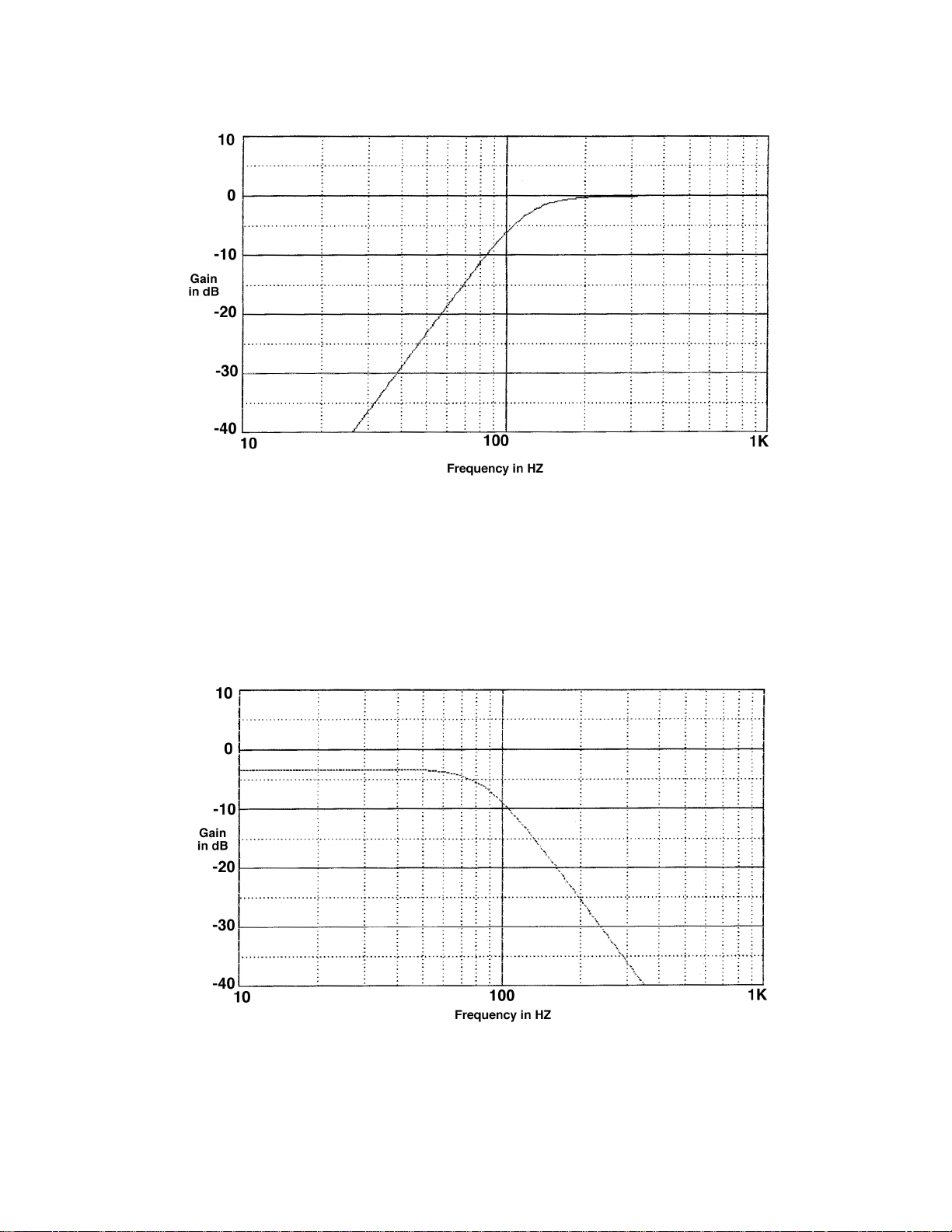
Output is measured from U3 pin 7 or U6 pin 1. Controls are set at:: Mode 4 (Option),
Output Mode: Normal, Low Frequency Level: 0 dB, and Input Level: +4 dB.
Figure 1. High Frequency EQ
Output is measured from U5 pin 14. Controls are set as in Figure 1.
Figure 2. EQA + EQB
5
Page 7
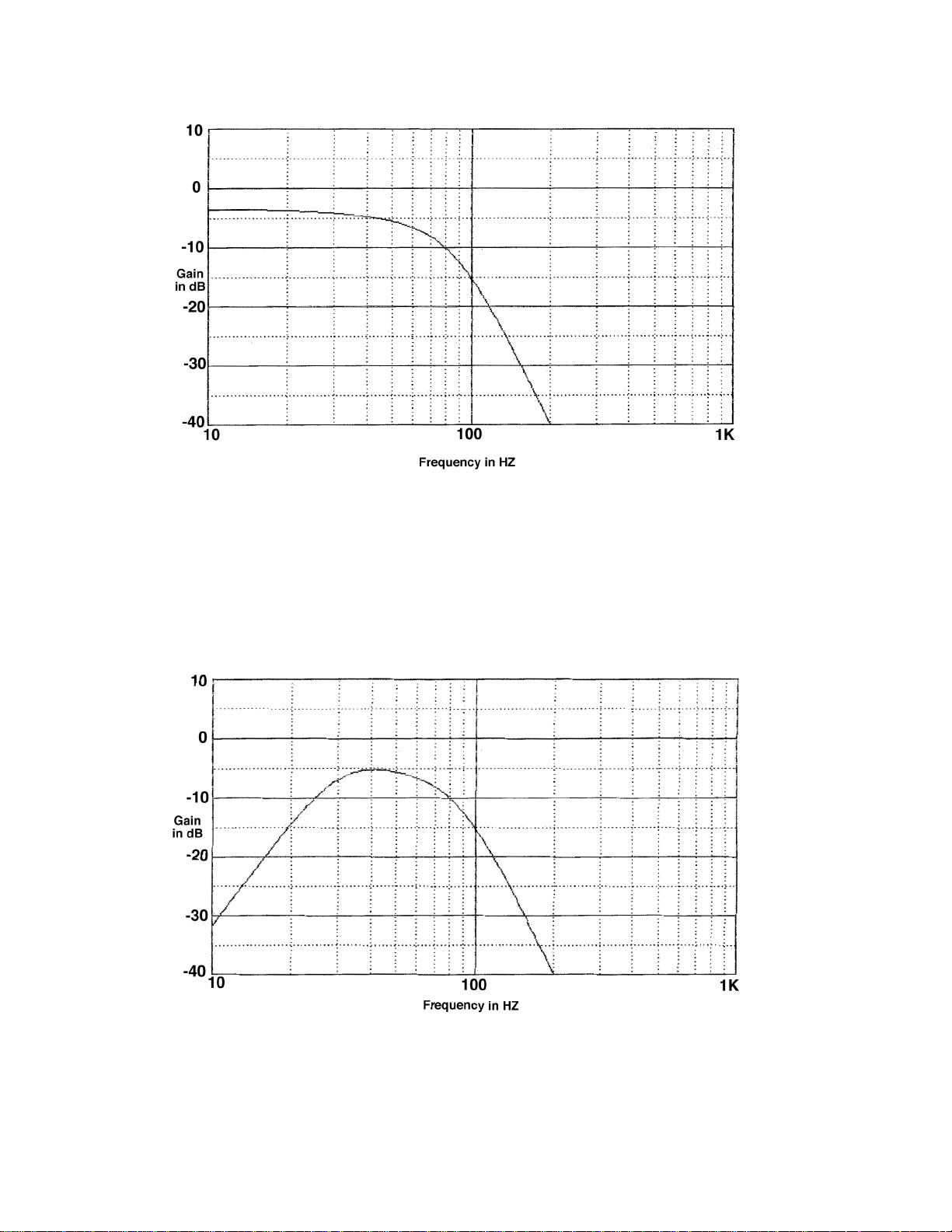
Output is measured from U5 pin 1. Controls are set as in Figure 1.
Figure 3. EQA + EQB + EQC
Output is measured from U5 pin 7. Controls are set as in Figure 1.
Figure 4. EQA + EQB + EQC + EQD
6
Page 8

Output is measured from U3 pin 1. Controls are set as in Figure 1.
Figure 5. EQA + EQB + EQC + EQD + VCA
7
Page 9

Figure 6. OC-1 Block Diagram
8
Page 10

OC-1 Installation Procedures
NOTE: The information included here is to aid
the technician in setting up the OC-1 before
doing any troubleshooting. These procedures
are provided in more depth in the OC-1 Owner's
Guide (P/N 176007).
OC-1 Option Card
Internal Protection
Circuit Harness
External Protection
Circuit Harness
Figure 7. OC-1 Option Card and Harnesses
1. Installing the Internal Protection Circuit
Harness
A. Turn the controller so that its rear panel
faces you. See Figure 8.
B. Remove 4 phillips-head screws.
C. Slide the cover towards you and lift away
from the controller.
D. Find the plastic plug in the controller's
rear panel (Figure 9). Pinch the top lock tab
and push the plug partially out (Figure 9A).
Release the tab and pull the plug completely
out.
9A
Figure 8. Cover and screw removal
Figure 9. Plastic plug removal
9
Page 11

10B
10A
Flat side of barrel
10C
Figure 10. Internal Harness Connection
E. Remove the lock nut and washer from the
harness (Figure 10A).
F. Thread the harness through the rear
panel (white connector first).
G. Turn the barrel connector so that its flat
side matches the flat side of the hole in the
controller. The connector should sit firmly
against the outside of the rear panel (Figure
10B).
H. Replace the lock nut and washer on the
harness inside the rear panel. Tighten firmly
with needle nose pliers (Figure 10C).
2. Connecting the OC-1 to the controller
NOTE: The controller's rear panel should
face you and the internal harness should be
inside.
A. Turn the OC-1 PCB so that its component
side faces you.
B. Connect the harness to J1 on the OC-1
PCB (Figure 11).
C. Plug the PCB into the connector
receptacles located on the controller's PCB.
See Figure 12 for proper orientation.
3. Installing the External Protection Circuit
Harness
A. Attach the external harness to the internal
harness connector (Figure 13) by turning
the notch on the harness to the right.
B. Hand tighten the lock nut on the external
harness.
Figure 11. System Controller Connection
Figure 12. OC-1 connected to controller PCB
10
Page 12

Figure 13. External Harness Connection
C. Connect the harness's other end to the speaker terminals on your amplifier with either screw
lugs (Figure 14A) or a banana plug (Figure 14B). Connect the red wire to the positive (+)
terminal and the black wire to the negative (-) terminal.
NOTE: Figure 15 shows a typical system hookup.
Figure 14A. Screw terminal
Figure 15. Complete system hookup
Figure 14B. Banana plug
11
Page 13

Test Setup
OC-1 Test Procedures
Input Connections: Connect an oscillator to the
positive (+) and negative (-) input terminals for
Channels 1 or 2. These procedures assume that
the person performing these tests is using test
equipment with unbalanced inputs and outputs.
See Figure 16 for connection information. Also,
refer to Figure 15 for a system hookup diagram.
Output Connections: Connect test equipment to
the positive (+) and negative (-) output terminals
for Channels 1 or 2 (low and high frequency
outputs).
All tests should be performed for both
channels.
All test equipment must be isolated from
ground (floated).
See Figure 17 for a picture of the controller's
back panel.
• Output mode switch should be set at
normal
• Input switches should be set at +4 dB
• Low frequency level potentiometer should
be set at 0 dB
**IMPORTANT NOTE**
Install the external protection circuit harness for all
tests. Otherwise, the controller's bass channel (as a
safety measure) will shut down.
1. Frequency Response of High Frequency (HF)
Output
A. Apply a 100 mVrms, 600 Hz signal to the
controllers's input terminals and reference your
dB meter to this frequency.
The controls on the back panel should be set as
follows:
• Mode switch should be set at 4 (Option)
Frequency (Hz) 402™ Controller
Response (dB)
40 -29.2 ± 1.5 dB -23.5 ± 1.5 dB -17.57 ± 1.5 dB
80 -8.3 ± 1.5 dB - 5.6 ± 1.5 dB -1.84 ± 1.5 dB
100 -3.0 ± 1.5 dB +0.8 ± 1 .5 dB +2.0 ± 1.5 dB
120 0 dB +1.6 ± 1 .5 dB +4.0 ± 1.5 dB
150 +1.83 ± 1.5 dB +1.93 ± 1.5 dB +4.7 ± 1.5 dB
180 +2.16 ± 1.5 dB +0.7 ± 1.5 dB +4.2 ± 1.5 dB
200 +2.11 ± 1.5 dB +.15 ± 1.5 dB +3.7 ± 1.5 dB
600 REF REF REF
2200 +2.12 ± 1.5 dB +3.5 ± 1.5 dB +1.61 ± 1.5 dB
5000 +7.5 ± 1.5 dB +12.5 ± 1.5 dB +7.29 ± 1.5 dB
15000 +12.85 ± 1.5 dB +19.0 ± 1.5 dB +17.02 ± 1.5 dB
B. Measure the frequency response across the
HF outputs according to the chart below. This
chart provides responses for the 402, 502, and
802 II controllers (with the option card installed).
502™ Controller
Response (dB)
802® II Controller
Response (dB)
12
Page 14

Input Connections
Audio
Oscillator
Audio
Oscillator
Output Connections
Figure 16. Unbalanced Connections
INPUT LEVEL
–10 +4
SER. NO. D.O.M.
Input
connectors
INPUT
CH 1
Input
attenuator
switches
High frequency
output
connectors
Bass level
control
HIGH FREQ OUTPUT
MODE
INPUT LEVEL
4
3
–10 +4
2
CH 2
PROTECTED BY U.S. PATENT 3,038,964
1
CH 1 CH 2
Mode
switch
LOW FREQ
LEVEL
.
0
.
OUTPUT MODE
.
.
.
.
.
NORM SUM
+3
-18
BOSE CORPORATION, FRAMINGHAM, MA 01701-9168
ENGINEERED AND MANUFACTURED IN U.S.A.
Bass mono
sum switch
Low frequency
output
connectors
LOW FREQ OUTPUT
+– +–+– +–+– +–
CH 1 CH 2
Figure 17. Typical Controller Back Panel (Barrier Strip Version Shown)
13
230V~AC
50/60Hz 12W
LISTED 411F
U
L
®
COMMERCIAL
SOUND
EQUIPMENT
Page 15

2. Frequency Response of LF Output
3. Protection Circuit Test
A. Apply a 100 mVrms, 80 Hz signal to the
controller's input terminals and reference
your dB meter to this frequency.
B. Measure the frequency response across the
LF outputs according to the chart below.
Frequency (Hz) Response (dB)
20 -10.5 ± 1.5
50 +2.25 ± 1.5
80 REF
100 -7.35 ± 1.5
120 -13.68 ± 1.5
150 -21 ± 1.5
180 -27 ± 1.5
200 -30.5 ± 1.5
NOTE: Refer to Figures 13 through 15 and the
installation instructions for connecting the
external protection circuit harness.
A. Connect a signal generator to the controller
input terminals.
B. Connect the controller LF outputs to the
amplifier input terminals.
C. Connect the external protection circuit harness
to the amplifier output.
D. Connect a voltmeter across the amplifier
output terminals.
E. Apply a 57 Hz signal to the controller input
terminals and adjust the signal generator until the
amplifier's output voltage is 40 Vrms.
F. Increase the input to the amplifier until the
output voltage is 47 Vrms. Continue increasing
the input to the amplifier. The amplifier's output
voltage should not rise above 47 volts
(compression occurs at this voltage).
14
Page 16

Notes for Future Reference
15
Page 17

OC-1 Option Card Parts List
OC-1 Packaging Parts List (Figure 16)
Item
Number
1 Cable Assembly 174147 1 1
2 Option Card PCB Assembly 145610 1 2,3
- Bag-Antistatic 174138 1 4
- Card-Owner's Registration 122157 1 4
- Envelope 122785 1 4
- Owner's Manual 176007 1 4
- Carton 145618 N/A 4
1. The cable assembly consists of both the internal and external protection circuit harnesses.
2. This part is not normally available from Customer Service. Approval from the field service
manager is required before ordering.
Description Part Number Qty.
Per
Carton
NOTES
See Note
3. The individual parts located on this PCB are listed in the Electrical Parts List.
4. This part is not illustrated.
16
Page 18

Internal Protection
Circuit Harness
Option Card (2)
External Protection
Circuit Harness
Cable Assembly (1)
Figure 16. Option Card and Cable Assembly
17
Page 19

OC-1 Electrical Parts List
Resistors
Reference
Description Part Number See Note
Designator
R1-4 475 KΩ,1%,1/4W,
52mm,MF
R6,7,41,75,76 7.5 kΩ,1%,
1/10W,0805
R8,39 100 Ω,1%,
1/10W,0805
R9,10,12,14 200 kΩ,5%,
1/10W,0805
R11,17 1 MΩ,5%,1/10W,
0805
R13,90,93 10 kΩ,1%,
1/10W,0805
R15 51 Ω,5%,1/10W,
0805
R16 4.64 kΩ,1%,
1/10W,0805
R18 12.4 kΩ,1%,
1/10W,0805
R19,25,28 20 kΩ,1%,1/10W,
0805
R22 41.2 kΩ,1%,
1/10W,0805
R24 5.1 kΩ,5%,1/10W,
0805
R26,29 7.87 kΩ,1%,
1/10W,0805
R27,30 137 kΩ,1%,
1/10W,0805
R32,37 17.4 kΩ,1%,
1/10W,0805
R33,36 100 kΩ,1%,
1/10W,0805
R34 2.43 kΩ,1%,
1/10W,0805
R35 2.94 kΩ,1%,
1/10W,0805
R38 301 Ω,1%,
1/10W,0805
R45 750 Ω,1%,
1/10W,0805
R48 1.54 kΩ,1%,
1/10W,0805
R50 35.7 kΩ,1%,
1/10W,0805
121245-2214753
133625-7501
133625-1000
133626-2045
133626-1055
133625-1002
133626-5105
133625-4641
133625-1242
133625-2002
133625-4122
133626-5125
133625-7871
133626-1373
133625-1742
133625-1003
133625-2431
133625-2941
133625-3010
133625-7500
133625-1541
133625-3572
18
Page 20

Resistors (Continued)
Reference
Description Part Number See Note
Designator
R52,58,64,65,69,
Jumper-Chip,0805 133627
77,78,83,89,94
R54,62,63 14 kΩ,1%,
133625-1402
1/10W,0805
R85 26.1 kΩ,1%,
133625-2612
1/10W,0805
R88 178 kΩ,1%,
133625-1783
1/10W,0805
R92 1.4 kΩ,1%,1/10W,
133625-1401
0805
R95 255 kΩ,1%,1/10W,
133625-2553
0805
Diodes
Reference
Description Part Number See Note
Designator
D1,4 Zener,5%,18V,1W
116995-4746A
1N4746
D2,3,9 Dual,SOT-23 147239
D5,6 1N4148,75V,
121501
300mA,Switching
or
116997
D7,8 Dual,SOT-23 147249
Integrated Circuits
Reference
Description Part Number See Note
Designator
U1-4,6 Op Amp,RC4559,
Dual
U5 Op Amp-
NJM2059,Quad
U7 VCA, 18V, SIP-8,
2155
Reference
Description Part Number See Note
Designator
J1 Header,2 pos,
Male
J4,5 Header,Rtang,
12 pos.
108568
144008
175120
Connectors
134739-02
149358
19
Page 21

Capacitors
Reference
Description Part Number See Note
Designator
C1,2,57 3300 pF,10%,50V,
X7R,0805
C3 100 µF,20%,25V,
105,Electrolytic
C4,7,13,27,28 10 µF,20%,16V,
105,Electrolytic
C5,6,8,9,18,19,
23-26,38,39,59
.022 µF,10%, 50V,
X7R,0805
C10 22 µF,20%,25V,
BP,EL
C11 1 µF,20%,50V,
105,Electrolytic
C14 100 pF,5%, 50V,
Cog,0805
C15-17,20-22 .047 µF,5%, 63V,
85,Box
C35 .18 µF,5%, 50V,
85,Box
C42 .027 µF,5%, 63V,
85,Box
C43 .47 µF,5%, 50V,
85,Box
C48,51 .22 µF,5%, 50V,
85,Box
C52,54,55 .15 µF,5%, 50V,
85,Box
133623-332
120767
137126-100
133623-223
147522-220
137126-1R0
133622-101
137127-473
137127-184
137127-273
137127-474
137127-224
137127-154
20
Page 22

SPECIFICATIONS AND FEATURES SUBJECT TO CHANGE WITHOUT NOTICE
®
Bose Corporation
The Mountain
Framingham, Massachusetts USA 01701
P/N 174786 6/94: REV.0 FOR TECHNICAL ASSISTANCE OR PARTS ORDERING,CALL 800-367-4008
 Loading...