

Page 1
AM-CL33
SIMPLE-2
Apartofcontentsisadequate.
Re-issuing is under request.
AHK
SERVICE MANUAL
MINIDISC PLAYER
• This Service Manual is the "Revision Publishing" and replaces "Simple Manual"
(S/M Code No. 09-003-430-9T1).
BASIC MD MECHANISM : ZZG-5 B
S/M Code No. 09-007-430-9R2
REVISION
DATA
Page 2

SPECIFICATIONS
Main unit
Playback system MiniDisc digital audio system
Laser pickup Semiconductor laser
Sampling Frequency 44.1 kHz
Number of channels Stereo: 2 channels
D/A converter 1-bit
Frequency response 40 to 20,000 Hz ± 4 dB
Wow and Flutter Below measurable limit
Output Phone jack
Maximum output level 8 mW + 8 mW (16 Ω)
Power requirements DC 1.2 V using the supplied NI-MH
Battery life Using the supplied rechargeable battery
20 to 20,000 Hz ± 1 dB (10 kΩ)
(±0.00 1% W.PEAK)
rechargeable battery MHB-901
DC 1.5 V using an LR6 (size AA) dry
cell battery
AC house current using an optional AC adaptor
Approx. 20 hours (with power save on:
approx. 26 hours)
Using an LR6 (size AA) dry cell battery
Approx. 35 hours (with power save on:
approx. 43 hours)
Using the supplied rechargeable battery and an
LR6 (size AA) dry cell battery
Approx. 60 hours (with power save on:
approx. 70 hours)
Maximum outside Approx. 80 (W) X 20.4 (H) X 82.8 (D) mm
dimensions (31/4 X 13/16 X 33/6 inches) (excluding
Weight Approx. 110 g (3.9 oz) including the
<Battery charger RB-M02 K>
Rated voltage AC 240 V, 50 Hz
• Design and specifications are subject to change without notice.
projected parts and controls)
rechargeable battery.
– 2 –
Page 3
PROTECTION OF EYES FROM LASER BEAM DURING SERVICING
This set employs laser. Therefore, be sure to follow carefully
the instructions below when servicing.
WARNING!!
WHEN SERVICING, DO NOT APPROACH THE LASER
EXIT WITH THE EYE TOO CLOSELY. IN CASE IT IS
NECESSARY TO CONFIRM LASER BEAM EMISSION.
BE SURE TO OBSERVE FROM A DISTANCE OF MORE
THAN 30cm FROM THE SURFACE OF THE OBJECTIVE LENS ON THE OPTICAL PICK-UP BLOCK.
s Caution: Invisible laser radiation when
open and interlocks defeated avoid
exposure to beam.
s Advarsel: Usynlig laserståling ved åbning,
når sikkerhedsafbrydere er ude af funktion.
Undgå udsættelse for stråling.
VAROITUS!
Laiteen Käyttäminen muulla kuin tässä käyttöohjeessa
mainitulla tavalla saataa altistaa käyt-täjän
turvallisuusluokan 1 ylittävälle näkymättömälle
lasersäteilylle.
VARNING!
Om apparaten används på annat sätt än vad som
specificeras i denna bruksanvising, kan användaren
utsättas för osynling laserstrålning, som överskrider
gränsen för laserklass 1.
CAUTION
Use of controls or adjustments or performance of procedures other than those specified herin may result in
hazardous radiation exposure.
ATTENTION
L’utillisation de commandes, réglages ou procédures
autres que ceux spécifiés peut entraîner une dangereuse
exposition aux radiations.
ADVARSEL
Usynlig laserståling ved åbning, når sikkerhedsafbrydereer
ude af funktion. Undgå udsættelse for stråling.
This Compact Disc player is classified as a CLASS 1
LASER product.
The CLASS 1 LASER PRODUCT label is located on the
rear exterior.
CLASS 1 LASER PRODUCT
KLASSE 1 LASER PRODUKT
LUOKAN 1 LASER LAITE
KLASS 1 LASER APPARAT
Precaution to replace Optical block
(KMS-330A)
Body or clothes electrostatic potential could
ruin laser diode in the optical block. Be sure
ground body and workbench, and use care the
clothes do not touch the diode.
1) After the connection, remove solder shown in
right figure.
PICK-UP Assy P.C.B
Solder
– 3 –
Page 4
DISASSEMBLY INSTRUCTIONS
About Disassembling and Reassembling
Service position can be established only by removing the PANEL, BOLT.
1. Removing the PANEL, TOP
(1) Remove the five screws “a”.
(2) Remove the PANEL, TOP.
*1 When re-attaching the PANEL, TOP, the arm should be engaged with the HLDR, CTRG.
2. Removing the PANEL, BOT
(1) Remove the screw “a” and the screw “b” and remove the two screws “c”.
(2) While being careful not to bend the screw of the screw hole, remove the PANEL, BOT.
– 4 –
Page 5
3. Removing the HLDR, BATT and PWB, MAIN
(1) Remove the screw “a” and remove the HLDR, BATT.
(2) Short the PICK-UP short land and remove the three connectors b.
(3) Remove the screw “c” and the three screws “d”, then remove the PWB, MAIN.
*1: Take extra caution when attaching the HOLD SW.
*2: Take extra caution when attaching the BAT-CONTACT. In addition, take extra caution when attaching the OPEN SW that is
located on the rear of the PWB, MAIN.
– 5 –
Page 6
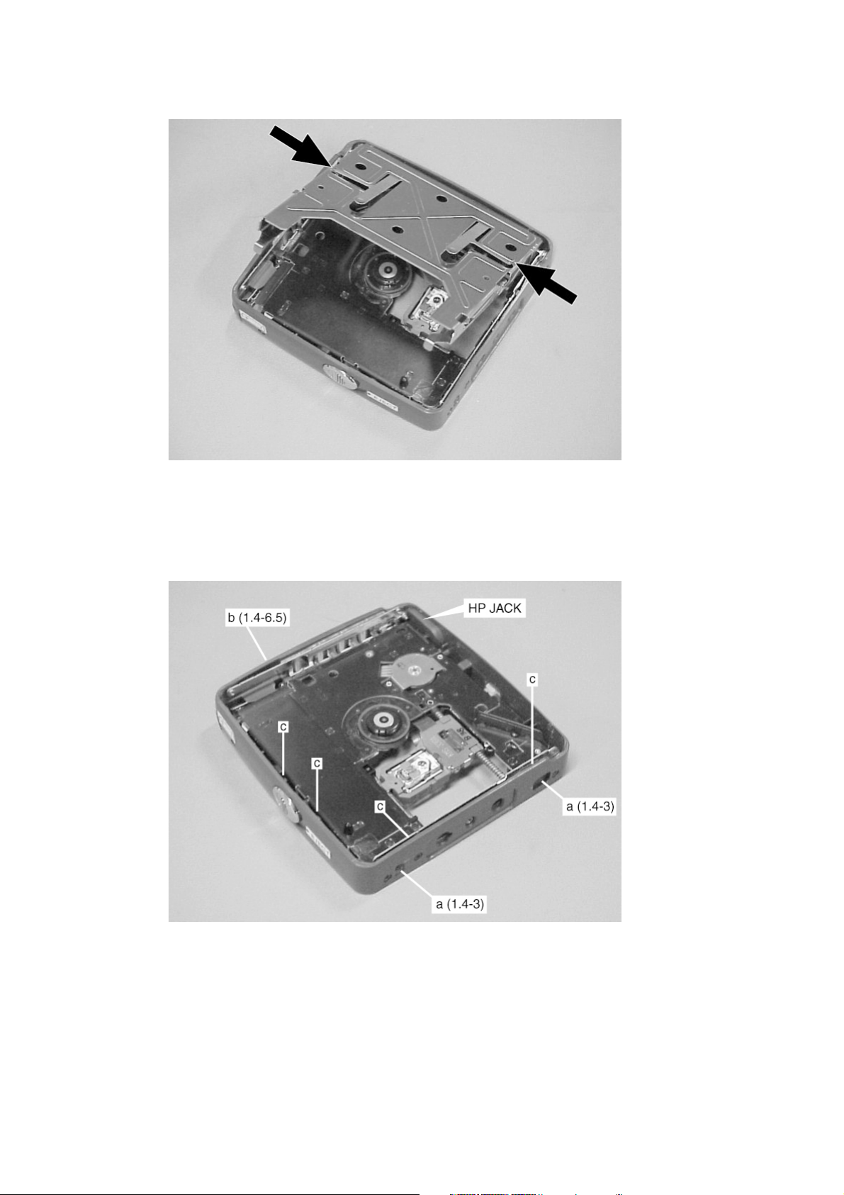
4. Removing the HLDR, CTRG
(1) Bend the HLDR, CTRG in the direction of the arrow shown in the figure and remove the HLDR, CTRG.
5. Removing the mechanism and the FRAME , CENTER
(1) Remove the two screws “a” and remove the screw “b”.
(2) To remove the positioning hole “c” of the mechanism from the FRAME, CENTER, loosen the FRAME, CENTER in the direction
of the arrow and remove the mechanism.
* When attaching them, adjust the position of the HP JACK.
– 6 –
Page 7
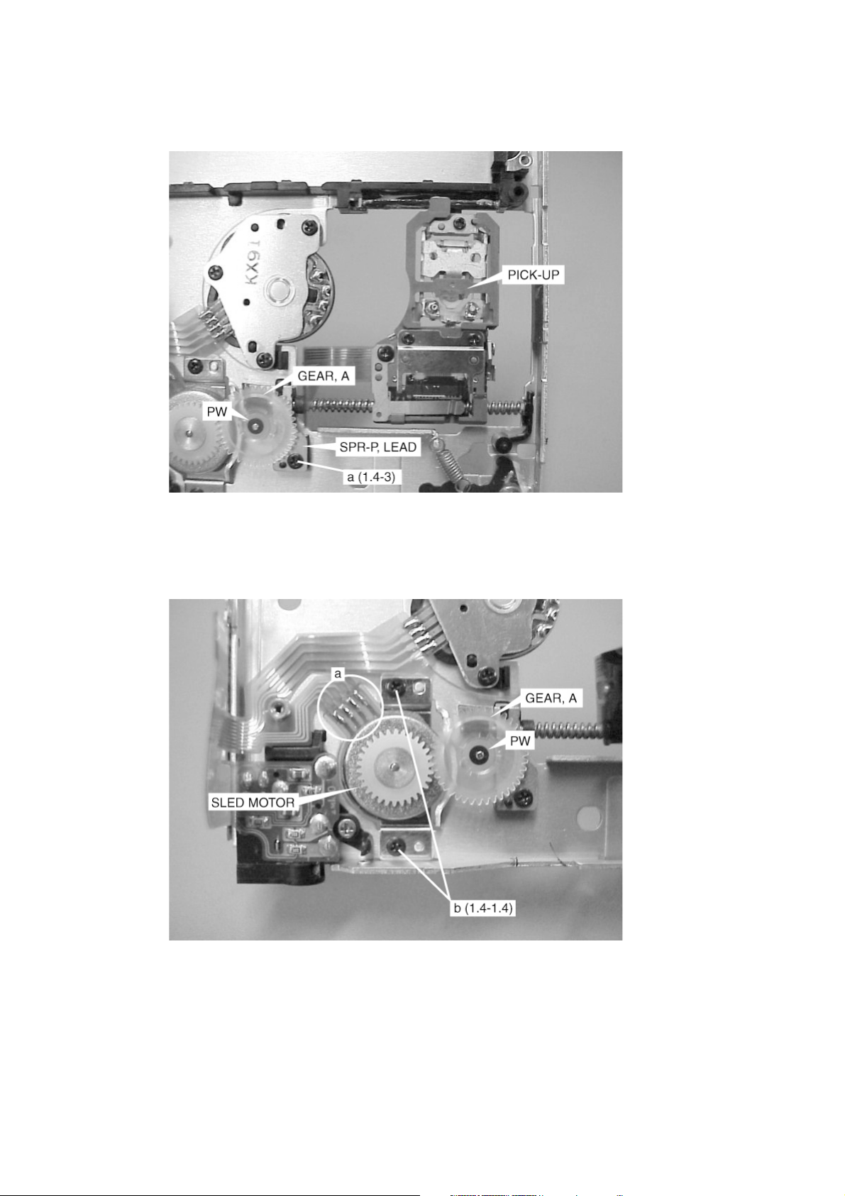
6. Removing the PICK-UP
(1) Remove the poly washer and remove the GEAR, A.
(2) Remove the screw “a” and remove the SPR-P, LEAD.
(3) Remove the shaft and the PICK-UP.
7. Removing the SLD, MOTOR
(1) Remove the poly washer and remove the GEAR, A.
(2) Remove soldering “a”
(3) Remove the two screws and remove the SLED MOTOR.
– 7 –
Page 8
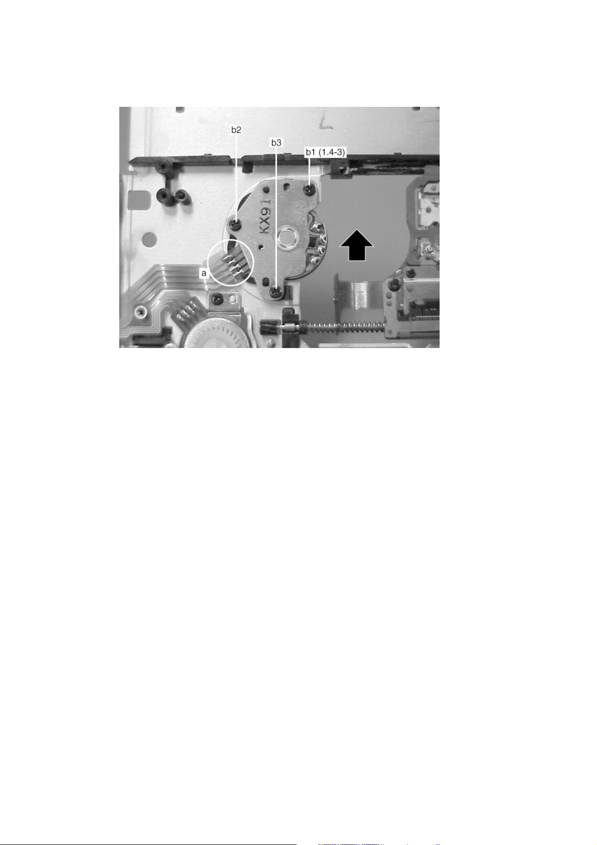
8. Removing the SLED MOTOR.
(1) Remove soldering “a”.
(2) Remove the screws “b1”, “b2” and “b3” and remove the SPINDLE MOTOR.
* To attach the SPINDLE MOTOR, slide it in the direction of the arrow and tighten the screws in order of “b1”, “b2” and “b3”.
– 8 –
Page 9

ELECTRICAL MAIN PARTS LIST
REF. NO.
IC
87-A21-294-010 1H C-IC,LA9606
87-A20-718-040 -- C-IC,TC7S66FU
87-A21-574-010 2Y C-IC,LC89642
87-A21-526-010 2P C-IC,GM71VLS17403CTL-1
87-017-861-040 1B C-IC,TC7W74FU
87-A21-618-040 2P C-IC,TK70006S
8A-HM6-602-010 1B C-IC,LC87F5164(A)
87-A21-030-040 1B C-IC,S-93C46AMFN
87-A21-038-040 2P C-IC,NJU7014R-TE2
87-A21-575-010 1B C-IC,BD6606KVT
87-A21-316-080 1B C-IC,S-8328B24MC
87-A20-861-040 1A C-IC,S-80808ANNP
87-A20-982-040 1A C-IC,S-80822ANNP
87-A21-627-040 1B C-IC,XC6367B102MR
87-A21-341-040 1D C-IC,TA2131FL
TRANSISTOR
87-A30-033-080 0E C-FET,2SK2035
87-A30-149-080 0E C-FET,2SJ347
89-115-884-080 0E C-TR,2SA1588Y
87-A30-181-040 0E C-TR,DTA114TEA
87-A30-180-040 0E C-TR,DTC114TEA
87-A30-261-080 1B C-FET,FDC633N
87-A30-262-080 1B C-FET,FDC634P
89-332-654-080 0E C-TR,2SC3265Y
87-A30-147-080 0E C-TR,2SA1832GR
87-A30-499-040 -- C-FET,2SK2009
DIODE
87-017-850-080 0E C-DIODE,DAP222
87-A40-687-080 0E C-DIODE,M1FH3
MAIN C.B
C101 87-A10-770-080 0E C-CAP,V 0.1-10 K B
C102 87-A10-765-080 0E C-CAP,V 0.033-10 K B
C103 87-A10-766-080 0E C-CAP,V 0.047-10 K B
C104 87-A10-765-080 0E C-CAP,V 0.033-10 K B
C105 87-A10-765-080 0E C-CAP,V 0.033-10 K B
C106 87-A10-765-080 0E C-CAP,V 0.033-10 K B
C107 87-A10-765-080 0E C-CAP,V 0.033-10 K B
C108 87-A10-531-080 0E C-CAP,V 10P-50 D CH
C109 87-A10-523-080 0E C-CAP,V 2.0P-50 C CK
C110 87-A11-058-080 0E C-CAP,U 0.22-10 K B
C111 87-A10-561-080 0E C-CAP,V 0.01-16 K B
C112 87-A10-561-080 0E C-CAP,V 0.01-16 K B
C114 87-A10-770-080 0E C-CAP,V 0.1-10 K B
C115 87-A10-556-080 0E C-CAP,V 2200P-50 K B
C116 87-A11-049-080 0E C-CAP,U 1-6.3 K B
C117 87-A11-751-080 1A C-CAP,TN 22U-4 M P
C118 87-A11-050-080 1A C-CAP,TN 47U-4 M F95 A
C119 87-A10-826-080 1A C-CAP,S 1-10 K B
C120 87-A10-770-080 0E C-CAP,V 0.1-10 K B
C121 87-A11-751-080 1A C-CAP,TN 22U-4 M P
C122 87-A10-561-080 0E C-CAP,V 0.01-16 K B
C123 87-A10-554-080 0E C-CAP,V 1000P-50 K B
C124 87-A10-554-080 0E C-CAP,V 1000P-50 K B
C200 87-016-669-080 0E C-CAP,S 0.1-25 K B
C201 87-A11-050-080 1A C-CAP,TN 47U-4 M F95 A
C202 87-A10-770-080 0E C-CAP,V 0.1-10 K B
C203 87-A10-556-080 0E C-CAP,V 2200P-50 K B
C204 87-A10-671-080 0E C-CAP,V 0.022-16 K B
C206 87-A10-770-080 0E C-CAP,V 0.1-10 K B
C208 87-A10-770-080 0E C-CAP,V 0.1-10 K B
C209 87-A10-770-080 0E C-CAP,V 0.1-10 K B
C212 87-A11-751-080 1A C-CAP,TN 22U-4 M P
C214 87-A10-535-080 0E C-CAP,V 22P-50 J CH
PART NO. DESCRIPTIONREF. NO. KANRI
KANRI
NO.
DESCRIPTION
PART NO.
NO.
C215 87-A10-535-080 0E C-CAP,V 22P-50 J CH
C216 87-A10-770-080 0E C-CAP,V 0.1-10 K B
C217 87-A11-049-080 0E C-CAP,U 1-6.3 K B
C300 87-A11-049-080 0E C-CAP,U 1-6.3 K B
C301 87-A10-561-080 0E C-CAP,V 0.01-16 K B
C302 87-A10-561-080 0E C-CAP,V 0.01-16 K B
C303 87-A10-561-080 0E C-CAP,V 0.01-16 K B
C304 87-A10-561-080 0E C-CAP,V 0.01-16 K B
C305 87-A11-050-080 0E C-CAP,TN 47U-4 M F95 A
C307 87-A10-770-080 0E C-CAP,V 0.1-10 K B
C308 87-A10-770-080 0E C-CAP,V 0.1-10 K B
C309 87-A10-770-080 0E C-CAP,V 0.1-10 K B
C310 87-012-274-080 0E C-CAP,U 1000P-50 K B
C400 87-A11-049-080 0E C-CAP,U 1-6.3 K B
C401 87-A11-049-080 0E C-CAP,U 1-6.3 K B
C402 87-A10-556-080 0E C-CAP,V 2200P-50 K B
C403 87-A10-556-080 0E C-CAP,V 2200P-50 K B
C404 87-A10-556-080 0E C-CAP,V 2200P-50 K B
C405 87-A10-556-080 0E C-CAP,V 2200P-50 K B
C406 87-A10-556-080 0E C-CAP,V 2200P-50 K B
C407 87-A10-556-080 0E C-CAP,V 2200P-50 K B
C408 87-A11-049-080 0E C-CAP,U 1-6.3 K B
C409 87-A10-765-080 0E C-CAP,V 0.033-10 K B
C410 87-A10-765-080 0E C-CAP,V 0.033-10 K B
C411 87-A10-770-080 0E C-CAP,V 0.1-10 K B
C412 87-A10-770-080 0E C-CAP,V 0.1-10 K B
C413 87-A10-770-080 0E C-CAP,V 0.1-10 K B
C414 87-A11-050-080 -- C-CAP,TN 47U-4 M F95 A
C415 87-A11-046-080 1B C-CAP,TN 100U-4 M F95 B
C416 87-A11-751-080 0E C-CAP,TN 22U-4 M P
C417 87-A11-807-080 0E C-CAP,TN 4.7U-6.3 M P
C600 87-A11-806-080 0E C-CAP,TN 47U-6.3 M PSLB
C601 87-A10-557-080 0E C-CAP,V 3300P-25 K B
C602 87-A11-806-080 1B C-CAP,TN 47U-6.3 M PSLB
C603 87-A10-770-080 0E C-CAP,V 0.1-10 K B
C604 87-A10-770-080 0E C-CAP,V 0.1-10 K B
C606 87-A11-807-080 0E C-CAP,TN 4.7U-6.3 M P
C607 87-A11-049-080 0E C-CAP,U 1-6.3 K B
C608 87-A11-751-080 1A C-CAP,TN 22U-4 M P
C609 87-A10-561-080 0E C-CAP,V 0.01-16 K B
C610 87-A10-550-080 0E C-CAP,V 470P-50 K B
C611 87-A11-049-080 0E C-CAP,U 1-6.3 K B
C612 87-A10-561-080 0E C-CAP,V 0.01-16 K B
C613 87-A11-049-080 0E C-CAP,U 1-6.3 K B
C700 87-A11-751-080 1A C-CAP,TN 22U-4 M P
C701 87-A10-770-080 0E C-CAP,V 0.1-10 K B
C702 87-A10-543-080 0E C-CAP,V 100P-50 J CH
C703 87-A10-543-080 0E C-CAP,V 100P-50 J CH
C704 87-A10-543-080 0E C-CAP,V 100P-50 J CH
C705 87-A10-543-080 0E C-CAP,V 100P-50 J CH
C706 87-A11-049-080 0E C-CAP,U 1-6.3 K B
C707 87-016-449-080 1A C-CAP,TN 10-4 M S
C708 87-016-449-080 1A C-CAP,TN 10-4 M S
C709 87-A11-058-080 0E C-CAP,U 0.22-10 K B
C710 87-A11-058-080 0E C-CAP,U 0.22-10 K B
C711 87-A11-049-080 0E C-CAP,U 1-6.3 K B
C712 87-A11-049-080 0E C-CAP,U 1-6.3 K B
C713 87-A11-751-080 1A C-CAP,TN 22U-4 M P
C715 87-A11-318-080 1B C-CAP,TN 220U-2.5 SVB2
C716 87-A11-318-080 1B C-CAP,TN 220U-2.5 SVB2
C717 87-A11-049-080 0E C-CAP,U 1-6.3 K B
C719 87-A11-049-080 0E C-CAP,U 1-6.3 K B
C720 87-A11-058-080 0E C-CAP,U 0.22-10 K B
C800 87-012-274-080 0E C-CAP,U 1000P-50 K B
CN100 87-A61-276-080 1B C-CONN,20P H 545482090
CN300 87-A61-020-080 1A C-CONN,4P H 54550-0417
CN700 87-A60-954-080 1B C-CONN,16P H 54548-1611
D300 87-A40-556-080 0E C-LED,CL-270HR RED
L100 87-A50-360-080 0E C-COIL, 47UH K NLFC252018
L101 87-003-245-080 0E C-COIL,2125 22UH K MLF2012
– 9 –
Page 10
PART NO.
L200 87-003-245-080 0E C-COIL,2125 22UH K MLF2012
L300 87-005-769-080 0E C-COIL,2125 100UH K MLF2012
L400 87-A50-475-080 0E C-COIL, 10UH K NLFC201614
L401 87-A50-475-080 0E C-COIL, 10UH K NLFC201614
L402 87-A50-475-080 0E C-COIL, 10UH K NLFC201614
L403 87-A50-475-080 0E C-COIL, 10UH K NLFC201614
L404 87-A50-537-080 0E C-COIL, 100UH C4-K3L
L405 87-A50-011-080 0E C-COIL, 47UH LQH3C
L406 87-003-245-080 0E C-COIL,2125 22UH K MLF2012
L600 87-A50-537-080 1A C-COIL, 100UH C4-K3L
L601 87-A50-012-080 0E C-COIL, 100UH LQH3C
L701 87-005-769-080 1A C-COIL,2125 100UH K MLF2012
L702 87-A50-233-080 1A C-COIL,ACM4532-102-3P
!
PR600 87-A91-769-080 1A C-PROTECTOR,0.75A ERY32SB075
!
PR601 87-A91-769-080 1A C-PROTECTOR,0.75A ERY32SB075
R305 87-022-239-080 0E C-RES,U 10K-1/16W F
R306 87-022-249-080 0E C-RES,U 27K-1/16W F
R615 87-A00-722-080 0E C-RES,V 33K-1/16W F
R616 87-A00-723-080 0E C-RES,V 56K-1/16W F
R701 87-A50-208-080 0E C-COIL,BLM11A601SPT
NO.
CHIP RESISTOR PART CODE
DESCRIPTIONREF. NO. KANRI
PART NO.
NO.
R702 87-A50-208-080 0E C-COIL,BLM11A601SPT
S300 87-A91-436-080 1A C-SW,PUSH 2-1-1 SPVE3.8
S301 87-A90-703-080 0E C-SW,SL 1-1-3 SSSS813-B-2B
X200 87-A70-207-080 1B C-VIB,16.9344MHZ SSR-B
X300 87-A70-212-080 1B C-VIB,3.00MHZ PBRC-B
FLEX JACK C.B
8A-HM3-601-010 1E PWB,FLEX JACK
C004 87-A10-260-080 0E C-CAP,U 0.1-16 K B
J700 87-A60-682-010 1B JACK,3.5 ST 7P
FLEX KEY C.B
8A-HM3-602-010 1E PWB,FLEX KEY
DESCRIPTIONREF. NO. KANRI
Chip Resistor Part Coding
88
A
Resistor Code
Chip resistor
Wattage Type Tolerance
1/16W 1005 5% CJ
1/16W
1/10W
1/8W
1608
2125
3216
5%
5%
5%
Symbol
CJ
CJ
CJ
Figure
Value of resistor
Form
L
Dimensions (mm)
t
W
0.55
Resistor Code
108
118
128
LW t
1.0 0.5 0.35 104
1.6 0.8 0.45
2 1.25 0.45
3.2
1.6
: A
: A
– 10 –
Page 11

TRANSISTOR ILLUSTRATION
D
D
D
S
C
G
S
2SJ347
2SK2009
2SK2035
D
D
FDC633N
FDC634P
G
B
E
2SA1588
2SA1832
2SC3265
DTA114TEA
DTC114TEA
– 11 –
Page 12

WIRING – 1 (MAIN) <1 / 2>
181920212223242526272829303132
17 16 15 14 13 12 11 10 9 8 7 6 5 4 3 2 1
A
B
C
D
E
F
G
H
I
J
K
L
M
N
O
P
Q
– 12 –
R
S
T
U
Page 13

WIRING – 1 (MAIN) <2 / 2>
A
B
C
D
E
F
G
H
151413121110987654321
16 17 18 19 20 21 22 23 24 25 26 27 28 29 30 31 32
I
J
K
L
M
N
O
P
Q
R
S
T
U
– 13 –
Page 14

SCHEMATIC DIAGRAM – 1 (MAIN)
– 14 –
Page 15

WIRING - 2 (FLEX JACK / FLEX KEY)
123456789101112131415
A
TO/FROM MAIN C.B
CN700
1
16
B FLEX JACK C.B
34
2
1
C2
C3
C1
J701
COM
U
V
W
M401
(SLED MOTOR)
COM
U
V
W
(SPINDLE MOTOR)
M
B
M
C
M402
D
E
F
G
H
I
J
VOL -
SW5
VOL +
SW4
R4
C FLEX KEY C.B
R3
SW3
R2
SW2
R1
4
1
TO/FROM MAIN C.B
CN300
SW1
K
L
M
N
O
P
Q
R
S
T
– 15 –
U
Page 16

IC BLOCK DIAGRAM
– 16 –
Page 17

IC DESCRIPTION
IC, LC875164A
Pin No. Pin Name I/O Description
1 WSEL O Select signal terminal for writing flash memory (Normally L output).
2 WCLK O CLOCK terminal for writing flash memory (Normally L output).
3 WDATA O DATA I/O terminal for writing flash memory (Normally L output).
4 EMP I Electricity reduction interrupt input.
5 INTB I Interrupt request input from L89642.
6 WRQB I Interrupt request input from L89642.
7 ECO I ECO input terminal.
8 RESET I Micom reset.
9 XT1 – Connect to VDD.
10 XT2 – Not used (L Output).
11 VSS1 – Connect to GND.
12, 13 CF1, CF2 – 3[MHz] clock.
14 VDD1 – Connect to VDD.
15 KEY0 I Main unit KEY A/D input.
16 KEY1 I Remote control KEY input.
17 BATT I Battery voltage A/D input.
18 SE I Sledding drive voltage A/D input.
19 NC O Not used (L Output).
20 BEMFU I
21 BEMFV I Motor driver’s comparator output.
22 BEMFW I
23~25 S1~S3 O Sledding control output.
26 LED O Operation LED control signal output (LED ON with H).
27 CE0 O Chip select signal of LC89642.
28 SWDT0 O Serial data output to LC89642.
29 SRDT0 I Serial data input from LC89642.
30 SCLK0 O Serial clock output to LC89642.
31 DATA2 O Serial data output to EEPROM.
32 DATAE I Serial data input from EEPROM.
33 SCLK2 O Serial clock output to EEPROM.
34 CE2 O Chip select signal output of EEPROM.
35 BEEP O BEEP signal output.
36~40 NC O Not used (L Output).
41 SLPWM O PWM output for VM control of motor driver.
42 VDD2 – Connect to VDD.
43 VSS2 – Connect to GND.
44 KEY0 I Standby cancel signal input by the main unit KEY.
45 KEY1 I Standby cancel signal input by remote control KEY.
46 FOK I FOK signal input
47 VP I VP (CLV servo lock check) signal input.
48 MON3 I Monitor 3 signal input from LC89642.
49 MON2 I Monitor 2 signal input from LC89642.
– 17 –
Page 18

Pin No. Pin Name I/O Description
50 MON1 I Monitor 1 signal input from LC89642.
51 MON0 I Monitor 0 signal input from LC89642.
52 DEFECT I DEFECT signal input.
53 PPIT I PPIT signal input.
54 READ O Output H when reading data.
55 PLG-1 I Insertion detection signal input of head phone jack (L: Inserted).
56 RESET O LC89642 reset signal output.
57 HOLDER I Holder OPEN(H)/CLOSE (L) signal input & standby release.
58 DRAMSW O Power supply control output of DRAM L: (Turn on the power supply of DRAM).
59 PCK I PCK signal input of LC89642.
60 FSEQ I FSEQ signal input of LC89642.
61~63 NC O Not used (L Output).
64 STALL O Power supply control output of BD6606 (H: ON).
65 SHOCK I SHOCK input of LC89642
66,67 NC O Not used (L Output).
68 VSS3 – Connect to GND.
69 VDD3 – Connect to VDD.
70 MCAS O CAS signal output to DRAM.
71 MRAS O RAS signal output to DRAM.
72 BUP O Micom control of DRAM/DSP control switch signal output (H: Micom control).
73 P-CON O System power supply control (L: Turn on the power supply).
74 AMUTE O AUDIO MUTE signal output (H: Turn ON MUTE).
75 RMCDT O Serial data output to liquid crystal remote controller.
76 PWSTB O Standby signal output of headphone driver (L: standby).
77 HOLD I HOLD signal input (L: HOLD ON)
78 SEDIR I Direction input of sledding move (H: inside → outside, L: outside → inside).
79 JAPAN I Domestic / Overseas version switch input (H: Domestic).
80 TEST I Test mode / Main mode switch input (L: Test mode).
– 18 –
Page 19

IC, LC89642
Pin No. Pin Name I/O Description
1 FR I Bias resistance terminal of VCEC oscillation frequency.
2 ISET I Bias resistance terminal of VCEC electric current charging pump.
3 VCVDD – Power supply terminal for VCEC.
4 PDO O Electric current charging pump output terminal of VCEC.
5 TEST3 I Test input terminal.
6 TEST2 I Test input terminal.
7 SLCO O Slice level output terminal of HF signal.
8 SLCIST I Bias resistance terminal of slice level adjustment amplifier.
9 EFMIN I HF signal input terminal.
10 RESETB I System Reset.
11 TEST1 I Test input terminal.
12 HFL I Track detection signal input terminal.
13 VDD2 – Power supply terminal.
14 VSS – Ground terminal.
15 VDD1 – Internal power supply terminal.
16 AVSS1 – Ground terminal for digital servo.
17 PEAK I PEAK signal input terminal.
18 BOTTOM I BOTTOM signal input terminal.
19 ABCD I Main beam light amount signal input terminal.
20 TE I Tracking error signal input.
21 FE I Focus error signal input terminal.
22 VC I Intermediate electric potential input terminal.
23 AVDD1 – Power supply terminal for digital servo.
24 MAD9 O Address output terminal to DRAM (Not connected).
25 DSW1 O Disc mode switch output.
26 MAD8 O Address output terminal to DRAM (Not connected).
27 DSW0 O Disc mode switch output.
28 MAD7 O Address output terminal to DRAM (Not connected).
29 SGC O AGC control signal output terminal.
30 MAD6 O Address output terminal to DRAM (Not connected).
31 AOFFSET O ABCD offset control signal output terminal.
32 MAD5 O Address output terminal to DRAM (Not connected).
33 FOFFSET O Focus offset control signal output terminal.
34 TOFFSET O Tracking offset control signal output terminal.
35 MAD4 O Address output signal to DRAM (Not connected).
36 TBAL O Tracking balance control signal output terminal.
37 LDREF O Laser control signal output.
38 FBAL O Focus balance control signal output.
39 VDD1 – Internal power supply.
40 VSS – GND.
41 VDD2 – Power supply.
42 MAD3 – DRAM address output.
– 19 –
Page 20

Pin No. Pin Name I/O Description
43 SPPWMF O Spindle PWM output.
44 SPPWMR O Spindle PWM output.
45 SLPWMF O Sled PWM output.
46 MAD2 O DRAM address output.
47 SLPWMR O Sled PWM output.
48 MAD1 O DRAM address output.
49 FOPWMF O Focus PWM output.
50 MAD0 O DRAM address output.
51 FOPWMR O Focus PWM output.
52 TRPWMF O Tracking PWM output.
53 TRPWMR O Tracking PWM output.
54 MAD10 O DRAM address output.
55 AVDD - 1bit D/C converter power supply.
56 OUTL O 1bit D/C converter left channel output.
57 OUTR O 1bit D/C converter Right channel output.
58 AVSS O 1bit D/C converter ground.
59 VDD2 – Power supply.
60 XIN I 16.9344MHz oscillator circuit input.
61 XOUT O 16.9344MHz oscillator circuit input.
62 VSS – GND.
63 VDD1 – Power supply.
64 F16M I 16.9344MHz circuit input.
65 ENH O De-emphasis indicator output.
66 LRCO O LR clock output.
67 DDATA O Expanded audio data output.
68 BCO O Bit clock output.
69 DDOUT O Digital audio output.
70 SMON3 O Monitor signal output.
71 SMON2 O Monitor signal output.
72 SMON1 O Monitor signal output.
73 SMON0 O Monitor signal output.
74 FSEQ O Frame period detection signal output.
75 VP O CLV servo lock recognition output.
76 MRASBT O Test output terminal.
77 MRASB O RAS signal output terminal to DRAM (Not connected).
78 FOK O Focus OK signal output terminal.
79 MWEB O WE signal output terminal to DRAM (Not connected).
80 DEFECT O Defect signal input and output terminal.
81 MD1 I/O Data input and output terminal to DRAM (Not connected).
82 FG I Speed pulse input terminal.
83 CL I Data transfer clock input terminal for CPU interface.
84 CE I Chip enable signal input terminal for CPU interface.
– 20 –
Page 21

Pin No. Pin Name I/O Description
85 MD0 I/O Data input and output signal output terminal to DRAM (Not connected).
86 DI I Data input terminal for CPU interface.
87 VDD1 – Internal power supply terminal.
88 DO O Data output terminal for CPU interface.
89 VDD2 – Power supply terminal.
90 VSS – Ground terminal.
91 MD3 I/O Data input and output signal output terminal to DRAM (Not connected).
92 WRQB O Interrupt signal output terminal for CPU interface.
93 INTB O Interrupt signal output terminal for CPU interface.
94 ADIPWO I Wobble signal input terminal.
95 MD2 I/O Data input and output signal output terminal to DRAM (Not connected).
96 SHOCK O SHOCK / RFNG output terminal.
97 MCASB O CAS signal output terminal to DRAM (Not connected).
98 PCK O VCEC system clock signal output terminal.
99 MOEB O OE signal output terminal to DRAM (Not connected).
100 VCVSS – Ground terminal for VCEC.
– 21 –
Page 22

IC, BD6606KVT
Pin No. Pin Name I/O Description
1 SPWIN I SPIN detection comparator input (Phase W).
2 SPCOM I SPIN motor coil mid-point input terminal.
3 EXTCLK I Synchronized clock input terminal.
4 C1P – CHARGEPUMP capacitor 1 conne ct terminal +.
5 C1M – CHARGEPUMP capacitor 1 connect terminal -.
6 C2P – CHARGEPUMP capacitor 2 connect terminal +.
7 C2M – CHARGEPUMP capacitor 2 connect terminal -.
8 VG O CHARGEPUMP output.
9 SLVM1 – Stepping power part power supply 1.
10 SLUOUT O Stepping motor output (Phase U).
11 SLPG1 – Stepping power part GND 1.
12 SLVOUT O Stepping motor output (Phase V).
13 SLVM2 – Stepping power part power supply 2.
14 SLWOUT O Stepping motor output (Phase W).
15 SLPG2 – Stepping power part GND 2.
16 SLCOM I STEP motor coil mid-point input terminal.
17 BEMFW O STEP detection comparator output (Phase W).
18 BEMFV O STEP detection comparator output (Phase V).
19 BEMFU O STEP detection comparator output (Phase U).
20 S3 I Stepping decoder input 3.
21 S2 I Stepping decoder input 2.
22 S1 I Stepping decoder input 1.
23 SGND – Small signal part GND (MOS).
24 ASGND – Small signal part GND (Bip.).
25 STHB O H1 and H2 bridge mute terminal.
26 STALL I Standby terminal.
27 PW1VM – Half bridge 1 power part power supply.
28 PW1OUT O Half bridge 1 output.
29 PWPG – Half bridge power part GND.
30 PW2VOUT – Half bridge 2 output.
31 PW2VM – Half bridge 2 power part power supply.
32 PWIN2 I Half bridge 2 input.
33 PWIN1 I Half bridge 1 input.
34 IN2R I H bridge 2 reverse input.
35 IN2F I H bridge 2 forward input
36 IN1R I H bridge 1 reverse input.
37 IN1F I H bridge 1 forward input.
38 H2PG2 – H bridge 2 power part GND2.
39 H2ROUT O H bridge 2 reverse output.
40 H2VM – H bridge 2 power part power supply.
41 H2FOUT O H bridge 2 forward output.
42 H2PGI – H bridge 2 power part GND1.
– 22 –
Page 23

Pin No. Pin Name I/O Description
43 H1PG2 – H bridge 1 power part GND2.
44 H1ROUT O H bridge 1 reverse output.
45 H1VM – H bridge 1 power part power supply.
46 H1FOUT O H bridge 1 forward output.
47 H1PG1 – H bridge 1 power part GND1.
48 CST – Start oscillation capacitor connection terminal.
49 CSL1 – Slope capacitor connection terminal 1.
50 CSL2 – Slope capacitor connection terminal 2.
51 FG O FG output.
52 BRK- I Break comparator input (–).
53 BRK+ I Break comparator input (+).
54 VCC2 – Small signal part power supply terminal 2(Bip.).
55 VCC1 – Small signal part power supply terminal 1(MOS).
56 SPVM1 – Spindle power part power supply 1.
57 SPUOUT O Spindle motor output (Phase U).
58 SPPG1 – Spindle power part GND 1.
59 SPVOUT O Spindle motor output (Phase V).
60 SPVM2 – Spindle power part power supply 2.
61 SPWOUT O Spindle motor output (Phase W).
62 SPPG2 – Spindle power part GND 2.
63 SPUIN I SPIN detection comparator input (Phase U).
64 SPVIN I SPIN detection comparator input (Phase V).
– 23 –
Page 24

IC, LA9606
Pin No. Pin Name I/O Description
1 PPIT O Pit / Group identification signal output. Hi=pit, Lo=group
2 VCC –- Power supply pin of Matrix system.
3 J I Photo diode connection pin of pickup. Form RF signal with I pin.
4 I I Photo diode connection pin of pickup. Form RF signal with J pin.
5 P I Photo diode connection pin of pickup. Form TE signal with E pin.
6 E I Photo diode connection pin of pickup. Form TE signal with F pin.
7DI
8CI
9BI
10 A I
11 VEE – Ground pin of Matrix system.
12 NC – Not used.
13 LDD O APC circuit output pin.
14 NC – Not used.
15 LDS I APC circuit input pin.
16 LDREF I Input pin for laser power setting.
17 TBAL I EF balance adjustment pin.
18 TOFF I Offset adjustment pin of TE signal.
19 FOFF I Offset adjustment pin of FE signal.
20 AOFF I Offset adjustment pin of ABCD signal.
21 SGC I VCA gain control pin.
22 DSW0 I
23 DSW1 I
Photo diode connection pin of pickup. It forms FE signal, ABCD signal, and WOO signal
Disc mode setting pin. Hi = Disc with low reflectance, Lo = Disc with high reflectance. Laser
OFF when DSW0 and DSW1 are in Lo.
Disc mode setting pin. Hi = Track in pin line, Lo = Track in group. Laser OFF when DSW0 and
DSW1 are in Lo.
24 NC – Not used.
25 VR – Pass-con connection pin for 1/2VCC.
26 VC O 1/2VCC output pin.
27 FE O Focus error signal output pin.
28 TE O Tracking error signal output pin.
29 ABCD O Main beam light amount signal output pin.
30 HFLIN I HEL signal forming pin in group mode.
31 NC – Not used.
32 BOTTOM O Bottom signal output pin of RF signal.
33 PEAK O Peak signal output pin of RF signal.
34 HFL O HFL signal (Track ON/OFF) output pin
35 RFVEE – Ground pin of RF system
36 EQO O RF equalizer output pin
37 EQI I RF equalizer input pin.
38 RFO O RF signal output pin.
39 CHFL – Capacitor connection pin for bottom hold.
40 RFVCC – Power supply pin of RF system.
– 24 –
Page 25

Pin No. Pin Name I/O Description
41 ADIPCR O ADIP carrier signal output pin.
42 NC – Not used.
43 WOO O Wobble signal output pin.
44 WOI I Wobble signal input pin.
45 SETR I Band pass filter setting pin.
46 CAD – Capacitor connection pin of wobble signal for DC cut.
47 BWCT I Band pass filter switch pin of wobble signal.
48 SLEEP I Sleep mode. SLEEP=Hi: Power ON, SLEEP=Lo: Power OFF.
– 25 –
Page 26

TEST MODE
The operations are displayed by LCD of the remote controller.
The keys of the main unit and remote controller can control shifts between operations.
* TEST MODE will ignore any abnormalities during operations. Plug off the power supply once any abnormalities are detected.
* HOLD switch of the remote controller will function in TEST MODE.
TEST MODE
1. How to activate and cancel Test Mode
(1) How to activate
Turn ON the power supply (set batteries) while pressing "VOL-" keys of the both main unit and remote controller.
Once Test Mode is activated, LCD will all light up and EL backlight will be turned ON.
Then it displays "Engineer MODE".
(2) How to cancel
Turn OFF the power supply to cancel Test Mode.
LCD Display when Test Mode is activated.
2. TEST MODE operations
There are 0~13 Test Modes, which are in the order of playback operations. These modes may be selected using VOL+/- keys, while they can be
started or stopped by pressing PLAY key. If a Test Mode is selected, a data will be displayed in "$XXXX".
* The values displayed in "$XXXX" are just IC internal data and their numerical values are of no significance (except for that of No.0, 13)
If any abnormalities were detected during the operation, it displays "Failed".
No. LCD Display Contents
0 00 050c Xe ALL SV ON (EEPROM Data)
1 01 VC $XXXX VC offset
2 02 ABCD $XXXX ABCD input offset
3 03 FE $XXXX Focus Error offset
4 04 TE $XXXX Tracking Error offset
5 05 FOCUS CHK Focus search(Focus servo OFF)
Spindle Rough Servo
6 06 FOCUS SRCH Focus search, Spindle rough servo
FOCUS ON! Focus servo ON during DISC IN
7 07 Laser $XX Laser power adjustment value
8 08 ABCD G $XX ABCD AGC
9 09 EF $XXXX Traverse adjustment value
10 0A FG $XXXX Focus Gain adjustment value
11 0B TG $XXXX Tracking Gain adjustment value
12 0C FB $XXXX Focus Bias adjustment value
13 0D 050c Xe ALL SERVO ON(Operate all of 1-12)
– 26 –
Page 27

(1) Checking Laser Power
The display will repeat the string of OFF-> PIT Laser Power -> GRV Laser Power -> OFF every time DISP/SEARCH key of the remote
controller is pressed.
* Laser will not be luminescent.
• LCD Display
PIT Laser Power "LDPP $XX"
GRV Laser Power "LDPG $XX"
(2) Checking Sled Operation
Sled operation can be checked between Mode No. 0, 5~12.
Press F-SKIP to shift the pick-up towards the external circumference.
Press B-SKIP to shift the pick-up towards the internal circumference.
(3) Checking Switch Operation
OPEN/CLOSE SW and HOLD SW on a disc holder can be checked on LCD of the remote controller.
• Light up when the disc holder is closed.
• Alarm mark will light up when HOLD SW on the main unit is turned ON. While POWER SAVE is on, "–" will light up.
It does not display HOLD SW of the remote controller.
HOLD SW
OPEN/CLOSE SW
– 27 –
Page 28

ADJUSTMENT MODE
1. How to activate and cancel Adjustment Mode
Operations in Adjustment Mode can be checked on the LCD of the remote controller.
TP1
IC300
IC200
TP4
TP5
TP3
(RF)
TP2
(VC)
MAIN circuit board Test Points
(1) How to activate
Turn ON the power (set batteries) while shorting TP1 of the main circuit board. Once Adjustment Mode is activated,
LCD will all light up and EL backlight will be turned ON.
Then it displays "Manufacture MODE".
Press "PLAY/STOP" key twice to display "IDLE".
(2) How to cancel
Turn OFF the power supply to cancel Adjustment Mode.
(3) Disc to be used
PIT disc (pre-mastered disc): TEST DISC (TGYS1)
GRV disc (MO disc): SONY MDW-74 (fully recorded)
– 28 –
Page 29

(4) Note
• If a disc had any stains or scars on, the adjustment may not be completed.
• Always place the main unit with its cassette cover upward for adjustment.
• Do not make any manual adjustments.
• If the adjustment is incomplete, it displays "NO ADJ" during normal operation.
(5) Prohibitions
Do not press DSL key of the remote controller. If it was pressed, the mode will change to factory shipment mode.
If any data is changed in this mode, the unit will not be able to function normally.
If accidentally change into this mode, initialize EEPROM and re-do all the adjustments.
2. Adjustment Procedures
(1) PIT Disc (TEST DISC: TGYS1)
Insert the disc and press "PLAY" key (make sure to place main unit with its cassette cover upward).
LCD of the remote controller will be displayed "AUTO ADJ H" first, then "COMPLEAT"
(2) GRV DISC (SONY MDW-74)
Insert the disc and press "PLAY" key (make sure to place main unit with its cassette cover upward).
LCD of the remote controller will be displayed "AUTO ADJ L" first, then "COMPLEAT"
* If it displayed "Failed" during adjustment, it means that some abnormalities are deteced and the operation is
terminated.
(3) Checking RF Level and Error Rate
a)Press "–" key of the remote controller. Display "032c 00e" and playback.
Check the RF waveform (TP3) with an oscilloscope and it is within the 1.0±0.2Vp-p. If it
is not, follow the instruction below to make an adjustment.
• If the value is higher than 1.2Vp-p, short TP4.
• If the value is lower than 0.8Vp-p, short TP5.
b) Press "+" of the remote controller. Display "600c 00e" and playback.
Make sure if the error note is below "60e".
3. Others
(1) EEPROM Initialization
Press "DISPLAY" key, while it displays "IDLE", to start initialization of EEPROM.
Once the initialization is completed, LCD displays "EP INIT OK".
• Re-adjustments are required after every initialization. Otherwise it displaysÅuNO ADJUST!Åvduring the normal
operation.
(2) Checking Sled Operation
Press "F-SKIP" key, while it displays "IDLE", to shift puck-up towards the external circumference.
Press "B-SKIP" key, while it displays "IDLE", to shift puck-up towards the internal circumference.
– 29 –
Page 30

MECHANICAL EXPLODED VIEW 1 / 1
B
b
2
B
1
B
B
B
10
11
3
P.C.B
ZZG-5
5
a
F
13
P.C.B
A
F
9
7
D
E
15
D
6
A
8
G
b
16
a
B
4
J101
I
P.C.B
17
18
C
C
12
14
– 30 –
C
C
B
C
19
Page 31

MECHANICAL PARTS LIST 1 / 1
PART NO.
NO.
1 8A-HM6-001-010 1D PANEL,TOP<L,AHK1L>
1 8A-HM6-010-010 -- PANEL,TOP LM<LM>
1 8A-HM6-009-010 1C PANEL,TOP P<P,AHK1P>
1 8A-HM6-011-010 1E PANEL,TOP Y<Y>
2 8A-HM3-205-110 1B FRAME ASSY,L
3 8Z-ZG5-213-110 1C HLDR,CTRG
4 8A-HM3-201-210 1C FRAME ASSY,R
5 8A-HM6-205-010 0E HLDR,BATT
6 8A-HM3-215-110 0E BAT-CONTACT, 7 8A-HM3-214-010 0E BAT-CONTACT,+
8 8A-HM3-216-010 0E BAT-CONTACT,EX
9 8A-HM6-004-010 0E KEY,CONT MAIN
10 8A-HM6-005-010 0E LID,BATT
11 8A-HM3-210-010 1A HINGE ASSY,BATT
12 8A-HM3-213-010 0E SHAFT,HINGE BATT
13 87-078-053-010 0E W-P 0.7-2.5-0.28 SLIT
14 8A-HM6-006-010 1B KNOB,SL SL EJECT
15 8Z-HM4-230-010 0E SPR-E,EJECT
16 8A-HM6-201-010 0E HLDR,EJECT
17 8A-HM6-007-010 0E KNOB,SL HOLD
18 8A-HM6-003-010 1A FRAME,CENTER
19 8A-HM6-002-010 1C PANEL,BOT<L>
19 8A-HM6-008-010 -- PANEL,BOT HK L<AHK1L>
19 8A-HM6-015-010 -- PANEL,BOT HK P<AHK1P>
19 8A-HM6-013-010 1B PANEL,BOT LM<LM>
19 8A-HM6-012-010 -- PANEL,BOT P<P>
19 8A-HM6-014-010 -- PANEL,BOT Y<Y>
A 87-078-186-010 0E SCRW-SR,1.4-1.8 CR L
B 87-HM1-243-010 0E S-SCREW,1.4-1.4CRNL
C 87-067-596-010 0E SCREW,V+1.4-3
D 87-078-187-010 0E SCRW-SR,1.4-4.5 CR L
E 8A-HM6-204-010 0E S-SCREW,+1.4-6.5 CR
F 8A-HM3-222-010 0E S-SCREW,+1.4-3.0 CR
G 8A-HM6-208-010 0E S-SCREW,+1.4-5.5 CR
H 8A-HM3-233-010 0E S-SCREW,+1.4-3.5
DESCRIPTIONREF. NO. KANRI
COLOR NAME TABLE
Basic color symbol Color Basic color symbol Color Basic color symbol Color
B Black C Cream D Orange
G Green H Gray L Blue
LT Transparent Blue N Gold P Pink
R Red S Silver ST Titan Silver
T Brown V Violet W White
WT Transparent White Y Yellow YT Transparent Yellow
LM Metallic Blue LL Light Blue GT Transparent Green
LD Dark Blue DT Transparent Orange GM Metallic Green
YM Metallic Yellow DM Metallic Orange PT Transparent Pink
– 31 –
Page 32

MD MECHANISM EXPLODED VIEW 1 / 2 (ZZG-5 B)
1
2
C
10
A
ZZS-2
B
CUSH-R
4
5
A
6
3
7
8
D
9
MD MECHANISM PARTS LIST 1 / 2 (ZZG-5 B)
PART NO.
NO.
1 8Z-ZG5-201-610 1E CHAS ASSY,MECHA
2 8Z-ZG5-208-010 0E GEAR,A
3 8Z-ZG5-207-010 0E SPR-E,EJECT
4 8Z-ZG5-212-010 0E SPR-P,LEAD
5 8Z-ZG5-209-110 0E GEAR,B
6 8Z-ZG5-217-010 0E BRG, 1.1-2-2
7 8Z-ZG5-210-110 1B SHAFT,LEAD
8 87-A91-718-010 2E PICKUP,KMS-330A
9 8Z-ZG5-219-010 0E SPR-P,RACK 2
10 87-A91-488-010 2P MOT,MX-2263
A 88-ZG6-224-010 0E S-SCREW,VBT+1.4-3
B 87-067-393-010 0E SCREW +1.4-1.4
C 87-067-569-010 0E POLY WASHER 0.83-2.5-0.25
D 8Z-ZG5-223-010 0E S-SCREW,VBT+1.4-2
DESCRIPTIONREF. NO. KANRI
– 32 –
Page 33

MD MECHANISM EXPLODED VIEW 2 / 2 (ZZS-2 A)
1
2
P.C.B
3
4
5
6
MD MECHANISM PARTS LIST 2 / 2 (ZZS-2 A)
PART NO.
NO.
1 8Z-ZS2-214-010 0E PLATE,BASE ZZS2
2 8Z-ZS2-204-010 1C BRG ASSY,ZZS2
3 8Z-ZS2-201-010 1C COIL ASSY,ZZS2
4 8Z-ZS2-213-010 1A MAGNET,ZZS2
5 8Z-ZS2-208-010 1C ROTOR ASSY,ZZS2
6 8Z-ZS2-212-010 0E GEAR,ZZS2
DESCRIPTIONREF. NO. KANRI
– 33 –
Page 34

ACCESSORIES / PACKAGE LIST
PART NO.
NO.
1 8A-HM6-902-010 1B IB,HK (ECA)S<AHK1L,AHK1P>
1 8A-HM6-908-010 1A IB,D<Y,LM,L,P>
2 87-B30-066-210 2B CHARGER,RB-M01<Y,LM,L,P>
2 87-B30-244-010 2P CHARGER,RB-M02K<AHK1L,AHK1P>
3 87-B30-221-010 1B CASE,BATTERY
4 87-B30-295-010 -- HEADPHONE,HP-M031 S<Y,LM,P,AHK1P>
4 87-B30-372-010 2M HEADPHONE,HP-M030 L1<L,AHK1L>
5 87-B30-303-010 2P BAT,MHB-901 (S)
6 8A-HM3-951-010 1F BOX,BAT ASSY AHM-3<Y,LM>
6 8A-HM3-953-010 1F BOX,BAT ASSY AHM-3 P<P,AHK1P>
6 8A-HM3-952-010 1F BOX,BAT ASSY AHM-6 L<L,AHK1L>
7 8A-HM6-951-010 2Y BAG CARRYING
8 8A-HM6-953-010 2B RC UNIT,RC-CL33 L<L,AHK1L>
8 8A-HM6-955-010 2B RC UNIT,RC-CL33 P<P,AHK1P>
8 8A-HM6-956-010 2B RC UNIT,RC-CL33 LM<LM>
8 8A-HM6-957-010 2B RC UNIT,RC-CL33 Y<Y>
9 8A-HM6-954-010 -- CLIP,RC-CL33
DESCRIPTIONREF. NO. KANRI
– 34 –
Page 35

2–11, IKENOHATA 1–CHOME, TAITO-KU, TOKYO 110, JAPAN TEL:03 (3827) 3111
Printed in Singapore9620450 0251431
 Loading...