

Page 1

Table of Contents
Note: This service manual has been updated with information from service manual supplement
175032-S2. This supplement affects part number for R146 and R246 as used on the amplifier PCB.
Refer to 175032-S2 for more information.
SAFETY INFORMATION...................................................................................................... 2
ELECTROSTATIC DISCHARGE SENSITIVE (ESDS) DEVICE HANDLING....................... 3
SPECIFICATIONS ................................................................................................................4
Figure 1. Bass Channel Frequency Response Curve ................................................ 5
Figure 2. Left/Right Channel Frequency Response Curve ........................................5
Figure 3. AM-3P II Amplifier PCB Assembly Block Diagram...................................... 6
Figure 4. AM-3P II Equalizer PCB Assembly Block Diagram ..................................... 6
AM-3P II THEORY OF OPERATION .................................................................................... 7
AM-3P II DISASSEMBLY/ ASSEMBLY PROCEDURES ................................................... 13
AM-3P II TEST PROCEDURES ......................................................................................... 18
Figure 5. 120/240V Transformer Schematic .............................................................. 22
Integrated Circuit Diagrams .............................................................................................23
PART LISTS AND EXPLODED VIEWS .............................................................................26
AM-3P II Bass Module Part List .................................................................................. 27
AM-3P II Satellite Part List .......................................................................................... 28
Figure 6. AM-3P II Bass Module Exploded View ....................................................... 29
Figure 7. Woofer Location in Module......................................................................... 30
Figure 8. Satellite Exploded View............................................................................... 30
AM-3P II Packaging List .............................................................................................. 31
Figure 9. AM-3P II Packaging Exploded View ........................................................... 33
AM-3P II Main PCB Assembly Part List...................................................................... 34
AM-3P II Amplifier PCB Assembly Part List ..............................................................39
SCHEMATICS AND PCB LAYOUTS.................................................................................. 42
CAUTION: THE ACOUSTIMASS®-3 POWERED SPEAKER SYSTEM
CONTAINS NO USER-SERVICEABLE PARTS. TO PREVENT
WARRANTY INFRACTIONS, REFER SERVICING TO WARRANTY
SERVICE STATIONS OR FACTORY SERVICE.
PROPRIETARY INFORMATION
THIS DOCUMENT CONTAINS PROPRIETARY INFORMATION OF
BOSE
THE PURPOSE OF SERVICING THE IDENTIFIED BOSE PRODUCT
BY AN AUTHORIZED BOSE SERVICE CENTER OR OWNER OF THE
BOSE PRODUCT, AND SHALL NOT BE REPRODUCED OR USED
FOR ANY OTHER PURPOSE.
®
CORPORATION WHICH IS BEING FURNISHED ONLY FOR
1
Page 2

SAFETY INFORMATION
1. Parts that have special safety characteristics are identified by the symbol on
schematics or by special notes on the parts list. Use only replacement parts that
have critical characteristics recommended by the manufacturer.
2. Make leakage current or resistance measurements to determine that exposed
parts are acceptably insulated from the supply circuit before returning the unit
to the customer. Use the following checks to perform these measurements:
A. Leakage Current Hot Check-With the unit completely reassembled, plug
the AC line cord directly into a 120V AC outlet. (Do not use an isolation
transformer during this test.) Use a leakage current tester or a metering
system that complies with American National Standards Institute (ANSI)
C101.1 "Leakage Current for Appliances" and Underwriters Laboratories
(UL) 1492 (71). With the unit AC switch first in the ON position and then in
OFF position, measure from a known earth ground (metal waterpipe,
conduit, etc.) to all exposed metal parts of the unit (antennas, handle bracket,
metal cabinet, screwheads, metallic overlays, control shafts, etc.), especially
any exposed metal parts that offer an electrical return path to the chassis.
Any current measured must not exceed 0.5 milliamp. Reverse the unit power
cord plug in the outlet and repeat test. ANY MEASUREMENTS NOT WITHIN
THE LIMITS SPECIFIED HEREIN INDICATE A POTENTIAL SHOCK HAZARD
THAT MUST BE ELIMINATED BEFORE RETURNING THE UNIT TO THE
CUSTOMER.
B. Insulation Resistance Test Cold Check-(1) Unplug the power supply and
connect a jumper wire between the two prongs of the plug. (2)Turn on the power
switch of the unit. (3) Measure the resistance with an ohmmeter between the
jumpered AC plug and each exposed metallic cabinet part on the unit. When the
exposed metallic part has a return path to the chassis, the reading should be
between 1 and 5.2 Megohms. When there is no return path to the chassis, the
reading must be "infinite". If it is not within the limits specified, there is the possibility of a shock hazard, and the unit must be repaired and rechecked before it
is returned to the customer.
2
Page 3

ELECTROSTATIC DISCHARGE SENSITIVE (ESDS)
DEVICE HANDLING
This unit contains ESDS devices. We recommend the following precautions when repairing,
replacing or transporting ESDS devices:
• Perform work at an electrically grounded work station.
• Wear wrist straps that connect to the station or heel straps that connect to conductive
floor mats.
• Avoid touching the leads or contacts of ESDS devices or PC boards even if properly
grounded. Handle boards by the edges only.
• Transport or store ESDS devices in ESD protective bags, bins, or totes. Do not insert
unprotected devices into materials such as plastic, polystyrene foam, clear plastic bags,
bubble wrap or plastic trays.
3
Page 4

SPECIFICATIONS
Dimensions Module: 7.75"H x 18.5"W x 8.5"D (20x47x22 cm)
Satellite: 3"H x 3"W x 4.75"D (7.9x7.9x12.1 cm)
Weight Module: 21 lbs. (9.5 kg.)
Satellite: 1 lbs. (0.45 kg.)
Packed System: 27 lbs. (12.3 kg.)
Driver 1-5-1/4" Woofer
Complement 2-2-1/4" Twiddlers™
Finish Module: Black or white, scratch-resistant, satin-finished
vinyl
Satellites: Black or white, painted polymer finish
PERFORMANCE SPECIFICATIONS
Input Power 115/230VAC, 175 Watts, 50/60 Hz
Amplifier Power Woofer (single): 50 watts into 5Ω resistive load,
≤0.2% THD, from 40-200 Hz
Satellites (each): 20 watts into 4Ω resistive load,
≤0.2% THD, from 200Hz-15kHz
Input Impedance AM-3P II System: 5.9kΩ ± 4%
Multimedia System: 26kΩ
Speaker Satellites: 4Ω
Impedance Woofer: 5Ω
Distortion @ 1W <0.1% THD (all channels)
Output Noise <180µVrms A weighted for L/R channels
Output Hum <500µVrms Unweighted for bass channel
Channel @1kHz >40 dB
Separation @10 kHz >30 dB
Port Tuning Small Chamber: 110 Hz
Frequency Large Chamber: 43 Hz
Input Sensitivity AM-3P II: 0.6 Vrms @1kHz produces rated power in L/R
Multimedia: 0.2 Vrms channel outputs (at full volume)
Turn-On Delay 80ms ± 40 ms
(Auto)
4
Page 5
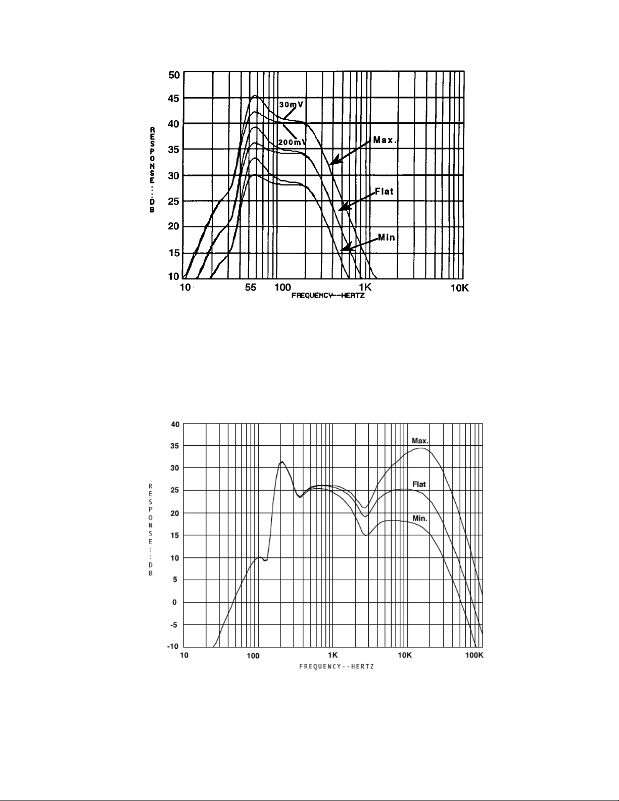
Frequency Response Curves
AM-3P II bass channel frequency response with bass control at min., max. and flat
positions for 30 and 200 mVrms input level. A boost occurs at 55Hz for low input
levels-i.e.-30mV. The gain measurements in this graph should be referenced to the
input level.
Figure 1. Bass Channel Frequency Response Curve
AM-3P II left/right channel frequency response with treble control at min., max. and
flat positions. The gain measurements in this graph should be referenced to the
input level.
Figure 2. Left/Right Channel Frequency Response Curve
5
Page 6
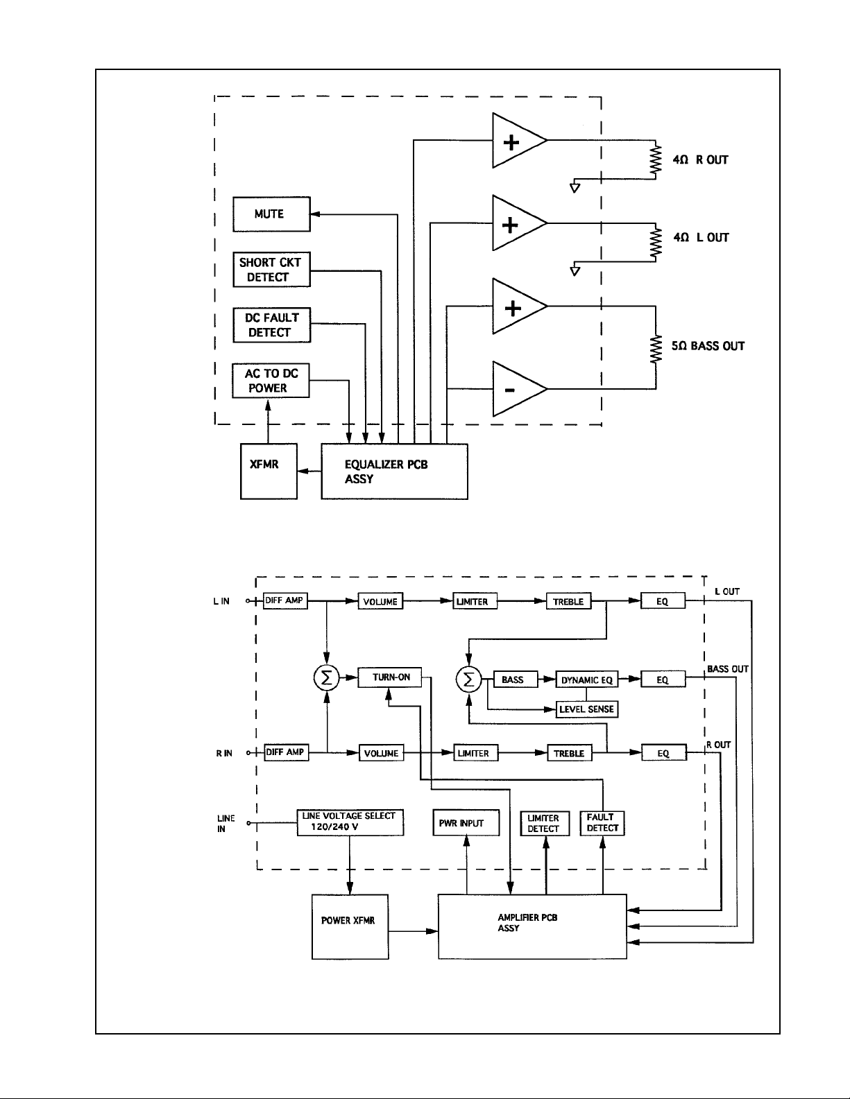
BLOCK DIAGRAMS
Figure 3. AM-3P II Amplifier PCB Assembly Block Diagram
Figure 4. AM-3P II Main PCB Assembly Block Diagram
6
Page 7

AM-3P II THEORY OF OPERATION
NOTE: The following discussion references the AM-3P II/Multimedia Main and Amplifier
PCB schematics, and block diagrams. The block diagrams, Figures 3 and 4, can be found
on page 6 and the schematics are located in the back of this service manual.
GENERAL
The AM-3P II powered Acoustimass
Home Audio and Multimedia. Both variations can be used with the Bose
®
loudspeaker system is manufactured in two variations:
®
Lifestyle® Music
System or other sources that have line-level outputs. The multimedia variation was designed
specifically for computer sound amplification. The basic differences of the multimedia are as
follows:
• 10dB higher gain to accommodate the lower output level of computer sound cards.
• Higher input impedance for compatibility with most industry standard audio equipment.
• RCA input jacks allow mixing of two separate stereo signals (Source 1 and Source 2 inputs).
®
The AM-3P II is based acoustically on the AM-3P Series I Acoustimass
powered loudspeaker system. The distinguishing difference between Series I and Series II is the change
to a new satellite enclosure (AM-4), and equalizer PCB assembly designed to compensate
for the acoustic differences of this new enclosure. Listed below are some of the features of
the AM-3P II.
• Automatic turn-on/turn-off mute of the amplifier output stage
• Automatic (BOSE
®
patented) dynamic equalization
• Bi-amplification for better power distribution to speakers
• Active equalization for smoother frequency response
• Amplifier short-circuit and DC offset fault protection
• Local volume/sensitivity control
• Bass/treble room compensation controls
• Differential input stage (to reject hum)
• Dynamic compressor to prevent amplifier output overload distortion
BLOCK DIAGRAM DESCRIPTION
NOTE: In the discussion of L/R (left/right) channels, only the right channel is discussed. The
left channel operation is identical.
1. Power Supply
A single, universal, 115/230V EI core power transformer is used to power the system. It has
been specially designed for minimum magnetic flux leakage and stand-by power consumption.
The transformer primary remains energized (always on) except when the power switch is in the
off position.
7
Page 8

The two primary windings of the transformer are wired in series for 230V operation, and in
parallel for 115V operation, depending on the position of the customer accessible voltage
select switch. If the system is accidentally energized at 230V with the switch in the 115V
position, the replaceable fuse (F1 located on the Main PCB assembly), will open the circuit
within two minutes. This will be the only damage to the system.
A non-serviceable thermal fuse is located inside the transformer to limit the maximum
temperature to 145 °C under abnormal conditions. However, in most cases the external fuse
(F1) should fail before the internal transformer thermal fuse. The thermal fuse can be checked
by measuring the continuity between pins 1 and 4 (black and white wire) of the primary
connector. This connector is located on the Main PCB.
2. Differential Input Stage
Audio input applied at the phono jack (J8) connects directly to the right (left) differential amplifier
buffer. This stage accomplishes several functions:
• Provides rejection of common-mode interference (such as hum) that might be picked up
by the long audio cable between the AM-3P II and Lifestyle
®
music center
• Provides input overload and ESD protection through diodes (D101-D104)
• Removes radio frequency interference through C103, C125, C127
• Provides DC blockage by C101,102
• Provides a 6 dB gain through op-amp U101.
3. Compressor/Treble Stage
U102 (pins 1, 2, 3) with potentiometer VR2 at the center position, operates as a conventional
inverting operational amplifier stage with a gain of 6 dB. However, when voltage overload is
present at the speaker outputs, transistor array U1 (pins 1, 2, 3) receives a turn-on signal from
the compressor detect stage. Under this condition, the transistor acts as a variable resistor to
ground, and with R107, forms a resistor divider network that attenuates the audio signal. The
amount of attenuation and timing action is carefully controlled by the compressor detect stage
(to be discussed later).
Potentiometer VR2 adjusts the amount of treble boost or cut. In the full counterclockwise
position, the wiper (pin 4) shorts to pin 1. The maximum boost and cut frequency response
graph is shown in Figure 2 on page 5.
8
Page 9

4. High Frequency (HF) Equalization
High frequency equalization and crossover is achieved through three cascaded active EQ
stages. These stages consist of U103, U104 and U105. The purpose of equalization is twofold:
• It provides very sharp low frequency attenuation below 200 Hz (the crossover frequency)
to prevent overload of the L/R speakers
• It provides finely tailored correction in the speaker passband so that overall frequency
response of the system is acoustically correct
The U103 stage is a combination 2
nd
order 200 Hz high-pass filter and 5 dB 2 kHz dip notch filter.
The U104 stage provides the 5 dB peak at 200 Hz and the sharp band-reject between 100 and
200 Hz. Finally, the U105 stage is a combination 2
nd
order 20 kHz low-pass filter and 2 dB 350
Hz notch filter.
5. Bass Control
The bass channel signal is derived from the sum of the left and right channels through resistors
R129 and R229 and through inverting op-amp summer U2. Potentiometer VR3 simply adjusts
the gain of the stage between -6 dB to +6 dB. In the flat (center) position of the control ,the gain
is 0 dB. Adjusting the bass by varying the gain of the overall bass channel has been determined
to be acoustically appropriate to compensate for various placement options of the bass module.
6. Automatic Dynamic Loudness
In order to compensate for the ear’s loss of bass response at low listening levels, a BOSE
patented (4,739,513) automatic loudness circuit is employed. This circuit automatically senses
the volume level of the incoming audio signal and properly adjusts the amount of low frequency
bass boost. When the volume level is high, the frequency response of the circuit is flat. When
the volume level is decreased (at the music center), the low frequency gain is increased in the
region between 50 and 150 Hz (see the bass channel frequency response graph, Figure 1 on
page 5). This loudness contour, and the time constants associated with it, have been precisely
determined through psycho-acoustic testing and should not be confused with other conventional loudness schemes.
®
Circuit operation is as follows: Left and right audio output at pins 7 and 1 of U101 are summed
together by resistors R132 and R232. The AC signal at pin 3 of level detect op-amp U2 is
negative-peak detected and is presented across emitter resistor R9. The peak detected signal
has a (approximate) 4 second hold time and a 4 sec/10 dB release time constant which is
developed within the feedback loop of U2 (pins 1, 2, 3). The voltage across R9 is converted to
a current source through transistor Q3, and flows into pin 5 of transconductance amplifier U4.
U4 is placed in the feedback loop of op-amp U3 to create an inverse voltage controlled
bandpass stage such that increased current into pin 5 of U4 causes the gain of the bandpass
stage to decrease. The 55 Hz bandpass filter consists of resistors R10, R11 and R15 and
capacitors C6 and C7. At frequencies above 200 Hz, the stage acts as a unity gain follower (flat
frequency response) through resistors R16, R17 and R18. The overall loudness contour
response is visible at U3 pin 1.
9
Page 10

7. Low Frequency (LF) Equalization
Low frequency bass channel equalization and crossover is accomplished in two active filter
stages. The first stage consists of op-amp U3 (pin 5, 6, 7), capacitors C9 and C10 and resistors
R19, R20, and R21. It creates the sharp band-reject attenuation below 50 Hz. The second
stage consists of op-amp U5 (pin 1, 2, 3) capacitors C13 and C14, and resistors R24, R25, R26
and R27. It acts as a combination 2
nd
order 50 Hz high-pass and 200 Hz low-pass filter. The
combined response of these two stages is shown in the bass channel frequency response
graph in Figure 1 on page 5.
8. Auto Turn-On/Off Mute
An improved version of auto turn-on/off is used in the AM-3P II. A separate 3.5 mm stereo mini-
®
jack (J7) is used to receive the turn-on signal from the serial data output of the Lifestyle
music
center. When the 3.5 mm plug is inserted, the audio sense circuit is disabled and the amplifier
outputs will only unmute if the DC control signal is present at J7 pin 3. This action occurs
through the built-in DPDT switch in J7 which connects J7 pin 3 directly to the Q9 mute circuit.
Therefore, the system is not subject to random false turn-on (from electrical noise, etc.) when
used with the Lifestyle
When the AM-3P II is used with a source other than the Lifestyle
®
music center.
®
music center, the stereo miniplug is not inserted into the jack, and therefore mute transistor Q9 is directed to the output of
the audio detect comparator U6 (pin 5, 6, 7). This comparator uses hysteresis to achieve a
positive turn-on of at least 90 seconds before the system will revert to stand-by (mute) mode
after removal of the audio signal.
9. Compressor Detect
The output of each left/right amplifier is half-wave detected through diodes D108 and 208. This
voltage is divided down by R53 and R54 and presented at the emitter of Q12. Power supply
voltage is similarly divided down by R50 and R51 and presented at the base of Q12. Diodes
D13 and D14 simulate the saturation voltage drop that occurs in the power amp stage.
Therefore, when the audio output of any amplifier comes within 2 volts of the instantaneous
power supply voltage, Q12 will conduct. This signals the compressor (limiter) to act. Current
from Q12 charges hold capacitor C35 and releases capacitor C36. Voltage at C35 is buffered
by transistor U1 (pins 5, 6, 7) and decreased down to a logarithmic voltage by resistor R67 and
diode U1 (pins 12,13,14). This voltage is then presented to the base of compressor transistors
U1 (pins 1, 2, 3) and U1 (pins 8, 9, 10) which are described in the compressor section.
The DC control voltage present across capacitor C35 is derived through the use of an improved
hold and release characteristic, resulting in lower compressor distortion. In conventional
limiters, this DC control voltage is derived by a simple series diode and parallel RC network to
ground. Unfortunately, for low frequency overload, this results in substantial ripple voltage
present on the DC gain control voltage. This results in the all too common problem of mid-range
voices or instruments being badly “modulated” by low frequency overload. This problem is
solved by having two separate capacitors, one that “holds” the smooth DC voltage just long
enough to prevent low frequency ripple (approximately 40ms) and the other (C36) which quickly
releases the hold capacitor (through diode D17) at the proper time to maintain overall 100ms
release time.
10
Page 11

10. Power Amp (Amplifier PCB)
Four identical topology class B, power amplifier stages are used to create the three power
amplifier channels. One each is used for the left and right power amplifiers (2 x 20W into 4 Ohm),
and two are used in bridged mode for the bass channel to create 50W into 5 Ohm. Operation
of the left channel (representative) is as follows:
A positive signal at op-amp input U106 pin 3 causes op-amp supply current to flow into pin 7
(and out through pin 6) through Q103. Q103 is used simply to buffer the +20V high voltage
supply down to a safe +7.4V for the op-amp. This current also flows through R132 and diode
D105. R132 and D105, together with driver transistor Q105 and R134 form a current mirror
which multiplies the current through Q103 by the ratio R132/R134. This increased current flows
through driver transistor Q105, and into the base of output transistor Q107. The hFE current
gain of output transistor Q107 (about 100) provides final current amplification before reaching
the speaker output.
The power amplifier topology is complementary. Therefore, operation of the amplifier on
negative half cycles is identical to positive cycle operation, except for component reference
designations.
11. Short-Circuit Protection
Left and right power amp stages have short circuit protection. This is necessary to prevent
damage to the amplifier from customer misuse that might occur, for instance, if the customer
were to accidentally short the speaker cable wires that connect to the cube speakers. If this
happens, all three amplifiers will momentarily mute for about 3-4 seconds and continue to mute
until the abnormal condition is removed.
Short circuit protection is achieved with the use of a .1
Ω resistor (R146 for left channel) in series
with each amplifier output. Under normal conditions, peak current to the 8 Ω speakers should
never exceed 3.5A. If current flow momentarily exceeds 5.0A, then Q109 will conduct and
trigger monostable multivibrator circuit U5 (pins 5, 6, 7) on the Main PCB. Pin 7 will go high
(for about 3 seconds) and through diode D12 will trigger mute transistor Q10. Turn-on of Q10
causes all three amplifiers to mute. Referring to the left channel power amplifier, actual muting
occurs by turning on transistors Q110, Q101, and Q102 which cause both driver transistors
Q105 and Q106 to turn off. When the driver transistors are off, there can be no current flow
through the output transistors, which results in no current flow to the speaker.
11
Page 12

12. DC Offset Protection
If any one of the three amplifier channels should fail, it is likely that a large DC voltage will occur
at the output of that channel. If this occurs, the DC offset detect circuit will cause the AM-3P II
amplifier power supply to shut down. It will remain shut-down until the unit is unplugged from
the power source. This provides a safe indication to the customer that the unit requires service.
Detailed operation is as follows: The amplifier outputs are summed by resistors R149, R249,
R318, and R418, and (low pass) filtered by capacitor C29. For a sustained DC offset, C29 will
charge either negative or positive. A positive offset will trigger Q7 and a negative offset will
trigger Q8. This in turn causes Q6 to conduct and latches Q5 permanently on. Q5 then shorts
the emitter of Q4 to ground (off). Q4 is the transistor that controls turn-on of 2P1T relay K1 (on
the Amplifier PCB) that is used to connect +/- 20V supply rails to the power amplifiers. Thus,
the amplifiers are de-energized.
12
Page 13

AM-3P II DISASSEMBLY/ASSEMBLY PROCEDURES
Bass Module
NOTE: Refer to Figures 6 and 7 (pages 29 and 30)
for an exploded view of the module. Numbers in
parentheses reference the individual parts displayed
in these Figures.
1. Cover Removal
A. Remove the cover cap (1) by using the flat
edge of a screwdriver or your fingers. Find the
recess on one side of the cap and lift the cap up
and away from the cover (3).
B. Remove the screw (2) located under the cover
cap.
C. Pull the 3 (friction fit) control knobs (4) directly
out from the module.
D. Stick your fingers into the control knob holes.
Swivel the cover carefully away from the Main
PCB connector panel (5) and pull it away from
the module.
2. Cover Replacement
3. Main PCB Assembly Removal
A. Remove 3 screws (6) that secure the Main
PCB (5) to the adapter bracket (8).
IMPORTANT: The connector gasket (7) has a
light adhesive backing. Be careful not to tear it
during removal.
B. Pull the connector gasket carefully away from
the PCB connector panel.
C. Release the PCB from the 4 adapter bracket
snaps (not shown), one edge at a time.
D. Unplug the flat, 16-pin cable (13) connecting
the Main PCB to the Amplifier PCB (11).
E. Disconnect the 5-pin connector housing, J5,
(which is connected to the transformer
assembly’s (18) primary side), by pulling the PCB
carefully up from the unit. Unhook the connector
housing from the slot on the adapter bracket (see
balloon view in Figure 6).
A. Hook the cover (3) into place by slanting the
cover slightly forward (with connector panel
facing you) and aligning the appropriate holes
with the PCB connector panel.
B. Snap the cover into place.
C. Replace the 3 control knobs (4) by pushing
them in towards the module. The knobs are
keyed and will only fit one way.
D. Secure the cover to the module with 1 screw
(2).
E. Hook the cover cap (1) into place. The
notched edge must align with the module’s label
side.
IMPORTANT: The J5 connector pins fit snugly
into the mating connector housing. Take care
when attempting to unhook this connector.
4. Main PCB Assembly Replacement
A. Hook the J5 connector housing into the slot on
the adapter bracket (8). See the balloon view in
Figure 6.
NOTE: Connector J5 has a unique keying feature
and can only be connected one way.
B. Lower the PCB (5), solder side up, into
position. The PCB’s connector panel must align
with the module’s label side. Make sure that the
pins on connector J5 line up with it's mating
connector housing (transformer primary wires).
13
Page 14

C. Push down the corners of the PCB until all 4
adapter bracket snaps (not shown) engage.
Make sure that the J5 connector pins are
completely inserted into the mating connector
housing.
D. Plug in the flat, 16-pin cable (13) to the PCB.
7. Amplifier PCB Assembly Removal
NOTE: It is not necessary to completely
disassemble the unit to access the Amplifier PCB
(11). Follow the simplified steps A-D below if
direct access to this PCB is required and you
have not already disassembled the unit.
E. Secure the PCB to the adapter bracket with 3
screws (6).
F. Place the connector gasket (7) over the
connector panel.
5. Adapter Bracket and Heatsink Removal
NOTE: It is only necessary to remove 3 screws
(10) to remove the adapter bracket (8). These
screws are located on the same side as the
module’s labels. The bracket hooks onto a flange
that is part of the heatsink (9). If further
disassembly of the unit is required, then all 6
screws (10) should be removed.
A. Remove 6 screws (10) that secure the adapter
bracket and the heatsink to the module.
B. Pull the bracket and heatsink away from the
module.
A. Remove the cover (3) using Procedure 1.
B. Unplug the flat 16-pin cable (13) connecting
the Main PCB to the Amplifier PCB.
C. Remove 6 screws (10) that secure the adapter
bracket (8) and heatsink (9) to the module.
D. Lift the Main PCB (5), adapter bracket and
heatsink away from the module.
NOTE: The Main PCB should remain connected
to the transformer primary side. It should also
remain secured to the adapter bracket with 3
screws (6).
E. Lift up the Amplifier PCB (11) and unhook
connectors J1 and J4 from the PCB. J4 is
connected to the woofer and J1 is connected
to the transformer assembly’s (18) secondary
side. Pull the PCB away from the unit.
NOTE: The Amplifier PCB Assembly (11) may be
stuck to the heatsink with thermal grease.
6. Adapter Bracket and Heatsink Replacement
A. Lower the heatsink (9) into position on top of
the Amplifier PCB (11). Make sure that the side
of the heatsink with smaller fins is aligned with
the module’s label side.
B. Align the screw holes on the heatsink with
those on the transformer cup (19).
C. Hook the adapter bracket (8) onto the heatsink
flange. Lower the adapter bracket into position.
The bracket has screw holes only on one side.
These should be aligned with the screw holes on
the module’s label side.
D. Secure the heatsink and adapter bracket to
the module with 6 screws (10).
F. Remove the two transistor spring clips (14)
that rest on the transformer cup (19).
8. Amplifier PCB Assembly Replacement
A. Place the two transistor spring clips (14) on
the transformer cup (19).
B. Connect the J4 connector to the safetycontrolled woofer cable (24) and connector J1 (5
pin) to the transformer assembly’s (18)
secondary side. When facing the module's label
side, the transformer's secondary side is on the
right.
NOTE: The large capacitors on the Amplifier
PCB (11) fit into one side of the transformer cup
(19).
14
Page 15

C. Lower the PCB (solder side up) into place on
top of the transformer cup. There are holes in
each corner of the PCB that align with the locator
pins on the cup. The transistors (on PCB edges)
should rest lightly on the transistor spring clips
(14). Place the transformer primary connector
wires into the slot on the PCB.
B. Align the screw holes on the transformer with
those on the cup.
C. Secure the transformer to the cup with 4
screws (15) and 4 washers (16) using a 3/32-inch
Allen wrench.
NOTE: If no further servicing is required, use the
simplified steps below to reassemble the unit.
D. Replace the heatsink (9) using Procedure 6,
steps A and B.
E. Place the transformer primary into the slot on
the Amplifier PCB (11).
F. Secure the adapter bracket (8) and Main PCB
(5) using Procedure 6, step C.
G. Secure the heatsink, adapter bracket and
Main PCB to the module with 6 screws (10).
H. Replace the cover (3) using Procedure 2.
9. Transformer Assembly Removal
NOTE: If direct access to the transformer is
required and the unit has not been
disassembled, refer to the simplified steps
provided in Procedure 7, along with step A of
this procedure.
A. Remove 4 screws (15) and 4 washers (16)
using a 3/32-inch Allen wrench and lift the
transformer assembly (18) out of the transformer
cup.
NOTE: If no further servicing of the unit is
required, refer to the simplified steps provided in
Procedure 8 to reassemble the unit.
11. Transformer Cup and Gasket Removal
NOTE: To directly access the transformer cup
and gasket, follow the simplified steps provided
in Procedure 9, then proceed with steps A and
B of this procedure.
A. Remove 2 screws (10) that secure the
transformer cup (19) to the module and lift the
transformer cup away from the module.
NOTE: There might be woofer connector wires
(safety controlled cable (24)) taped over the
transformer cup gasket (20). Note the location of
the cable relative to the module. Remove the
tape and move the wires aside.
B. Remove the transformer cup gasket.
12. Transformer Cup and Gasket Replacement
NOTE: The transformer cup gasket (20) has
raised edges that should be face up when
positioned in the transformer cup. The gasket
also has a U-shaped opening that aligns
precisely with the module.
NOTE: With the module’s label side facing you,
the transformer’s primary side is on the left and
the secondary side is on the right.
10. Transformer Assembly Replacement
NOTE: The transformer bracket (part of the
assembly) has a bent flange in one corner that
will only allow the transformer to fit in the
transformer cup (19) one way.
A. Lower the transformer assembly (18) into the
transformer cup.
A. Place the gasket in position over the opening
of the module.
B. Lay the woofer cable (24) over the appropriate
corner of the bass module. The wires must cross
over the top of the gasket.
C. Position the transformer cup. The cup has a
locating ridge and only fits into the module one
way. The lip should be aligned with the U-shaped
opening in the module.
15
Page 16

D. Secure the cup to the module with 2 screws
(10).
NOTE: If no further servicing of the unit is
required, refer to the simplified steps provided in
Procedure 10 to reassemble the unit.
13. Woofer Removal
C. Remount the woofer (21) to the module using
4 screws (22). Repeat the woofer test
procedures.
NOTE: If no further servicing of the unit is
required, use the following simplified procedures
to reassemble the unit.
NOTE: If direct access to the woofer is required
and the unit has not already been disassembled,
use the following simplified steps A-D.
A. Remove the cover (3) using Procedure 1.
B. Remove the Main PCB (5), heatsink (9) and
adapter bracket (8) using Procedure 7, steps C
and D.
C. Lift up the Amplifier PCB (11) and unhook the
safety controlled woofer cable (24) from the J4
connector (Amplifier PCB).
D. Remove the transformer cup (19) and gasket
(20) using Procedure 11.
E. Remove 4 screws (22) that secure the woofer
(21) to the baffle (part of the module). See
Figure 7.
14. Woofer Replacement
NOTE: Refer to Figure 7 for an exploded view.
D. Replace the transformer cup (19) and gasket
(20) using Procedure 12.
E. Replace the transformer assembly (18) using
Procedure 10.
F. Reinstall the Amplifier PCB (11) using
Procedure 8.
G. Reinstall the heatsink (9) and adapter bracket
(8) using Procedure 6.
H. Reinstall the Main PCB (5) using Procedure
4.
I. Replace the cover (3) using Procedure 2.
Satellite Procedures
NOTE: Refer to Figure 8, page 30 for an
exploded view of the satellite. Numbers in
parentheses reference the individual parts
displayed in this figure.
A. Carefully lift the woofer out and cut the wires
connected to the woofer terminals as close to the
terminals as possible.
NOTE: Make a note of the woofer terminal
orientation relative to the module. The woofer
should be repositioned in it's original location.
B. Strip the wires and connect to a replacement
woofer. Make sure that the red wire is connected
to the positive (+) terminal and the black wire is
connected to the negative (-) terminal. When
repositioning the woofer, make sure that the
woofer gasket (23) is correctly positioned behind
the woofer to make an airtight seal.
1. Grille Removal
Hold the satellite enclosure (5) with one hand.
Use your other hand to squeeze and pull the
grille assembly (1) away from the satellite
enclosure.
2. Grille Replacement
Align the grille assembly so that the curved
edges are at the top and bottom of the enclosure.
The nameplate (7) should be at the bottom right
corner of the enclosure. Snap the grille gently
into place.
16
Page 17

3. Twiddler Removal
7. Connector Removal
A. Remove Grille from enclosure. Use
Procedure 1.
B. Remove the 4 screws (3) holding the twiddler
(2) in place. Lift the twiddler out and cut the wires
connected to the twiddler as close to it's
terminals as possible.
4. Twiddler Replacement
A. Strip the wires and connect them to the
replacement twiddler (2).
NOTE: The positive (+) terminal of each twiddler
is marked with a red dot.
B. Connect the red wire to the positive (+)
twiddler terminal and the black wire to the
negative (-) twiddler terminal.
C. Lower the twiddler into the satellite enclosure
and secure the twiddler to the enclosure with 4
screws (3). Repeat the satellite test procedures.
Use Procedure 1 and 3 to access the inside of
the satellite enclosure.
A. After the twiddler has been removed, pull out
the polyester batting (4) from the enclosure.
B. Use a pair of pliers to press the connector's
(6) release snaps together. Push the connector
out of the enclosure.
C. Cut the wires to the connector as close as
possible.
8. Connector Replacement
A. Strip the wires and connect them to the
replacement connector (6).
NOTE: The positive (+) terminal is marked red.
B. Connect the red wire to the positive (+)
terminal and the black wire to the negative (-)
terminal.
D. Return the Grille Assembly to the front of the
Satellite Enclosure.
C. Press the terminal into the back of the
enclosure until it snaps into place.
17
Page 18

AM-3P II TEST PROCEDURES
Satellite Test Procedures
NOTE: These procedures test the satellite
without the bass module.
1. Sweep Test
A. Connect an oscillator to a power amplifier.
Adjust the amplifier output to 4 Vrms. Connect
the amplifier leads to the satellite (cube speaker)
input terminals. Sweep the oscillator from 100 Hz
to 5 kHz. If any twiddler buzzes or sounds
distorted, replace it.
2. Phase Test
IMPORTANT: Supply voltage should only be
momentarily applied to the satellite input
terminals to avoid possible damage to the
twiddlers.
A. Set a DC power supply to 8 volts. To ensure
that each twiddler is connected in phase, connect
the positive supply lead to the positive (+)
satellite input terminal (red) and the negative
supply lead to the negative (-) satellite input
terminal (black). The twiddler should move
outwards with the application of the supply
voltage.
NOTE: If any twiddler cone deflects inwards or
does not move, check all connections.
Woofer (Module) Test Procedures
NOTES: These procedures test the bass module
without the satellites. All tests should be
performed with the bass and treble control knobs
in the normal or "detent" position and the volume
control knob at maximum volume.
It may be necessary to disassemble the module
in some of these procedures. Refer to the
Disassembly/Assembly Procedures section for
specific instructions.
1. Turn-On Test
NOTES: Refer to the AM-3P II Main PCB
schematic for the location of the J7 mini-jack
input, pins 1 and 3. The On/Off Control Circuit
is located on this schematic.
This test can be performed with a fully
assembled module.
This procedure also refers to the “ring” and
“sleeve” of a standard 3.5 mm mini-jack.
A. Connect an oscillator to the module’s L/R
audio input terminals. Adjust the oscillator to 500
Hz, 220 mVrms.
B. Insert a 3.5 mm mini-jack into the input
terminal labeled “System Control”. The audio
signal should mute.
C. Set a DC power supply to 8 volts and apply
this voltage between pins 3 (ring) and 1 (sleeve,
which is connected to ground) of the mini-jack.
The audio signal should return.
2. Sweep Test
NOTE: This test can be performed with a fully
assembled module.
A. Connect an oscillator to the module’s L/R
audio input terminals. Adjust the oscillator to 100
Hz, 220 mVrms. Sweep the oscillator from 10300 Hz. There should not be any loud,
extraneous sounds. If there are any loud buzzes
or distortion, replace the woofer.
NOTE: There should not be any buzzes or rattles
from within the module. Redress any wire or
component that buzzes or rattles.
18
Page 19

3. Tone Control Test
Frequency Relative Response
NOTE: This test can be performed with a fully
assembled module.
A. Connect an oscillator to the module’s L/R
audio input terminals. Adjust the oscillator to 100
Hz, 220 mVrms.
B. Rotate the bass control knob fully clockwise
and counterclockwise from it's center or “normal”
position. The bass level should increase and
decrease cleanly without making a scratchy
noise. Clean or replace any potentiometer that
makes this noise.
C. Repeat this procedure for the treble control
using a frequency of 4 kHz.
4. Frequency Response of L/R (Twiddler)
Channels
NOTE: This test can be performed with a fully
assembled module.
A. Connect an oscillator to the module’s L/R
audio input terminals. Adjust the oscillator to 1
kHz, 200 mVrms. Connect a piece of test
equipment capable of measuring decibels to
either the left or right twiddler output terminals
(labeled “To Cube Speakers”). Measure the dBs
at this setting and use this as a 0 dB reference.
B. Once the left or right output terminals of the
cube speaker are connected, adjust the oscillator
frequency and measure the relative response
according to the chart located at the end of this
procedure.
360 Hz -2.1 dB ± 1.5 dB
1 kHz 0 dB
2 kHz -3.5 dB ± 1.5 dB
10 kHz -.4 dB ± 1.5 dB
20 kHz -2.9 dB ± 2.0 dB
5. Twiddler Power Output Test
NOTE: This test can be performed with a fully
assembled module.
A. Connect a 4Ω resistive load across the left or
right twiddler output terminal (labeled “To Cube
Speakers”). Connect a voltmeter across the
load.
NOTE: These measurements can be obtained at
120 and 240 V. Results will vary depending on
the line voltage used.
B. Connect an oscillator to the module’s L/R
audio input terminals. Adjust the oscillator to 1
kHz, 454 mVrms.
C. Measure the voltage across the load. It should
be approximately 8.9 volts (20 watts). The
signal should look undistorted when viewed on
an oscilloscope.
6. Twiddler Short Circuit Protection Test
C. Repeat this test for the other channel.
Frequency Relative Response
100 Hz -15.6 dB ± 2.0 dB
200 Hz +5.7 dB ± 1.5 dB
NOTES: This test can be performed with a fully
assembled module.
IMPORTANT: Do not short out for longer than 1
second.
A. Adjust the oscillator to 1 kHz, 200 mVrms.
Short the left or right twiddler output terminal.
The signal should mute for approximately 3
seconds.
19
Page 20

7. Air Leak Test
9. Woofer Phase Test
NOTE: Part A of this test can be performed with
a fully assembled module.
A. Connect an oscillator to the module’s left/right
(L/R) audio input terminals. Adjust the oscillator
to 40 Hz, 1 Vrms. Listen for air leaks around the
transformer cup gasket. If there is a “whooshing”
noise, there is probably an air leak around the
gasket. Refer to the Disassembly/Assembly
Procedures section for instructions on accessing
this gasket. Reposition the transformer cup
gasket under the cup to make an airtight seal.
NOTE: In order to perform the remaining
procedures, it is necessary to disassemble the
module to the woofer level. Leave all connections
intact to perform these tests. Remove the cover
using the procedures in the Disassembly/
Assembly Procedures section. Remove 6
screws that secure the heatsink to the module.
Remove 2 screws that secure the transformer
cup to the module. Slide out the transformer cup
and PCBs carefully. Lay the module on it's side
to access the woofer more easily.
B. Using the same oscillator setting as part A,
listen for air leaks around the woofer gasket. If
there is a "whooshing" noise around the gasket,
reposition the woofer gasket behind the woofer to
make an airtight seal.
A. Disconnect the woofer (connector J4) from the
Amplifier PCB. Set a DC power supply to 8
volts. Connect the positive supply lead to the
positive (+) woofer connection (red) and the
negative supply lead to the negative (-) woofer
connection (black). The woofer should move
outwards with the application of the supply
voltage.
10. Frequency Response of Bass Channel
NOTES: Pull the heatsink away from the
Amplifier PCB to expose the board's solder
side. It will be necessary to access the woofer
output connector (J4) to perform the remaining
procedures.
Bass amplifier output measurements are made
across J4 pins 1 and 2. The amplifier uses a
bridged output. Do not connect either output to
ground. Any test equipment that will be
connected to these points must be floated, or
isolated from ground.
A. Make up a temporary set of connections to the
woofer output connector J4.
B. Connect an oscillator to the module’s L/R
audio input terminals. Adjust the oscillator to 100
Hz, 200 mVrms.
8. Woofer Rub and Tick Test
A. Connect an oscillator to the module’s L/R
audio input terminals. Adjust the oscillator to 10
Hz, 1.5 Vrms. No extraneous noises such as
rubbing, scraping or ticking should be heard.
NOTE: To distinguish between normal
suspension noise, rubs or ticks, displace the
cone on the woofer slightly with your fingers. If
the noise can be made to go away or get worse,
it is a rub or a tick and the woofer should be
replaced. If the noise stays the same, it is normal
suspension noise and the woofer is fine.
Suspension noises will not be heard with
program material.
C. Connect a piece of test equipment capable of
measuring decibels to the woofer output
connector J4. Make sure that the meter is not
grounded. Measure the decibels at this setting
and use as a reference for all other readings.
D. Adjust the oscillator frequency and measure
the relative response according to the chart
located at the end of this procedure (next page).
20
Page 21

Frequency Relative Response
20 Hz -18.0 dB ± 2.0 dB
C. Measure the voltage across the load. It should
be approximately 15.8 volts (50 watts). The signal
should look undistorted when viewed on an
oscilloscope.
55 Hz +1.8 dB ± 1.5 dB
100 Hz 0 dB
200 Hz -0.5 dB ± 1.5 dB
400 Hz -10.7 dB ± 1.5 dB
11. Bass Channel Dynamic EQ Gain
NOTE: Use the same test setup as Procedure 10.
A. Adjust the oscillator to 100 Hz, 30 mVrms. Use
this as a reference point.
B. Adjust the oscillator to 55 Hz. There should be
a boost of approximately 5 dB. (A 3.0 dB ± 1.0 dB
difference between the 30 mV and the 200 mV
input level). Refer to the chart in the previous
procedure.
Complete System Tests
NOTE: Use these procedures when a complete
AM-3P II system (module and satellites) is to be
serviced.
1. System Phase Test
Use the procedures already listed for the satellites
and the module. Use Procedure 2 under Satellite
Test Procedures and Procedure 9 under Module
Test Procedures.
2. System Sweep Test
Use the procedures already given for the satellites
and the module,except use 220 mVrms for both
parts of the test. Use Procedure 1 under Satellite
Test Procedures and Procedure 2 under Module
Test Procedures. Make sure that the satellites are
connected to the bass module.
3. All Other Tests
12. Woofer Power Output Test
NOTE: Use the same test setup as Procedure 10,
except remove the dB meter. Make sure that any
test equipment connected to the woofer output is
floated or isolated from ground.
A. Connect a 5Ω resistive load to the woofer
output. Connect a voltmeter across the load.
NOTE: These measurements can be obtained at
120 and 240 V. Results will vary depending on the
line voltage used.
B. Connect an oscillator to the module’s L/R audio
input terminals. Adjust the oscillator to 100 Hz,
345 mVrms.
All other tests listed under Module Test
Procedures can be used to test a complete
system.
21
Page 22

Figure 5. 120/240V Transformer Schematic
Secondary Load Line (@ Nominal Primary Voltage):
Vout = 21.0 Vdc Maximum (Referenced to C.T.) @ No Load
Vout = 14.0 Vdc ± 5% (Referenced to C.T.) @ Idc = 3.2 A
V1 = 10.0 Vrms ± 10% (Referenced to C.T.) @ No Load
Exiting Current @ 10% High Line: 200mA @ 132 Vrms, 60 Hz
300mA @ 264 Vrms, 50 Hz
Primary Voltage: 120 Vrms, 60 Hz Nominal (Test Circuit A)
240 Vrms, 50 Hz Nominal (Test Circuit B)
22
Page 23

INTEGRATED CIRCUIT DIAGRAMS
14
13
12
12
3
11
NPN
4
10
56
8
9
7
Quad Transistor Array, NPN
P/N 145317 (MPQ3904)
Main PCB Assembly
U1
Pin
1 Collector
2 Base
3 Emitter
4 No Connection
5 Emitter
6 Base
7 Collector
8 Collector
9 Base
10 Emitter
11 No Connection
12 Emitter
13 Base
14 Collector
A Output
A -Input
A +Input
V
1
2
3
_
4
Dual Operational Amplifier, DIP-8
P/N 108568 (RC 4559)
Main PCB Assembly
U2, U3, U5, U6, U101-105
+
8
7
6
5
V
B Output
B -Input
B+Input
23
Page 24

NC
IN-
IN+
1
8
NC
Pin Pin
Comment
Name
2
7
+
V
1 NC No Connection
2 IN- Inverting Input
3 IN+ Non-inverting Input
3
+
6
Output
4 V- Negative Power Supply Input
5I
ABC
Amplifier Bias Input
6 Out Amplifier Output
7 V+ Positive Power Supply Input
4
-
V
= (V+)-(V-)
V
CC
5
INB
8 NC No Connection
Bipolar Operational Transconductance Amplifier
P/N 119834 (CA3080)
Main PCB Assembly
U4
12
3
Pin 146234
NJM78LO8A-T3
146235
NJM79LO8A-T3
1 Output Ground
2 Ground Input
3 Input Output
Amplifier PCB Assembly
+8 Volt Regulator 146234, U1
-8 Volt Regualtor 146235, U2
24
Page 25

Balance
1
8
NC
Input
Input
V
-
2
3
4
Pin Pin
+
Comment
7
6
5
Name
1 N1 Offset Voltage Null Input 1
2 -IN Inverting Input
3 +IN Non-inverting Input
4 V- Negative Power Supply Input
5 N2 Offset Voltage Null Input 2
6 Out Amplifier Output
7 V+ Positive Power Supply Input
8 NC No Connection
+
V
Output
Balance
Single JFET Input Operational Amplifier
P/N 250475-001 (LF355CN)
Amplifier PCB Assembly
U106, U206, U301, U401
25
Page 26

PART LISTS AND EXPLODED VIEWS
The following section contains part lists and exploded views for the AM-3P II powered
speaker system. The part lists and views are broken down as follows:
• Bass Module part list and exploded view. A view of the woofer is
contained in a separate figure.
• Satellite part list and exploded view.
• Packaging part list and exploded view.
• PCB Assembly part lists. PCB layouts and schematics are located in the back of
the service manual.
IMPORTANT: Part changes were recorded by PC board revision level. Before
replacing or ordering parts check the revision number on the PC Board. Compare
the PCB information with the part list, this will provide an accurate way of
determining the value and part number of the replacement part. PC boards are
marked as follows:
1
26
Page 27

AM-3P II Bass Module Part List (Figures 6 and 7)
Item
Number
1 Cap,Cover,White 145105-1 1
Cap,Cover,Black 145105-2 1
2 Screw,Machine,8-32x.5,Pan,XREC 121316-08 1
3 Cover,Black 144590-0222 1
Cover,White 144590-0231 1
4 Knob,Control,White 148839-1 3
Knob,Control,Black 148839-2 3
5 PCB Assy.,EQ,US/International 193567-1 1 1,2
PCB Assy.,EQ,Europe 175302-3 1 1,2
PCB Assy.,Multimedia,
US/International
PCB Assy.,Multimedia,Europe 175302-5 1 1,2
6 Screw,Hilo,6x.5,Pan,XREC 127015-08 3
7 Gasket,Cover-Connector 146208 1
8 Bracket,Adapter,Black 144587-2 1
Description Part Number Qty
Per
Assy
175302-4 1 1,2
*See
Note
9 Heatsink,7.41x5.34x2.11 144588 1
10 Screw,Tapp,8-11x1, pan, XREC/SQ 172672-16 8
11 PCB Assy.,Amplifier 149374 1 1,2
12 Tape Foam,3" 129284-030 1
13 Cable,Flat,16-pin,Terminated 144437 1
14 Clip,Spring,Transistor 144591 4
15 Screw,Shoulder,8-32x.312,Sock,Hex 143444-04 4
16 Washer,Flat,.195" 146981 4
17 Grommet,Isolator,.563" 143445 4
18 Transformer,Power,120/240V 143051 13
19 Cup,Transformer,Black 144589-2 1
20 Gasket,Transformer Cup 143514 1
!
Notes:
1. This part is not normally available from Customer Service. Approval from the Field Service Manager is required before ordering.
2. The individual parts located on the PCBs are listed in the Electrical Part Lists.
3. This part is critical for safety purposes. Failure to use a substitute replacement with the
same safety characteristics as the recommended replacement part might create shock, fire
and/or other hazards.
27
Page 28

AM-3P II Bass Module Part List (Figures 6 and 7)
Item
Number
21 Woofer Assy. 5.25" 143357 1
22 Screw,Tapp,8-11x.75,pan, XRC/SQ 172672-12 4
23 Gasket,Woofer,6.5" 104794-08 1
24 Cable,Speaker 143513 1
Item
Description Part Number Qty
AM-3P II Satellite Part List (Figure 8)
Description Part Number Qty See
Number
1 Grille Assy,Satellite,Black 175177-1 1
Grille Assy,Satellite,Black 175177-2 1
Grille Assy,Satellite,Gray 175177-3 1
Per
Assy
See
Note
Note
2 Twiddler,2.25" 147525 1
3 Screw,Tapp,8-11x.625, Pan,XRC/S 172672-10 4
4 Batting,Polyester,
144225 2
76mmx76mmx50
5 Enclosure,Satellite,Black 175213-1 1
Enclosure,Satellite,White 175213-2 1
Enclosure,Satellite,Gray 175213-3 1
6 Connector,Barrier Gltn,2 Pos,Blk 141405 1
7 Nameplate,Logo,Black 148056-1 1
Nameplate,Logo,Arc. White 148949-2 1
Nameplate,Logo,Gray 148949-3 1
28
Page 29

4
1
2
3
6
3X
5
Main PCB
J5 Connector
Housing
6X
12
4X
10
13
14
17
18
19
PCB Connector
Panel
7
8
9
11
Amplifier PCB
2X
10
15
4X
16
4X
14
24
NOTE: WIRES SHOULD NOT CROSS
UNDER GASKET OR TRANSFORMER
CUP AREA.
Figure 6. AM-3P II Bass Module Exploded View
Transformer
Primary Side
20
Module Label
29
Page 30

24
4X
21
22
23
Figure 7. Woofer Location in Module
6
4
Release Snaps
5
2
3
1
7
Figure 8. Satellite Exploded View
30
Page 31

AM-3P II Packaging List
Item
Number
1 Polybag,14.38x9.87x2 mil 103351 1
2 Manual,Owner's, 174871 1
Manual,Owner's,Multimedia only 175978 1
3 Card,Warranty, Universal 149225 1
4 Envelope,Blank,White 128450 1
5 List,Warranty,Service Stations,
N. America
6 Brochure, All Products,N. America 141478 1
7 Envelope, Warranty Registration,
N. America/International
8 Adaptor,Plug Stereo,Multimedia 128404 1
9 Adaptor,120/230V Polarized,Dual
Voltage
10 Sheet, Instruction Adaptor,Dual
Voltage
11 Sheet,Caution,AM Multimedia 179396 1
Description Part Number Qty
122706 1
123001 1
147013 1
147751 1
Per
Assy
See
Note
12 Cable,Stereo,Phono,Multimedia 176107-1 1
Cable,Stereo Input,5-Pin Connector,
Audio Input
13 Line Cord,Detachable,96",Europe 148203 1*
14 Polybag,13.5x33.5x9.13x3 mil 106595 1
15 Packing,Insert,Corrugated 149253 1
16 Packing,Corner Post,Bass Insert 148364 2
!
Line Cord,120V,Polar
Detachable,US/International
LineCord,230V,Australia,
Detachable
LineCord,230V,UK,
Detachable
143630 1
146999 1 *
134726 1 *
134725 1 *
*This part is critical for safety purposes. Failure to use a substitute replacement with the
same safety characteristics as the recommended replacement part might create shock, fire
and/or other hazards.
31
Page 32

AM-3P II Packaging List
Item
Description Part Number Qty
Number
17 Packing,Cushion 174448 2
18 Wire,18/2 Zip Cord,White,20 ft. 140236 2
Wire,18/2 Zip Cord,Alp White,20 ft.,
136693 2
Multimedia
Wire,18/2 Zip Cord,Black,20 ft. 130915 2
19 Carton,RSC,AM-3P II,US/International 175004-00 1
Carton,RSC,AM-3P II,Ireland 175004-01 1
Carton,RSC,Multimedia 175938-00 1
Carton,RSC,Multimedia 175938-01 1
20 Carton,Alb,Satellite,AM-4 172939 1
21 Bag,Poly,7x9x2 mil,Satellite 175780 1
Per
Assy
See
Note
32
Page 33

17
2X
11
1
3
5
7
9
14
4
10
12
2
6
8
15
2X
16
18
13
Satellites
See Items
20 and 21
19
20
21
Figure 9. AM-3P II Packaging Exploded View
33
Page 34

AM-3P II Main PCB Assembly Part List
Resistors
Reference
Description Part Number Reference
Designator
R1,29,*36,39,41,
43-46,52,59,60,
10.0KΩ,5%,1/8W,
1206
124895-1035
107,132,207,229,
232
*R2 Jumper Chip,1206 124896
R3,5,33,34,38,57,
149,249
R4,17,28,108,130,
208,230
R6,48,56,62 1 MΩ,5%,1/8W,
100KΩ,5%,1/8W,
1206
330Ω,5%,1/8W,
1206
124895-1045
124895-3315
124895-1055
1206
R7,8,*36,42,47,55,
58,68,129
R9,37,49,66,67 2.00KΩ,5%,1/8W,
20.0KΩ,5%,1/8W,
1206
124895-2035
124895-2025
1206
R10 27.4KΩ,1%,1/8W,
124894-2742
1206
R11,15,32,117,217 6.81KΩ,1%,1/8W,
124894-6811
1206
*R112,*212 17.4KΩ,1%,1/8W,
124894-1742
1206
R12,*112,*212 8.25KΩ,1%,1/8W,
124894-8251
1206
R13,24,69 5.11KΩ,1%,1/8W,
124894-5111
1206
R14,*100,*200 10Ω,5%,1/8W,1206 124895-1005
R16,18,35,50,51,
*101,*102,103,104,
1.00KΩ,5%,1/8W,
1206
124895-1025
115,*201,*202,203,
204,215
R19,21 51.1KΩ,1%,1/8W,
124894-5112
1206
R20 2.00KΩ,1%,1/8W,
124894-2001
1206
R22 10KΩ,2%,1/4W,
121243-1211032
52mm,CF
R25 18.2KΩ,1%,1/8W,
124894-1822
1206
R26,27,113,213 24.3KΩ,1%,1/8W,
124894-2432
1206
R30,53 91Ω,5%,1/8W,1206 124895-9105
R31,61,125,225 14.3KΩ,1%,1/8W,
124894-1432
1206
*P/N Change Rev. 1
*See Notes 3 and 4
*P/N at Rev. 0
*See Notes 3 and 4
*See Notes 1 and 2
*P/N Added at
Rev. 1
*See Notes 1 and 2
*See Notes 1 and 2
*See Page 38 for reference column notes.
34
Page 35

AM-3P II Main PCB Assembly Part List
Resistors (Continued)
Reference
Description Part Number Reference
Designator
R40 75.0KΩ,1%,1/8W,
1206
R54 162Ω,1%,1/8W,
1206
*R101,*102,*134,
*201,*202,*234
*R105,*106,*205,
*206
4.99KΩ,1%,1/8W,
1206
3.90KΩ,5%,1/8W,
1206
R109,209 681Ω,1%,1/8W,
1206
R110,210 6.19KΩ,1%,1/8W,
1206
*R111,*211 25.5KΩ,1%,1/8W,
1206
*R111,127,128,
*211,227,228
12.1KΩ,1%,1/8W,
1206
R114,214 34.8KΩ,1%,1/8W,
1206
R116,216 20.0KΩ,1%,1/8W,
1206
*R105,*106,118,
*205,*206,218
17.8KΩ,1%,1/8W,
1206
R119,219 2.37KΩ,1%,1/8W,
1206
R120,123,220,223 1.00KΩ,1%,1/8W,
1206
R121,221 221Ω,1%,1/8W,
1206
R122,124,222,224 100KΩ,1%,1/8W,
1206
R126,226 953Ω,1%,1/8W,
1206
R131,231 1.0Ω,5%,1/4W,
52mm,CF
R133,233 1.0KΩ,,1/4W,2%,
52mm,CF
VR1 Potentiometer,
RTRY,10KΩ,20%,
.05W,Dual
VR2 Potentiometer,
RTRY,10KΩ,20%,
.05W,Dual
VR3 Potentiometer,
RTRY,10KΩ,20%,
.05W,Single
124894-7502
124894-1620
124894-4991
124895-3925
124894-6810
124894-6191
124894-2552
124894-1212
124894-3482
124894-2002
124894-1782
124894-2371
124894-1001
124894-2210
124894-1003
124894-9530
121243-1211R05
121243-1211022
145311
145312
145313
*See Notes 3 and 4
*See Notes 1 and 2
*See Notes 3 and 4
*See Notes 1 and 2
*See Notes 3 and 4
*See Page 38 for reference column notes.
35
Page 36

AM-3P II Main PCB Assembly Part List
Capacitors
Reference
Description Part Number Reference
Designator
C1-4,28,30,32,35,
36,101,102,126,
10uF,20%,16V,105,
EL
201,202,226
C6,7,9,10,13,14,
112,212
C8,120,121,122,
123,124,220,221,
.47uF,5%,50V,85,
BOX
.033uF,20%,50V,
Z5U,1206
222,223,224
C11,103,105,111,
115,203,205,211,
100pF,10%,50V,
1206,SL
215
C12,29,34,104,204 47uF,20%,16V,105,
EL
C15,113,114,213,
214
.12uF,5%,50V,85,
BOX
C16,*106,*206 .0082uF,5%,50V,85,
FILM
C17 33uF,20%,16V,BP,
85,EL
*C106,*206 .0039uF,5%,50V,85,
Film
C107,108,207,208 .082uF,5%,50V,85,
FILM
C109,110,209,210 .0068uF,5%,50V,
85,FILM
C118,218 .001uF,5%,50V,85,
FILM
C119,219 470pF,10%,50V,SL,
DISC
*C125,*127,*225,
*227
*C125,*127,*225,
*227
C31,116,117,216,
217
680pF,10%,50V,SL,
1206
3300pF,10%,50V,
Y5P,1206
.1uF,5%,50V,85,
FILM
137126-100
137127-474
124958-3331
124956-1012
137126-470
137127-124
137123-822
147522-330
137123-392
137123-823
137123-682
137123-102
137269-471
124956-6812
124957-332
137123-104
*See Notes 1 and 2
*See Notes 3 and 4
*See Notes 3 and 4
*See Note 1 and 2
Diodes
Reference
Designator
D2-10,12-15,17,18,
*19, 101-104,108,
201-204,208
*D19 Zener,5.1V 136758-5231
Description Part Number Reference
Switching,75V,
300mA
121501
*See Page 38 for reference column notes.
36
*P/N at Rev. 0
*P/N Change Rev. 1
Page 37

AM-3P II Main PCB Assembly Part List
Reference
Description Part Number Reference
Designator
Q1,5,7-9,11 BPLR,N,60V,
200mA,TO-92
Q2-4,6,10,12 BPLR,P,60V,
200mA,TO-92
Integrated Circuits
Transistors
117921
119168
Reference
Description Part Number Reference
Designator
U1 Transistor,Array,
Quad,N,DIP-14
U2,3,5,6,101-105 Op-Amp,Dual,
DIP-8,RC4559
U4 Op-Amp,Single,
DIP-8,CA3080
Connectors
Reference
Description Part Number Reference
Designator
J2 Connector,
Header,Rectangle,
15 POS
*J5 Connector,Header,
5 POS
*J5 Connector,Header,
5 POS
*J7 Connector,Housing,
PCB MNT,2P,F,
GRN
*J10 Connector,Housing,
PCB MNT,2P,F,
GRN
J8 Connector,Housing,
Phono,Quad,4 POS
J9 Connector,Barrier
GLTN,Quad,4 POS
*J10 Connector,Housing
AC,2 POS,Female
Connector,Fuse
Clip,1 POS,Female
145317
108568
119834
145305-15
145315-5
172323-5
145310
146563
145309
145308
145306
140347
*P/N at Rev. 0
*Part Change, Rev. 1
*See Notes 1 and 2
*See Notes 1 and 3
*See Notes 2 and 4
*See Page 38 for reference column notes.
37
Page 38

AM-3P II Main EQ PCB Assembly Part List
Miscellaneous
Reference
Description Part Number Reference
Designator
*F1 Fuse,1.5A,250V,
143668-1500
20x5mm
*S1A,*S1B Cable Assy.,
!
Quick Disc
*S1A,*S1B Switch,Rocker,
145314
176259
SPST,Wired
*S2 Switch,Slide,DPDT 145307
!
*See Note 5
*See Note 5
*P/N until 1/13/95
*See Note 5
*P/N as of 1/13/95
*See Note 5
*S1 Switch,Rocker,
!
SPST
143629
*See Note 5
Notes: 1. Used on PCB 175302-1 US/International
2. Used on PCB 175302-3 Europe
3. Used on PCB 175302-4 Multimedia US/International
4. Used on PCB 175302-5 Multimedia Europe
5. This part is critical for safety purposes. Failure to use a substitute replacement
with the same safety characteristics as the recommended replacement part
might create shock, fire and/or other hazards.
38
Page 39

AM-3P II Amplifier PCB Assembly Part List
Resistors
Reference
Designator
R30,31 5.1Ω,5%,1/4W,
R32,33,131,142,
231,242,303,313,
403,413
R34,138,238,308 1.00KΩ,5%,1/8W,
R130,141,230,241,
302,312,318,402,
412,418
!
*R132,*143,*232,
*243,*304,*314,
*404,*414
!
*R134,*145,*234,
*245,*306,*316,
*406,*416
R135,139,140,235,
239,240,301,307,
310,311,407,410,
411
R136,236 20.0KΩ,5%,1/8W,
R137,237,309 5.11KΩ,1%,1/8W,
R144,244,317,417 10Ω,5%,1/8W,1206 124895-1005
R147,247 3.30KΩ,5%,1/8W,
R146,246 0.1Ω,10%,2W,AX,
R408 3.30KΩ,5%,1/10W,
R409 20.0KΩ,5%,1/10W,
W1,4,12,34,35,47 Jumper,Chip,0805 133627
W2,3,5-11,14-27,
29,30-33,36-42,45,
46,48,49
Description Part Number Reference
121243-1215R15
52mm,CF
10.0KΩ,5%,1/8W,
1206
1206
100KΩ,5%,1/8W,
1206
51Ω,5%,1/4W,
Fusing
5.1 Ω,5%,1/4W,
Fusing
220Ω,5%,1/8W,
1206
1206
1206
1206
Cut
0805
0805
Jumper,Chip,1206 124896
124895-1035
124895-1025
124895-1045
130102-510
130102-5R1
124895-2215
124895-2035
124894-5111
124895-3325
146759
133626-3325
133626-2035
*See Note
*See Note
*This part is critical for safety purposes. Failure to use a substitute replacement with the
same safety characteristics as the recommended replacement part might create shock, fire
and/or other hazards.
39
Page 40

AM-3P II Amplifier PCB Assembly Part List
Capacitors
Reference
Designator
C17,125,225 10uF,20%,16V,105,
C18,120-123,126,
220-223, 226,
301-304,401-404
*C20,*24 560uF,20%,
!
*C21,*25 10KuF,20%,35V,
!
C22,23,26,27,124,
224,305,405
Reference
Designator
D105-107,205-207,
301,302,401,402
Description Part Number Reference
EL
.0047uF,5%,50V,
X7R,1206
16V,105,EL
105,EL
.033uF,20%,50V,
Z5U,1206
Diodes
Description Part Number Reference
300mA,75V,
Switching
137126-100
131754-472
128548 *See Note
143623 *See Note
124958-3331
121501
Reference
Designator
Q1,102,103,110,
202,203,210,302,
303,310,402,403,
410
Q101,104,109,201,
204,209,301,304,
401,404
!
*Q105,*205,*305,
*405
!
*Q106,*206,*306,
*406
!
*Q107,*207,*307,
*407
Transistors
Description Part Number Reference
BPLR,N,60V,
200mA,TO-92
BPLR,P,60V,
200mA,TO-92
BPLR,P,100V,1A,
TO-92
BPLR,N,100V,1A,
TO-92
BPLR,N,60V,15A,
(Formed 145319-1)
117921
119168
140349 *See Note
140348 *See Note
129001 *See Note
!
*Q108,*208,*308,
*408
*See Note on Page 41.
BPLR,P,60V,15A,
(Formed 145319-2)
129002 *See Note
40
Page 41

AM-3P II Amplifier PCB Assembly Part List
Integrated Circuits
Reference
Designator
U1 Voltage Regulator,
U2 Voltage Regulator,
U106,206,301,401 Op-Amp Single,
Reference
Designator
J1 Connector, Header
J2 Connector,Header,
J4 Connector,Header
Description Part Number Reference
8V,POS,TO-92
8V,NEG,TO-92
DIP-8,LF355CN
Connectors
Description Part Number Reference
Inline,PCB MNT,5P
Rectangle,15 POS
Inline, PCB MNT,2P
146234
146235
132604 or 250475-001
133220-05
145305-15
133220-02
Miscellanous
Reference
Designator
*K1 Relay,24 VDC,
!
LK6,11,23,34,35,40,
47,49,83
LK56 Cable,22AWG,
*Z1 Bridge Rectifier
!
*Z2 Bridge Rectifier,
!
*NOTE: This part is critical for safety purposes. Failure to use a substitute replacement with
the same safety characteristics as the recommended replacement part might create shock,
fire and/or other hazards.
Description Part Number Reference
143622 *See Note
DPST, TV-3 RATE
0Ω,.2W,AX 139942
147077
5 Cond.,2.64"
147408 *See Note
50V,1.0A
148950 *See Note
60V,4.0A
41
Page 42

SCHEMATICS AND PCB LAYOUTS
The layout and schematic foldouts included with this manual can be used for Revisions 0
through 2 PC boards.
The Main PCB had a slight etch change from revision 0 to 1, and a reversed insertion of
diode D19, from revision 1 to 2. See the separate views for these etch and component
differences. The foldouts are arranged as follows:
• Main PCB schematic backed by component side and solder side PCB layouts
• Amplifier PCB schematic backed by component side and solder side PCB layouts
42
Page 43

SPECIFICATIONS AND FEATURES SUBJECT TO CHANGE WITHOUT NOTICE
1/95: REV. 0
Bose Corporation
The Mountain
Framingham, Massachusetts USA 01701
P/N 175032
FOR TECHNICAL ASSISTANCE OR PART ORDERS, CALL 800-367-4008
 Loading...