

Page 1
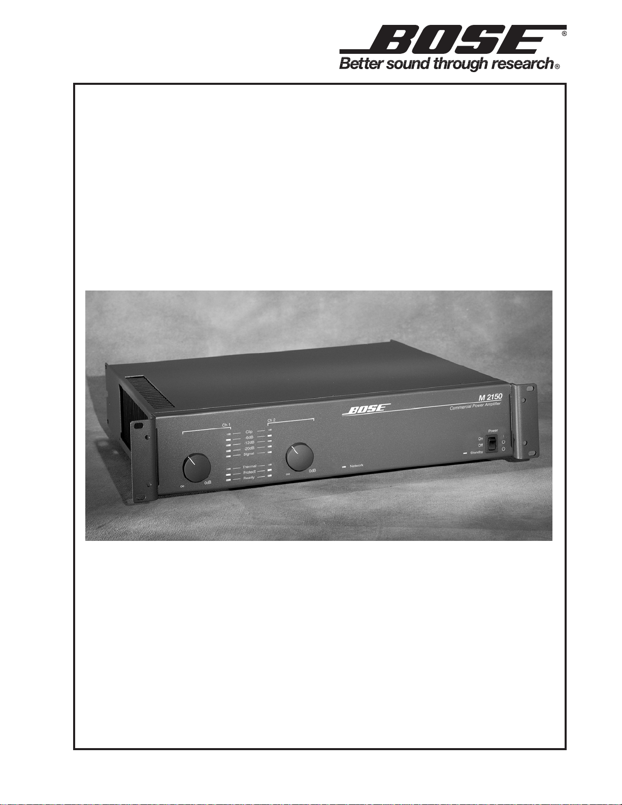
Model 2150
Commercial Power Amplifier
©2008 Bose Corporation
Service Manual
Part Number 216306 Rev . 01
Page 2

CONTENTS
Safety Information.............................................................................................................................3
Electrostatic Discharge Sensitive (ESDS) Device Handling....................................................... 3
Warranty .............................................................................................................................................3
Specifications................................................................................................................................ 4-5
Amplifier/Driver Board Version Information ...................................................................................6
Packaging Part List, Model 2150 Amplifier .....................................................................................6
Part List Notes ..................................................................................................................................7
Main Part List, Model 2150 Amplifier (items not shown on a part drawing) ................................7
Main Part List (Continued), Model 2150 Amplifier (see Figure 1)................................................8
Figure 1. Model 2150 Amplifier Top Cover Removal Exploded View....................................................8
Main Part List (Continued), Model 2150 Amplifier (see Figure 2)................................................9
Figure 2. Model 2150 Amplifier Internal Assemblies Exploded V iew ..................................................10
Main Part List (Continued), Model 2150 Amplifier (see Figure 3).............................................. 11
Figure 3. Model 2150 Amplifier Module Exploded V iew...................................................................... 11
Electrical Part Lists .................................................................................................................. 12-45
Input Module Assembly ............................................................................................................ 12-14
Barrier PCB Assembly (p art of Input Module Assembly) ............................................................15
Amplifier PCB Assembly (board p art number 6000.0435)...................................................... 16-20
Amplifier PCB Assembly (board p art number 8005.0587)...................................................... 21-26
Power Supply PCB Assembly .................................................................................................. 27-29
Switch PCB Assembly............................................................................................................... 30-31
AC Input/Output PCB Assembly.....................................................................................................32
Interface PCB Assembly........................................................................................................... 33-34
Digital Signal Processor (DSP) PCB Assembly ..................................................................... 35-43
Display PCB Assembly.............................................................................................................. 44-45
Disassembly Procedures ......................................................................................................... 46-49
Test Procedures ....................................................................................................................... 50-54
Figure 4. Model 2150 amplifier rear panel .........................................................................................50
Figure 5. Test Setup Diagram ...........................................................................................................50
Figure 6. Model 2150 Amplifier Signal Flow Block Diagram ..............................................................55
Theory of Operation ................................................................................................................. 56-65
Circuit Board Layout Diagrams ............................................................................................... 66-73
Integrated Circuit Diagrams .................................................................................................... 74-78
Troubleshooting .............................................................................................................................79
Service Manual Revision History .................................................................................................80
CAUTION: The Bose® Model 2150 amplifier contains no
user-serviceable parts. To prevent warranty infractions,
refer servicing to warranty service stations or factory service.
PROPRIETARY INFORMATION
THIS DOCUMENT CONTAINS PROPRIETARY INFORMATION OF
BOSE CORPORATION WHICH IS BEING FURNISHED ONLY FOR
THE PURPOSE OF SERVICING THE IDENTIFIED BOSE PRODUCT
BY AN AUTHORIZED BOSE SERVICE CENTER OR OWNER OF THE
BOSE PRODUCT, AND SHALL NOT BE REPRODUCED OR USED
FOR ANY OTHER PURPOSE.
2
Page 3

SAFETY INFORMATION
1. Parts that have special safety characteristics are identified by the symbol on schematics
or by special notes on the parts list. Use only replacement parts that have critical characteristics
recommended by the manufacturer.
2. Make leakage current or resistance measurements to determine that exposed parts are
acceptably insulated from the supply circuit before returning the unit to the customer .
Use the following checks to perform these measurements:
A. Leakage Current Hot Check-With the unit completely reassembled, plug the AC line cord
directly into a 120V AC outlet. (Do not use an isolation transformer during this test.) Use a leakage current tester or a metering system that complies with American National Standards Institute
(ANSI) C101.1 "Leakage Current for Appliances" and Underwriters Laboratories (UL) UL6500 /
UL60065 / IEC 60065 paragraph 9.1.1. With the unit AC switch first in the ON position and then in
OFF position, measure from a known earth ground (metal waterpipe, conduit, etc.) to all exposed metal parts of the unit (antennas, handle bracket, metal cabinet, screwheads, metallic
overlays, control shafts, etc.), especially any exposed metal parts that offer an electrical return
path to the chassis. Any current measured must not exceed 0.5 milliamp. Reverse the unit
power cord plug in the outlet and repeat test. ANY MEASUREMENTS NOT WITHIN THE LIMITS
SPECIFIED HEREIN INDICA TE A POTENTIAL SHOCK HAZARD THA T MUST BE ELIMINA TED
BEFORE RETURNING THE UNIT TO THE CUSTOMER.
B. Insulation Resistance Test Cold Check-(1) Unplug the power supply and connect a jumper
wire between the two prongs of the plug. (2) Turn on the power switch of the unit. (3) Measure
the resistance with an ohmmeter between the jumpered AC plug and each exposed metallic
cabinet part on the unit. When testing 3 wire products, the resistance measured to the product
enclosure should be between 2 and infinite MOhms. Also, the resist ance measured to exposed
input/output connectors should be between 4 and infinite MOhms. When testing 2 wire products,
the resistance measured to exposed input/output connectors should be between 4 and infinite
MOhms. If it is not within the limits specified, there is the possibility of a shock hazard, and the
unit must be repaired and rechecked before it is returned to the customer .
ELECTROSTATIC DISCHARGE SENSITIVE (ESDS)
DEVICE HANDLING
This unit contains ESDS devices. We recommend the following precautions when repairing,
replacing or transporting ESDS devices:
• Perform work at an electrically grounded work station.
• Wear wrist straps that connect to the station or heel straps that connect to conductive
floor mats.
• Avoid touching the leads or contacts of ESDS devices or PC boards even if properly
grounded. Handle boards by the edges only .
• Transport or store ESDS devices in ESD protective bags, bins, or totes. Do not insert
unprotected devices into materials such as plastic, polystyrene foam, clear plastic bags,
bubble wrap or plastic trays.
WARRANTY
The Bose® Model 2150 amplifier is covered by a five-year, transferable, limited warranty.
3
Page 4

SPECIFICATIONS
Power Output, continuous average output power, both channels driven:
150W per channel into 4 or 8 Ohms at 1kHz with 0.5% or less THD
150W per channel at 100V into a 67 Ohm load at 1 kHz with 0.5% or less THD
150W per channel at 70V into a 33 Ohm load at 1 kHz with 0.5% or less THD
Power Output, bridged-mono operation:
300W at 8 or 16 Ohms with 0.5% or less THD
300W at 100V into a 33 Ohm load with 0.5% or less THD
300W at 70V into a 16 Ohm load with 0.5% or less THD
Power Consumption:
60W or less at idle, no input, maximum gain
125W with musical program at 1/8 rated power
250W with musical program at 1/3 rated power
300W at 70V into a 41 Ohm load with 0.5% or less THD
600W at 4 Ohms with a sinewave test tone, rated continuous power at maximum gain
575W at 8 Ohms with a sinewave test tone, rated continuous power at maximum gain
560W at 70V or 100V with a sinewave test tone, rated continuous power at maximum gain
Power Requirements: 120 V AC, 60 Hz +/-20% (US and Canada)
230 V AC, 50 Hz +/-20% (Europe/UK)
240 V AC, 50 Hz +/-20% (Australia)
Output Configurations: Audio output transfomer taps per channel:
100V, 70V, 50V, 35V, 25V, 8 Ohms, 4 Ohms
Frequency Response: 30 Hz to 20 kHz (-3 dB)
Signal to Noise Ratio: > 95 dB, A-W eighted below full bandwid th power
Channel Separation: > 80 dB at 1 kHz
CMRR: > 80 dB at 1 kHz (without Bose
Slew Rate: > 10V/uSec
Sensitivity: 0.775 Vrms for rated power at 1 kHz
Input Impedance: 50k Ohms balanced, 25k Ohms unbalanced
Maximum Input: +20 dBu (7.75V)
Fusing/Protection: Mains internally fused. Amplifier thermal and
short circuit protection
®
input module)
Dynamic Headroom: 1.2 dB
Full Power Bandwidth: 30 Hz to 20 kHz at 0.5% THD
IM Distortion: 0.2%
THD: < 0.5% rated power, < 0.2% 1/8 rated power
4
Page 5

SPECIFICATIONS
Description Product Code Voltage
Features:
• Convection Cooling
• 5-segment LED level display, per channel, including signal present and clip indicators
• 3 LED display, per channel, of power, protect and thermal overload
• St andby LED indicates the amplifier is in st andby mode
• Data LED (used with the Bose
• Level controls can be covered with caps (supplied) to prevent tampering
• Remote control of output level via Euro style connectors
• S tandard Dual Input Module with line level input s via Euro style connectors and XLR jacks,
connected in parallel
• 26 Hz High Pass Filter
• Switched 80 Hz / 120 Hz (12 dB / Octave cut) High Pass Filters
• Switched Clip Limiters
• Terminals for Sequencing Power ON/OFF
• Speaker Output via large gauge Euro style connectors (accept s 12 gauge wire)
• Power Switch, 3 positions, On, Off and Standby
• AC Line Cord (Detachable IEC Type)
• Optional Accessories:
- Computer Control and Monitoring via Bose ACM-1 amplifier control module
®
ACM-1 amplifier control module)
Physical Characteristics:
Cooling Method: Convection
Operating Environment: -10 deg C up to 55 deg C, up to 85% RH
Storage Environment: -45 deg C up to 70 deg C, up to 85% RH
Dimensions: 3.5" H (2U) x 19.0" W x 16" D
8.9cm x 48.3cm x 40.6cm
Net Weight: 43 lbs. / 19.5 kgs.
Shipping Weight: 48 lbs. / 21.8 kgs.
Regulatory Information: United States: UL6500, Canada: CAN/CSA
E60065, Europe: EN 60065, Australia/New
Zealand: AS/NZS 3250, Eastern Europe, Far
East, Pacific Rim, Americas and others: IEC
60065 + CB Scheme Certification (Worldwide)
MODEL 2150 AMPLIFIER VERSIONS
Model 2150 Amplifier, Japan 025985 100V
Model 2150 Amplifier, US/Canada 025986 120V
Model 2150 Amplifier, Euro 025987 220V
Model 2150 Amplifier, UK 025988 230V
Model 2150 Amplifier, Aus 025989 240V
5
Page 6

Item
Description Vendor Part
®®®®
Qty. Note
AMPLIFIER/DRIVER BOARD VERSION INFORMATION
Units built before June 2005 have the original version of the amplifier PCB assembly . Unit s built
after that date have a different version of the amplifiier PCB assembly. Units built before June
2005 use amplifier bare board part number 6000.0435. Units built after that date use bare board
part number 8005.0587. The amplifier driver modules for these boards are different as well. The
original version used the black TAO103 module. Newer versions use a PCB assembly with a
heatsink visible on the top of the board. See below .
CAUTION: The driver modules and the amplifier boards used with them are NOT compatible
with the other versions. Any attempt s to use an incorrect driver module on an incomp atible
amplifier board will result in damage to both. Be sure to use the appropriate schematic, board
layout diagram and parts list for the amplifier PCB assembly in your unit.
Original Version Driver Module, used with
the 6000.0435 Amplifier PCB
Newer Version Driver Module, used with the
8005.0587 Amplifier PCB
PACKAGING PART LIST
Model 2150 Amplifier
Bose
Number
- Bag, Plastic, 24x30
Pack amp in bag for shipment
- Bag, Poly, 10x16x4mil 8300.0023 1
- Bag, Poly, 4x6x4mil 8300.0046 1
- Foam, Corner, 2U 8700.0060 262193 4
- Carton, 2U, 23 1/4x7 1/2x20 1/8 862003 262119 1
- Manual, Owners, DK/DE/IT/ND/SW
Model 2060/2150
- Manual, Owners, EN/ FR/ SP, Model
2060/2150
- Declaration of Conformity, Bose 2150
amplifier
- Line Cord, 120V, S250AH 4150.0009 262099 1 US/CSA
- Line Cord, MOD, 3x1.0mm, 10A,
250V
- Line Cord, MOD, 3x1.0mm, 13A,
250V
- Line Cord, MOD, 3x1.0mm, 10A,
250V
- Plug, .500, Black (covers level control
shafts after knob removal)
- Foot, Rubber, BLK, .81 sq x .3 h 5740.0006 199779 4
Number
8300.0024 1
8100.0218 262210 1 EURO
8100.0219 262194 1 US/CSA
8110.0012A 262318 1 EURO
4150.0015 262117 1 AUS
4150.0016 262118 1 UK
4150.0017 262083 1 EURO
5815.0002 262319 2
Part
Number
/EURO/
UK/AUS
3
3
3
3
6
Page 7

PART LIST NOTES
Item
Description Vendor Part
®®®®
Qty. Note
1. This part is not normally available from Customer Service. Approval from the Field Service
Manager is required before ordering.
2. The individual parts located on the PCBs are listed in the Electrical Part List.
3. This part is critical for safety purposes. Failure to use a substitute replacement with the
same safety characteristics as the recommended replacement part might create shock, fire
and/or other hazards.
4. This part is referenced for informational purposes only. It is not stocked as a repair part.
MAIN PART LIST
Model 2150 Amplifier (items not shown on a p art drawing)
Bose
Number
- Fuse, MDA, 8A, 250V, US/CSA
(F100 mains fuse)
- Fuse, MDA, 4A, 250V,
EURO/UK/AUS (F100 mains fuse)
- Conn, Plug, Term Block, 4 Pos, Blk
(ch1, ch2 EFX loop, remote level
connectors)
- Conn, Plug, Term Block, 3 Pos, Blk
(ch1, ch2 euroblock signal input,
power sequence connectors)
- Conn, Term Plug, Cbl Mt, 8 Pos
(ch1, ch2 speaker output connectors)
- Conn, .100 CTR, 2-Pin 160-20013-00 262317 1
- Cable, IDC, PLG/HDR, 20 Conductor,
- Harness, 2P, 22 AWG, Blind Mate
- Screw, SEMS, PHP, 6-32x1/4, BO,
16 inch (signal processor J101)
(input module power cable)
WAX (attach barrier pcb to input
module plate)
Number
315-13003-00 262208 1 3
4605.0001 262209 1 3
4227.0002 262104 3
4227.0008 262105 3
4227.0026 262106 2
4148.0017 262182 1
550-10087-01 182920 1
151-30169-01 262115 2 4
Part
Number
7
Page 8
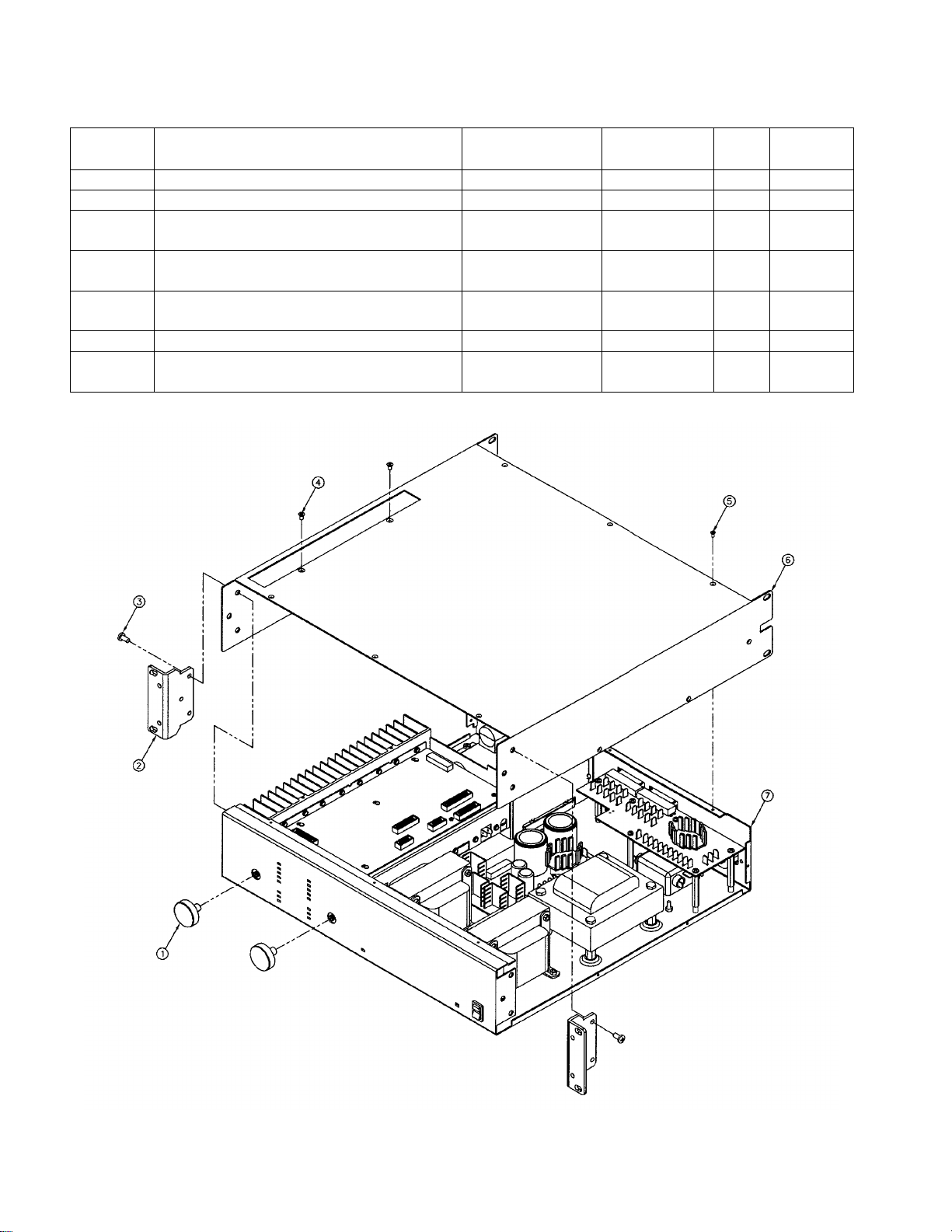
MAIN PART LIST (CONTINUED)
Item
Description Vendor Part
®®®®
Qty. Note
Model 2150 Amplifier (see Figure 1)
Bose
Number
1 Knob, Control, 1.18 OD x .5 DP Stem 5710.0001 262101 2
2 Rack Ear, 2U, Carver, Gray 700362.30 262120 2
3 Screw, SEMS, BLK OX, PHP, 10-
32x3/8
4 Screw, TF, 6-32x1/4, FHP, UC, ST,
BZ
5 Screw, TF, 4-40x1/4, FHP, UC, ST,
BZ
6 Cover, 2U, Bose 2060/2150 700487.30 262102 1
7 Amplifier Chassis Assembly
(refer to Figure 2)
Number
151-30170-01 262109 6 4
5113.0037 262113 2 4
5112.0026 199771 12 4
1
Part
Number
Figure 1. Model 2150 Amplifier Top Cover Removal Exploded View
8
Page 9

MAIN PART LIST (CONTINUED)
Item
Description Vendor Part
®®®®
Qty. Note
Model 2150 Amplifier (see Figure 2)
Bose
Number
1 Screw, TF, 6-32x1/4, FHP, UC, ST,
BZ
2 Amplifier Assembly (refer to Figure 6) 1
3 Nut, Mini STZ, 4-40 152-50004-00 182729 4 4
4 Screw, Mach, BLK OX, PHP, 4-40x1/2 151-20010-05 182717 6 4
5 Slide, Chassis, Input Module Card 159-60003-01 182731 2
6 Shield, Input Module, CV 700490 262103 1
7 Screw, TF, 4-40x1/4, FHP, UC, ST,
8 Screw, Sht Mtl, BLK OX, PHP, SERR,
9 Panel, I/O, SS, Gray, 1800V 700191.3001 199786 1 4
10 Input PCB Assembly 602-00603-02 262316 1 2
10 Barrier PCB Assembly
11 Screw, MA, 6-32x1/4, PHP, WSHR,
12 Interface PCB Assembly, CV, Dual 9000.0445.02 262086 1 2
13 AC Input/Output PCB Assembly 9000.0440.01 262085 1 2
14 Standoff, HX, M/F, 6-32x1-3/4x1/4, AL
15 Switch PCB Assembly 9000.0439.02 262084 1 2
16 Nut, 6-32, Hex, Kep, STZ 5223.0001 199774 12 4
17 Transformer, Output, 150W, CV 4554.0041 262096 2 3
18 Receptacle, IEC AC Power, Panel19 Line Filter, 16A/20A 615-00003-00 182763 1 3
20 Screw, Machine, 6-32x5/16, FHP,
21 Transformer, Power, CV, 43V/5.4A,
21 Transformer, Power, CV, 43V/5.4A,
22 Screw, SEMS, MA, 8-32x1/4, PHP,
23 Chassis, 2U, 2060/2150 700488.3001 262089 1 4
24 Switch, Rocker, Power, SPDT
25 Power Supply PCB Assembly 9000.0437.03 262082 1 2
26 Display PCB Assembly, Dual 9000.0448.02 262088 1 2
27 Nut, 4-40, Hex, Kep, STZ 5222.0001 262116 3 4
BZ
6x1/4
(part of input module)
STZ
Mount
BLK
120V (US/CSA)
230V (EURO/UK/AUS)
STBZ
ON-OFF-ON (S100)
Number
5113.0037 262113 4 4
5112.0026 199771 14 4
151-30107-01 262108 4 4
602-00533-02 182774 1 2
5113.0006 262112 18 4
5533.0046 262107 6 4
4202.0003 262093 1 3
2 4
4554.0044 262097 1 3
4554.0042 262098 1 3
5114.0012 262114 4 4
4360.0006 262095 1 3
Part
Number
9
Page 10

Figure 2. Model 2150 Amplifier Internal Assemblies Exploded View
10
Page 11
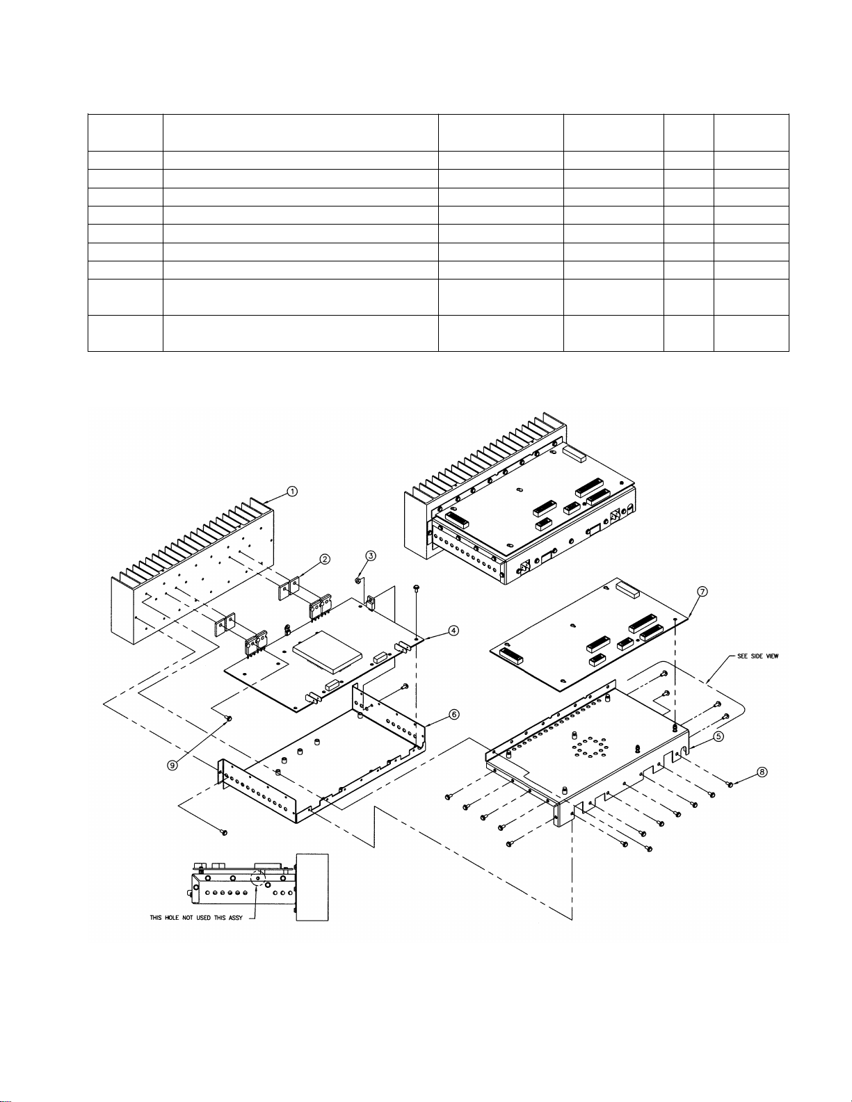
MAIN PART LIST (CONTINUED)
Item
Description Vendor Part
®®®®
Qty. Note
Model 2150 Amplifier (see Figure 3)
Bose
Number
1 Heatsink, 2U, CV 720069.31 262092 1
2 Insulator, Aluminum Oxide, TO-220 3299.0005 262100 4
3 Nut, 4-40, Hex, Kep, STZ 5222.0001 262116 1 4
4 Amplifier PCB Assembly 9000.0435.03 262081 1 2
5 Cover, Shield, Amp, CV (top) 700507 262090 1
6 Chassis, Shield, Amp, CV (bottom) 700508 262091 1
7 Signal Processor PCB Assembly 9000.0447.03 262087 1 2
8 Screw, TF, SEMS, 4-40x3/8, HWH,
ST, BZ
9 Screw, TF, SEMS, 4-40x1/2, HWH,
ST, BZ
Number
5112.0034 262111 48 4
5112.0031 262110 4 4
Part
Number
Figure 3. Model 2150 Amplifier Module Exploded View
11
Page 12

ELECTRICAL PART LIST
Reference
Description Vendor Part
®®®®
Note
Input Module Assembly
Resistors
Bose
Designator
R52 332k, MF, 1/4W, 1% 1226.3323 183000 4
R53 332k, MF, 1/4W, 1% 1226.3323 183000 4
R54 332k, MF, 1/4W, 1% 1226.3323 183000 4
R55 332k, MF, 1/4W, 1% 1226.3323 183000 4
R56 120 Ohm, CF, 1/4W, 5% 1224.0121 182995 4
R57 10k, CF, 1/4W, 5% 1224.0103 182789 4
R58 10k, CF, 1/4W, 5% 1224.0103 182789 4
R59 120k, CF, 1/4W, 5% 1224.0124 182996 4
R60 332k, MF, 1/4W, 1% 1226.3323 183000 4
R61 10k, CF, 1/4W, 5% 1224.0103 182789 4
R62 332k, MF, 1/4W, 1% 1226.3323 183000 4
R63 330 Ohm, CF, 1/4W, 5% 1224.0331 182998 4
R64 10k, CF, 1/4W, 5% 1224.0103 182789 4
R65 30k, CF, 1/4W, 5% 1224.0303 182852 4
R66 51 Ohm, CF, 1/4W, 5% 1224.0510 4
R69 10k, CF, 1/4W, 5% 1224.0103 182789 4
R70 10k, CF, 1/4W, 5% 1224.0103 182789 4
R72 100k, CF, 1/4W, 5% 1224.0104 182790 4
R73 47k, CF, 1/4W, 5% 1224.0473 182928 4
R74 47k, CF, 1/4W, 5% 1224.0473 182928 4
R75 47k, CF, 1/4W, 5% 1224.0473 182928 4
R76 10k, CF, 1/4W, 5% 1224.0103 182789 4
R77 10k, CF, 1/4W, 5% 1224.0103 182789 4
R78 47k, CF, 1/4W, 5% 1224.0473 182928 4
R79 100k, CF, 1/4W, 5% 1224.0104 182790 4
R80 47k, CF, 1/4W, 5% 1224.0473 182928 4
R81 47k, CF, 1/4W, 5% 1224.0473 182928 4
R82 47k, CF, 1/4W, 5% 1224.0473 182928 4
R83 47k, CF, 1/4W, 5% 1224.0473 182928 4
R84 300 Ohm, CF, 1/4W, 5% 1224.0301 182997 4
R85 100 Ohm, CF, 1/4W, 5% 1224.0101 182994 4
R86 390 Ohm, CF, 1/4W, 5% 1224.0391 182951 4
R87 300 Ohm, CF, 1/4W, 5% 1224.0301 182997 4
R88 100 Ohm, CF, 1/4W, 5% 1224.0101 182994 4
R89 390 Ohm, CF, 1/4W, 5% 1224.0391 182951 4
Number
Part
Number
12
Page 13
ELECTRICAL PART LIST
Reference
Description Vendor Part
®®®®
Note
Reference
Description Vendor Part
Bose Part
Note
Input Module Assembly
Designator
Capacitors
Bose
Number
Part
Number
C37 330pF, Cer Disc, COG, 100V, 5% 2174.0331 182992 4
C38 330pF, Cer Disc, COG, 100V, 5% 2174.0331 182992 4
C39 330pF, Cer Disc, COG, 100V, 5% 2174.0331 182992 4
C40 330pF, Cer Disc, COG, 100V, 5% 2174.0331 182992 4
C41 3300pF, Cer Disc, 100V, 10% 201-00133-00 183883 4
C42 3300pF, Cer Disc, 100V, 10% 201-00133-00 183883 4
C43 220uF, AE, RDL, 16V, 20% 205-00017-00 182993 4
C44 .1uF, CRML, X7R, 100V, 5mm, 20% 2175.0104 199761 4
C45 .1uF, CRML, X7R, 100V, 5mm, 20% 2175.0104 199761 4
C46 .1uF, CRML, X7R, 100V, 5mm, 20% 2175.0104 199761 4
C47 .1uF, CRML, X7R, 100V, 5mm, 20% 2175.0104 199761 4
C57 .01uF, CRML, Rdl, 100V, +80/-20% 201-00068-00 182780 4
C58 .01uF, CRML, Rdl, 100V, +80/-20% 201-00068-00 182780 4
C59 .001uF, PE, RDL, 100V, 10% 2458.0102 182839 4
C60 .01uF, CRML, Rdl, 100V, +80/-20% 201-00068-00 182780 4
C61 .01uF, CRML, Rdl, 100V, +80/-20% 201-00068-00 182780 4
C62 .001uF, PE, RDL, 100V, 10% 2458.0102 182839 4
Diodes
Designator
D1 1N4004, 400V 3100.0017 182811
D2 1N4148 3100.0004 182868
D3 1N4148 3100.0004 182868
D4 1N4004, 400V 3100.0017 182811
D5 1N4004, 400V 3100.0017 182811
D6 1N4148 3100.0004 182868
D7 1N4148 3100.0004 182868
D8 1N4148 3100.0004 182868
D9 1N4148 3100.0004 182868
D10 1N4148 3100.0004 182868
D15 Zener, 1N4764A, 18V, 1W 320-30037-02 183003
D16 1N4148 3100.0004 182868
D17 1N4148 3100.0004 182868
D18 Zener, 1N4764A, 18V, 1W 320-30037-02 183003
D20 1N4148 3100.0004 182868
D21 1N4148 3100.0004 182868
D22 1N4004, 400V 3100.0017 182811
D23 LED, Bi-Level, GRN/GRN 320-40010-01 182913
D24 1N4148 3100.0004 182868
D25 1N4148 3100.0004 182868
D26 1N4148 3100.0004 182868
D27 1N4148 3100.0004 182868
D28 1N4148 3100.0004 182868
D29 1N4148 3100.0004 182868
D30 1N4148 3100.0004 182868
D31 1N4148 3100.0004 182868
Number
Number
13
Page 14
ELECTRICAL PART LIST
Reference
Description Vendor Part
®®®®
Note
Reference
Description Vendor Part
Bose Part
Note
Reference
Description Vendor Part
Bose Part
Note
Input Module Assembly
Transistors
Part
Number
Designator
Bose
Number
Q1 NPN, MPSA06, TO-92 3200.0026 182874
Q2 PNP, MPSA56, TO-92 3200. 0003 182875
Q3 PNP, MPSA56, TO-92 3200. 0003 182875
Designator
Integrated Circuits
Number
Number
U1 Balanced Line Receiver, SSM2141 3510.2141 183005
U2 Balanced Line Receiver, SSM2141 3510.2141 183005
U3 OP-AMP W/Switch, NJM2120L 330-30062-01 183004
U4 OP-AMP W/Switch, NJM2120L 330-30062-01 183004
U5 OP-AMP W/Switch, NJM2120L 330-30062-01 183004
U6 OP-AMP W/Switch, NJM2120L 330-30062-01 183004
U7 OP-AMP, Dual, NJM072, DIP 3410. 0004 262124
Designator
Miscellaneous
Number
Number
SW1 Switch, Slide, DPTT, Right Angle 4340.0018 183002
S2 Switch, Slide, DPDT 318-40004-00 183001
P1 Jack, XLR/TRS, Right Angle 4250.0010 262125 4
P2 Phone Jack, ¼”, PC Mount 109-20002-01 182985
P3 Phone Jack, ¼”, PC Mount 109-20002-01 182985
P4 Jack, XLR/TRS, Right Angle 4250.0010 262125 4
J1 Hdr, 20 Position, Dual Row, .1 CTR 160-30051-10 182988
J2 Hdr, 4 Pos, Rt Angle, Blind Mate 160-30066-04 182991
J3 Hdr, 2 Pos, .1 CTR, Lock, ST Post 4205.0041 182921
J4 Hdr, 90 Deg, Closed End, 3 Pin 160-30064-03 182990 4
J5 Hdr, 90 Deg, Closed End, 3 Pin 160-30064-03 182990 4
J6 Hdr, 12 Pin, .098 Ctr, Shroud 160-30046-12 182987
J7 Hdr, 12 Pin, .098 Ctr, Shroud 160-30046-12 182987
JB1 Hdr, 6 Pos, Dual Row, .1 CTR, Gold 160-30054-03 182989
JB2 Hdr, 6 Pos, Dual Row, .1 CTR, Gold 160-30054-03 182989
- Conn, Mini-Link, .10”
160-20007-00 182986 Qty. 4
(used with JB1 and JB2)
- Screw, TF, 4-20x5/16, PHP, ST, BZ 5147.3202 4
14
Page 15
ELECTRICAL PART LIST
Reference
Description Vendor Part
®®®®
Note
Barrier PCB Assembly (p art of Input Module Assembly)
Bose
Designator
E1 Harness, Conn, 2 Position, 22 AWG,
3.5 in.
E2 Harness, Conn, 2 Position, 22 AWG,
3.5 in.
J2 Terminal Block, 2 Position, .15” CTR,
Angled
- Standoff, .25 OD, 6-32x.125, SWG,
BRS
- Standoff, Clinch, Keyhole, .25H 5533.0031 262123 4, Qty. 4
Number
550-10083-01 262121 4
550-10083-01 262121 4
101-00112-02 182967 4
118-80031-01 182828 4, Qty. 2
Part
Number
15
Page 16
ELECTRICAL PART LIST
Reference
Description Vendor Part
®®®®
Note
Amplifier PCB Assembly (board p art number 6000.0435)
Resistors
Bose
Designator
RT600 Thermistor, PTC, 2.2k 1200.0001 262126
R600 2. 7k , CF, 1/8W , 5% 1124.0272 4
R601 10 Ohm, MF, 1/4W, 5% 1204.0100 182937 4
R602 100k, MF, 1/8W, 1% 1126.1003 4
R603 100k, MF, 1/8W, 1% 1126.1003 4
R604 1. 00 MEG, MF, 1/8W, 1% 1126.1004 4
R605 100k, MF, 1/8W, 1% 1126.1003 4
R606 100k, MF, 1/8W, 1% 1126.1003 4
R607 1. 00 MEG, MF, 1/8W, 1% 1126.1004 4
R608 10.0k, MF, 1/8W, 1% 1126.1002 4
R609 10.0k, MF, 1/8W, 1% 1126.1002 4
R612 10.0k, MF, 1/8W, 1% 1126.1002 4
R613 10.0k, MF, 1/8W, 1% 1126.1002 4
R614 15.4k, MF, 1/8W, 1% 1126.1542 4
R615 15.4k, MF, 1/8W, 1% 1126.1542 4
R616 100k, MF, 1/8W, 1% 1126.1003 4
R617 100k, MF, 1/8W, 1% 1126.1003 4
R618 0.01 Ohm, WW, 2W, 1% 1536.0107 262127
R619 0.01 Ohm, WW, 2W, 1% 1536.0107 262127
R620 0.01 Ohm, WW, 2W, 1% 1536.0107 262127
R621 0.01 Ohm, WW, 2W, 1% 1536.0107 262127
R622 100k, MF, 1/8W, 1% 1126.1003 4
R623 100k, MF, 1/8W, 1% 1126.1003 4
R624 4.7 Ohm, MF, Fuse, 1/4W, 5% 1204.0479 182808 3
R625 4.7 Ohm, MF, Fuse, 1/4W, 5% 1204.0479 182808 3
R626 4.7 Ohm, MF, Fuse, 1/4W, 5% 1204.0479 182808 3
R627 4.7 Ohm, MF, Fuse, 1/4W, 5% 1204.0479 182808 3
R628 1. 00 MEG, MF, 1/8W, 1% 1126.1004 4
R629 1. 00 MEG, MF, 1/8W, 1% 1126.1004 4
R634 29.4k, MF, 1/8W, 1% 1126.2942 4
R639 1k, MOF, 1W, 5% 1444.0102 262142
R640 1k, MOF, 1W, 5% 1444.0102 262142
R641 27 Ohm, MOF, 2W, 5% 1544. 0270 262298
R642 27 Ohm, MOF, 2W, 5% 1544. 0270 262298
R643 10 Ohm, MF, 1/4W, 5% 1204.0100 182937 4
R644 10 Ohm, MF, 1/4W, 5% 1204.0100 182937 4
R645 10.0k, MF, 1/8W, 1% 1126.1002 4
R646 .02 Ohm, WW, 5W, 5% 1734.0207 182935
R647 .02 Ohm, WW, 5W, 5% 1734.0207 182935
R648 29.4k, MF, 1/8W, 1% 1126.2942 4
R649 10 Ohm, MF, 1/4W, 5% 1204.0100 182937 4
Number
Part
Number
16
Page 17
ELECTRICAL PART LIST
Reference
Description Vendor Part
®®®®
Note
Reference
Description Vendor Part
Bose Part
Note
Amplifier PCB Assembly (board p art number 6000.0435)
Resistors (continued)
Bose
Designator
R650 10 Ohm, MF, 1/4W, 5% 1204.0100 182937 4
R651 0 Ohm, 1/8W 1124.0000 4
R652 0 Ohm, 1/8W 1124.0000 4
R653 10 Ohm, MF, 1/4W, 5% 1204.0100 182937 4
R654 10.0k, MF, 1/8W, 1% 1126.1002 4
R655 5.11k, MF, 1/8W, 1% 1126.5111 4
R656 51. 1 Ohm, MF, 1/8W, 1% 1126.5119 4
R657 0 Ohm, 1/8W 1124.0000 4
R658 0 Ohm, 1/8W 1124.0000 4
R659 0 Ohm, 1/8W 1124.0000 4
Designator
C601 100pF, Cer Disc, NPO, 100V, 5% 2174.0101 4
C602 100pF, Cer Disc, NPO, 100V, 5% 2174.0101 4
C603 100pF, Cer Disc, NPO, 100V, 5% 2174.0101 4
C604 . 1uF, CRML, X7R, 100V, 5mm, 20% 2175.0104 199761
C605 100pF, Cer Disc, NPO, 100V, 5% 2174.0101 4
C606 22uF, AE, RDL, LOW Z, 63V, 20% 2935.0226 4
C607 100pF, Cer Disc, NPO, 100V, 5% 2174.0101 4
C608 100pF, Cer Disc, NPO, 100V, 5% 2174.0101 4
C609 100pF, Cer Disc, NPO, 100V, 5% 2174.0101 4
C610 100pF, Cer Disc, NPO, 100V, 5% 2174.0101 4
C611 100pF, Cer Disc, NPO, 100V, 5% 2174.0101 4
C612 100pF, Cer Disc, NPO, 100V, 5% 2174.0101 4
C613 100pF, Cer Disc, NPO, 100V, 5% 2174.0101 4
C614 . 47uF, MPE, 50V, 5% 2452.0474 4
C615 . 1uF, MPE, 50V, 5% 2452.0104 4
C616 . 1uF, MPE, 50V, 5% 2452.0104 4
C617 10uF, AE, RDL, 35V, 20% 2930.0106 4
C618 . 47uF, MPE, 50V, 5% 2452.0474 4
C619 . 47uF, CRML, Z5U, 50V, 5mm, 20% 2175.0474 4
C620 . 47uF, CRML, Z5U, 50V, 5mm, 20% 2175.0474 4
C621 100pF, Cer Disc, NPO, 100V, 5% 2174.0101 4
C622 . 47uF, CRML, Z5U, 50V, 5mm, 20% 2175.0474 4
C623 100pF, Cer Disc, NPO, 100V, 5% 2174.0101 4
C624 . 47uF, CRML, Z5U, 50V, 5mm, 20% 2175.0474 4
C625 . 47uF, CRML, Z5U, 50V, 5mm, 20% 2175.0474 4
C626 100uF, AE, RDL, 25V, 20% 2930.0107 4
C627 . 22uF, MPE, 50V, 5% 2452.0224 4
C628 . 22uF, MPE, 50V, 5% 2452.0224 4
C629 . 1uF, CRML, X7R, 100V, 5mm, 20% 2175.0104 199761
Capacitors
Number
Number
Part
Number
Number
17
Page 18

ELECTRICAL PART LIST
Reference
Description Vendor Part
®®®®
Note
Amplifier PCB Assembly (board p art number 6000.0435)
Capacitors (continued)
Bose
Designator
C630 . 1uF, CRML, X7R, 100V, 5mm, 20% 2175.0104 199761 4
C631 100uF, AE, RDL, 100V, 20% 2936.0107 4
C632 . 1uF, CRML, X7R, 100V, 5mm, 20% 2175.0104 199761 4
C633 100uF, AE, RDL, 100V, 20% 2936.0107 4
C634 100uF, AE, RDL, 100V, 20% 2936.0107 4
C635 . 1uF, CRML, X7R, 100V, 5mm, 20% 2175.0104 199761 4
C636 . 1uF, CRML, X7R, 100V, 5mm, 20% 2175.0104 199761 4
C637 100uF, AE, RDL, 100V, 20% 2936.0107 4
C638 . 1uF, CRML, X7R, 100V, 5mm, 20% 2175.0104 199761 4
C641 . 1uF, CRML, X7R, 100V, 5mm, 20% 2175.0104 199761 4
C642 . 1uF, CRML, X7R, 100V, 5mm, 20% 2175.0104 199761 4
C645 . 1uF, CRML, X7R, 100V, 5mm, 20% 2175.0104 199761 4
C646 100pF, Cer Disc, NPO, 100V, 5% 2174.0101 4
C651 . 1uF, MPE, 50V, 5% 2452. 0104 4
C652 . 1uF, MP, 250VAC, UL/CSA 2462.1104 182846 4
C653 . 1uF, MP, 250VAC, UL/CSA 2462.1104 182846 4
C654 . 1uF, MPE, 50V, 5% 2452.0104 4
C655 18pF, Cer Disc, NPO, 100V, 5% 2174. 0180 4
C656 18pF, Cer Disc, NPO, 100V, 5% 2174. 0180 4
C658 . 33uF, MPE, BOX, 100V, 5% 2452.2334 4
C659 . 33uF, MPE, BOX, 100V, 5% 2452.2334 4
C660 . 1uF, CRML, X7R, 100V, 5mm, 20% 2175.0104 199761 4
C661 . 1uF, CRML, X7R, 100V, 5mm, 20% 2175.0104 199761 4
C662 100pF, Cer Disc, NPO, 100V, 5% 2174.0101 4
C663 100pF, Cer Disc, NPO, 100V, 5% 2174.0101 4
C664 . 01uF, MPE, BOX, 100V, 5% 2452.2103 4
C665 . 01uF, MPE, BOX, 100V, 5% 2452.2103 4
C666 100pF, Cer Disc, NPO, 100V, 5% 2174.0101 4
C667 100pF, Cer Disc, NPO, 100V, 5% 2174.0101 4
C668 100pF, Cer Disc, NPO, 100V, 5% 2174.0101 4
C669 100pF, Cer Disc, NPO, 100V, 5% 2174.0101 4
C670 100pF, Cer Disc, NPO, 100V, 5% 2174.0101 4
C671 100pF, Cer Disc, NPO, 100V, 5% 2174.0101 4
C672 . 47uF, CRML, Z5U, 50V, 5mm, 20% 2175.0474 4
C673 100uF, AE, RDL, LOW Z, 25V, 20% 2392.0107 4
C674 100pF, Cer Disc, NPO, 100V, 5% 2174.0101 4
C675 100pF, Cer Disc, NPO, 100V, 5% 2174.0101 4
C676 . 1uF, CRML, X7R, 100V, 5mm, 20% 2175.0104 199761 4
C677 . 1uF, CRML, X7R, 100V, 5mm, 20% 2175.0104 199761 4
C678 . 1uF, CRML, X7R, 100V, 5mm, 20% 2175.0104 199761 4
C679 . 1uF, CRML, X7R, 100V, 5mm, 20% 2175.0104 199761 4
C680 100pF, Cer Disc, NPO, 100V, 5% 2174.0101 4
Number
Part
Number
18
Page 19
ELECTRICAL PART LIST
Reference
Description Vendor Part
®®®®
Note
Reference
Description Vendor Part
Bose Part
Note
Reference
Description Vendor Part
Bose Part
Note
Reference
Description Vendor Part
Bose Part
Note
Amplifier PCB Assembly (board p art number 6000.0435)
Inductors
Part
Number
Designator
Bose
Number
L600 330uH, .54A, RL622-331K 4500.0029 262128
L610 11uH, 9A, Filter 4500.0032 262129
L611 Jumper, 18 AWG, .5 inch, Insulated 401-30015-01 262130
L620 11uH, 9A, Filter 4500.0032 262129
L621 Jumper, 18 AWG, .5 inch, Insulated 401-30015-01 262130
Designator
Diodes
Number
Number
D600 1N4002 3100.0005 262192
D601 1N4002 3100.0005 262192
D602 1N5263B, Zener, 56V, .5W, 5% 3110.3630 262131
D603 MUR120 3100.0001 262132
D610 MUR120 3100.0001 262132
D611 MUR120 3100.0001 262132
D620 MUR120 3100.0001 262132
D621 MUR120 3100.0001 262132
Designator
Transistors
Number
Number
Q600 NPN, 2SC4793, TO-220FP 3200.0080 262133
Q601 PNP, 2N4403, TO-92 3200.0002 262134
Q610 N-CH MOSFET, STW34NB20 247 3210.0017 262135
Q611 N-CH MOSFET, STW34NB20 247 3210.0017 262135
Q620 N-CH MOSFET, STW34NB20 247 3210.0017 262135
Q621 N-CH MOSFET, STW34NB20 247 3210.0017 262135
Integrated Circuits
Designator
Number
Number
U600 Volt Reg, Switcher, LM2594N 3430.0009 262136
U602 Volt Reg, L7805CP, ISOWATT220 3430.0007 262137
U603 O P- AMP, Dual, NJM072, DIP 3410.0004 262124
U604 O P- AMP, Dual, NJM072, DIP 3410.0004 262124
U605 DRI VER, DIGITAL AMPLIFIER,
3440.0005 262138
TAO103A
19
Page 20
ELECTRICAL PART LIST
Reference
Description Vendor Part
®®®®
Note
Amplifier PCB Assembly (board p art number 6000.0435)
Miscellaneous
Bose
Designator
J601 Cable, I DC, PCB/PLG, 10 Cond, 4 in 4148.0018 262139
J602 Cable, I DC, PCB/PLG, 10 Cond, 4 in 4148.0018 262139
P600 Conn, Plug, HSG, 2.13mm, 4 Pin 4206.0004 262140
WL610 Conn, Tab, .250, Right Angle, PC Mnt 4200.0019 262141
WL611 Conn, Tab, .250, Right Angle, PC Mnt 4200.0019 262141
WL620 Conn, Tab, .250, Right Angle, PC Mnt 4200.0019 262141
WL621 Conn, Tab, .250, Right Angle, PC Mnt 4200.0019 262141
- Conn, Hdr, 1x8x.100, Female, 8 Pin
(sockets for U605)
- Conn, Hdr, 1x11x.100, Female, 11 Pin
(sockets for U605)
- Conn, Terminal, 2.13mm, 4 Pin
(terminals for P600)
- Heatsink, TO-220, 1.18H, Vert, PC
Mnt (Used on U602)
- Screw, MA, PHP, 4-40x3/8, BLK
(Used on U602)
- Nut, 4-40, HEX, KEP, STZ
(Used on U602)
- Grommet, 1/4ID x 9/16OD 5820.0007 262145 Qty. 1
Number
4205.0070 262320 Qty. 2
4205.0071 262143 Qty. 2
4211.0002 262144 Qty. 4
5630.0006 262155 Qty. 1
151-20002-00 262156 Qty. 1
5222.0001 262154 Qty. 1
Part
Number
20
Page 21

ELECTRICAL PART LIST
Reference
Description Bose® Part
Vendor Part
Note
Amplifier PCB Assembly (board p art number 8005.0587)
Resistors
Designator
R602 93. 1K, MF, 1/8W, 1% - 1126.9312 4
R603 93. 1K, MF, 1/8W, 1% - 1126.9312 4
R604 1. 00 MEG, MF, 1/8W, 1% - 1126.1004 4
R605 100K, MF, 1/8W, 1% - 1126.1003 4
R606 100K, MF, 1/8W, 1% - 1126.1003 4
R607 1. 00 MEG, MF, 1/8W, 1% - 1126.1004 4
R608 10. 0K, MF, 1/8W, 1% - 1126.1002 4
R609 10. 0K, MF, 1/8W, 1% - 1126.1002 4
R612 10. 0K, MF, 1/8W, 1% - 1126.1002 4
R613 10. 0K, MF, 1/8W, 1% - 1126.1002 4
R616 1. 00 MEG, MF, 1/8W, 1% - 1126.1004 4
R617 1. 00 MEG, MF, 1/8W, 1% - 1126.1004 4
R618 0.01 OHM, WW, 3W, 1% - L.1536.0107 4
R619 0.01 OHM, WW, 3W, 1% - L.1536.0107 4
R620 0.01 OHM, WW, 3W, 1% - L.1536.0107 4
R621 0.01 OHM, WW, 3W, 1% - L.1536.0107 4
R622 499K, MF, 1/8W, 1% - 1126.4993 4
R623 499K, MF, 1/8W, 1% - 1126.4993 4
R624 15 OHM, MOF, 1W, 5% - L.1444.0150 4
R625 15 OHM, MOF, 1W, 5% - L.1444.0150 4
R626 15 OHM, MOF, 1W, 5% - L.1444.0150 4
R627 15 OHM, MOF, 1W, 5% - L.1444.0150 4
R628 499K, MF, 1/8W, 1% - 1126.4993 4
R629 499K, MF, 1/8W, 1% - 1126.4993 4
R634 29. 4K, MF, 1/8W, 1% - 1126.2942 4
R639 0 OHM, 1/4W - 1224.0000 4
R640 0 OHM, 1/4W - 1224.0000 4
R641 27 OHM, MOF, 2W, 5% 262998 1544.0270
R642 27 OHM, MOF, 2W, 5% 262998 1544.0270
R643 10 OHM, MF, FUSE, 1/4W, 5% 182937 1204.0100 3
R644 10 OHM, MF, FUSE, 1/4W, 5% 182937 1204.0100 3
R645 10. 0K, MF, 1/8W, 1% - 1126.1002 4
R646 0.02OHM, WW, 5W, 5% 182935 1734.0207
R647 0.02OHM, WW, 5W, 5% 182935 1734.0207
R648 29. 4K, MF, 1/8W, 1% - 1126.2942 4
Number
Number
21
Page 22

ELECTRICAL PART LIST
Reference
Description Bose® Part
Vendor Part
Note
Reference
Description Bose Part
Vendor Part
Note
Amplifier PCB Assembly (board p art number 8005.0587)
Resistors (continued)
Designator
R649 10 O HM, MF, FUSE, 1/4W, 5% 182937 1204.0100 3
R650 10 O HM, MF, FUSE, 1/4W, 5% 182937 1204.0100 3
R651 0 OHM, 1/8W - 1124.0000 4
R652 0 OHM, 1/8W - 1124.0000 4
R653 10 O HM, MF, FUSE, 1/4W, 5% 182937 1204.0100 3
R654 10. 0K, MF, 1/8W, 1% - 1126.1002 4
R655 5. 11K, MF, 1/8W, 1% - 1126.5111 4
R656 51.1OHM, MF, 1/8W, 1% - 1126.5119 4
R660 27 O HM, MOF, 2W, 5% - 1544.0270 4
R661 27 O HM, MOF, 2W, 5% - 1544.0270 4
R666 16 O HM, MOF, 1W, 5% - L.1444.0160 4
R667 16 O HM, MOF, 1W, 5% - L.1444.0160 4
Number
Number
Capacitors
Designator
C600 220pF, CD, 10%, 1000V - L.201-0 0018-00
C601 0. 01uF, CD, 20%, 500V - L.201-00034-00
C602 0. 1uF, CRML, 20%, X7R, 100V - L.2175.0104
C603 0. 1uF, CRML, 20%, X7R, 100V - L.2175.0104
C605 0. 1uF, CRML, 20%, X7R, 100V - L.2175.0104
C607 0. 1uF, CRML, 20%, X7R, 100V - L.2175.0104
C608 0. 01uF, CD, 20%, 500V - L.201-00034-00
C609 0. 01uF, CD, 20%, 500V - L.201-00034-00
C610 0. 01uF, CD, 20%, 500V - L.201-00034-00
C611 0. 01uF, CD, 20%, 500V - L.201-00034-00
C612 0. 01uF, CD, 20%, 500V - L.201-00034-00
C613 100pF, CD, 5%, NPO, 100V - 2174.0101 4
C614 0. 47uF, MPE, 5%, 50V - L.2452.0474 4
C615 100nF, MPE, 5%, 50V - L.2452. 0104 4
C616 100nF, MPE, 5%, 50V - L.2452. 0104 4
C617 10uF, AE, RDL, 20%, 35V - 2930.0106 4
C618 0. 47uF, MPE, 5%, 50V - L.2452.0474 4
C619 0. 47uF, CRML, 20%, Z5U, 50V - L. 2175. 0474 4
Number
Number
4
4
4
4
4
4
4
4
4
4
4
22
Page 23

ELECTRICAL PART LIST
Reference
Description Bose® Part
Vendor Part
Note
Amplifier PCB Assembly (board p art number 8005.0587)
Capacitors (continued)
Designator
C620 0. 47uF, CRML, 20%, Z5U, 50V - L.2175.0474 4
C621 100pF, CD, 5%, NPO, 100V - 2174.0101 4
C622 0. 47uF, CRML, 20%, Z5U, 50V - L.2175.0474 4
C623 100pF, CD, 5%, NPO, 100V - 2174.0101 4
C624 0. 47uF, CRML, 20%, Z5U, 50V - L.2175.0474 4
C625 0. 47uF, CRML, 20%, Z5U, 50V - L.2175.0474 4
C626 100uF, AE, RDL, 20%, 25V - 2930.0107 4
C627 220nF, MPE, 5%, 50V - L.2452. 0224 4
C628 220nF, MPE, 5%, 50V - L.2452. 0224 4
C630 0. 1uF, CRML, 20%, X7R, 100V - L.2175.0104
C631 100uF, AE, RDL, 20%, 100V - L.2936.0107 4
C632 0. 1uF, CRML, 20%, X7R, 100V - L.2175.0104
C633 100uF, AE, RDL, 20%, 100V - L.2936.0107 4
C634 100uF, AE, RDL, 20%, 100V - L.2936.0107 4
C635 0. 1uF, CRML, 20%, X7R, 100V - L.2175.0104
C636 0. 1uF, CRML, 20%, X7R, 100V - L.2175.0104
C637 100uF, AE, RDL, 20%, 100V - L.2936.0107 4
C638 0. 1uF, CRML, 20%, X7R, 100V - L.2175.0104
C641 0. 1uF, CRML, 20%, X7R, 100V - L.2175.0104
C642 0. 1uF, CRML, 20%, X7R, 100V - L.2175.0104
C645 0. 1uF, CRML, 20%, X7R, 100V - L.2175.0104
C646 0. 01uF, CD, 20%, 500V - L.201-00034-00
C647 220pF, CD, 10%, 1000V - L.201-00018-00
C648 0. 1uF, CRML, 20%, X7R, 100V - L.2175.0104
C649 0. 1uF, CRML, 20%, X7R, 100V - L.2175.0104
C651 100nF, MPE, 5%, 50V - L.2452. 0104 4
C652 0. 1uF, PP, BOX, 10%, 250V - 2593.0104 4
C653 0. 1uF, PP, BOX, 10%, 250V - 2593.0104 4
C654 100nF, MPE, 5%, 50V - L.2452. 0104 4
C657 22uF, AE, 20%, 160V - 2982.0226 4
C658 0. 68uF MPP, HF, 5%, 160V - L.2574.0684 4
C659 0. 68uF MPP, HF, 5%, 160V - L.2574.0684 4
C660 0. 22uF, MPP, HF, 5%, 250V - L.2594.0224 4
C661 0. 22uF, MPP, HF, 5%, 250V - L.2594.0224 4
C662 0. 01uF, CD, 20%, 500V - L.201-00034-00
C663 0. 01uF, CD, 20%, 500V - L.201-00034-00
C664 0. 01uF, CD, 20%, 500V - L.201-00034-00
Number
Number
4
4
4
4
4
4
4
4
4
4
4
4
4
4
4
23
Page 24
ELECTRICAL PART LIST
Reference
Description Bose® Part
Vendor Part
Note
Reference
Description Bose Part
Vendor Part
Note
Amplifier PCB Assembly (board p art number 8005.0587)
Capacitors (continued)
Designator
C665 0. 01uF, CD, 20%, 500V - L.201-00034-00
C666 100pF, CD, 5%, NPO, 100V - 2174.0101 4
C667 100pF, CD, 5%, NPO, 100V - 2174.0101 4
C668 100pF, CD, 5%, NPO, 100V - 2174.0101 4
C669 0. 01uF, CD, 20%, 500V - L.201-00034-00
C670 0. 1uF, CRML, 20%, X7R, 100V - L.2175.0104
C671 100pF, CD, 5%, NPO, 100V - 2174.0101 4
C672 0. 47uF, CRML, 20%, Z5U, 50V - L. 2175. 0474 4
C674 0. 1uF, CRML, 20%, X7R, 100V - L.2175.0104
C675 0. 01uF, CD, 20%, 500V - L.201-00034-00
C676 0. 1uF, CRML, 20%, X7R, 100V - L.2175.0104
C677 0. 1uF, CRML, 20%, X7R, 100V - L.2175.0104
C678 0. 1uF, CRML, 20%, X7R, 100V - L.2175.0104
C679 0. 1uF, CRML, 20%, X7R, 100V - L.2175.0104
C680 100pF, CD, 5%, NPO, 100V - 2174.0101 4
C681 22uF, AE, 20%, 160V - 2982.0226 4
C683 0. 01uF, CD, 20%, 500V - L.201-00034-00
C684 0. 01uF, CD, 20%, 500V - L.201-00034-00
C685 0. 18uF, MPP, HF, 5%, 250V - L.2594.0184 4
C686 0. 18uF, MPP, HF, 5%, 250V - L.2594.0184 4
Number
Number
4
4
4
4
4
4
4
4
4
4
4
Inductors
Designator
L610 INDUCTOR, FILTER, 11uH, 9A - L.4500.0032 4
L611 INDUCTOR, IRON, PWDR, 7.8uH,
10A
L620 INDUCTOR, FILTER, 11uH, 9A - L.4500.0032 4
L621 INDUCTOR, IRON, PWDR, 7.8uH,
10A
FB600 FERRITE BEAD, 133 ohm at 100mHz - L.4510.0003 4
Number
- 4500.0054 4
- 4500.0054 4
Number
24
Page 25

ELECTRICAL PART LIST
Reference
Description Bose® Part
Vendor Part
Note
Reference
Description Bose Part
Vendor Part
Note
Reference
Description Bose Part
Vendor Part
Note
Reference
Description Bose Part
Vendor Part
Note
Amplifier PCB Assembly (board p art number 8005.0587)
Diodes
Designator
D600 1N4002 262192 3100.0005
D601 1N4002 262192 3100.0005
D610 SWITCHING, MUR120, AXL - L.3100.0001 4
D611 SWITCHING, MUR120, AXL - L.3100.0001 4
D614 SWITCHING, MUR120, AXL - L.3100.0001 4
D615 SWITCHING, MUR120, AXL - L.3100.0001 4
D620 SWITCHING, MUR120, AXL - L.3100.0001 4
D621 SWITCHING, MUR120, AXL - L.3100.0001 4
D624 SWITCHING, MUR120, AXL - L.3100.0001 4
D625 SWITCHING, MUR120, AXL - L.3100.0001 4
Designator
Q601 PNP, 2N4403TO-92 262134 3200.0002
Q610 N-CH FET, STW34NB20, TO-247 - L.3210.0017 4
Q611 N-CH FET, STW34NB20, TO-247 - L.3210.0017 4
Q620 N-CH FET, STW34NB20, TO-247 - L.3210.0017 4
Q621 N-CH FET, STW34NB20, TO-247 - L.3210.0017 4
Transistors
Integrated Circuits
Number
Number
Number
Number
Designator
U602 VOLT REG, L7805CP, ISOWATT 220 262137 3430.0007
U603 O P AMP, DUAL, X072, DIP 262124 3410.0004
U604 O P AMP, DUAL, X072, DIP 262124 3410.0004
Number
Number
Amplifier Driver PCB Assembly (used with amplifier board p art number 8005.0587)
Designator
U901/U902 AMPLIFIER DRIVER SET, 300W,
TRIPATH TK2350
Number
317790-001S
Number
- 3
25
Page 26

ELECTRICAL PART LIST
Reference
Description Bose® Part
Vendor Part
Note
Amplifier PCB Assembly (board p art number 8005.0587)
Miscellaneous
Designator
H1 GROMMET, 1/4 ID x 9/16 OD - 5820.0007 4
H2 GROMMET, 1/4 ID x 9/16 OD - 5820.0007 4
H3 GROMMET, 1/4 ID x 9/16 OD - 5820.0007 4
H4 GROMMET, 1/4 ID x 9/16 OD - 5820.0007 4
J601 CABLE, IDC, PCB/PLG 10, CON, 4 IN
J602 CABLE, IDC, PCB/PLG 10, CON, 4 IN
P600 CONN, PLUG, HSG, 2.13mm, 4 PIN 262140 4206.0004
RT600 THERMISTOR, PTC, 2.2k at 60 DEG
C
WL610 CONN, TAB, 0.25", RTANG, PC MNT 262141 L.4200.0019
WL611 CONN, TAB, 0.25", RTANG, PC MNT 262141 L.4200.0019
WL620 CONN, TAB, 0.25", RTANG, PC MNT 262141 L.4200.0019
WL621 CONN, TAB, 0.25", RTANG, PC MNT 262141 L.4200.0019
- CONN, HDR, 0.1" CTR, FEM, 8-SIP
(sockets for U605)
- CONN, HDR, 0.1" CTR, FEM, 11-SIP
(sockets for U605)
- CONN, TERM, 2.13mm, 14-20 AWG,
FEM (terminals for P600)
Number
262139 4148.0018
262139 4148.0018
262126 L.1200.0001
- L.4205.0070 Qty. 2
- L.4205.0071 Qty. 2
- L.4211.0002 Qty. 4
Number
26
Page 27

ELECTRICAL PART LIST
Reference
Description Vendor Part
®®®®
Note
Reference
Description Vendor Part
Bose Part
Note
Power Supply PCB Assembly
Resistors
Part
Number
Designator
Bose
Number
R400 4. 7k , MOF, 2W, 5% 1544.0472 262299
R401 2. 2k , MOF, 1W, 5% 1444.0222 262296
R402 4. 7k , MOF, 2W, 5% 1544.0472 262299
R403 2. 2k , MOF, 1W, 5% 1444.0222 262296
Designator
C400 . 1uF, MPE, 250V, 10% 2462.0104 4
C401 . 1uF, MPE, 250V, 10% 2462.0104 4
C402 . 1uF, MPE, 250V, 10% 2462.0104 4
C403 . 1uF, MPE, 250V, 10% 2462.0104 4
C404 6800uF, AE, SNAP, 63V, 30x40 2940.0688 262861
C405 2200uF, AE, RDL, 35V, 20% 2933.0228 4
C406 6800uF, AE, SNAP, 63V, 30x40 2940.0688 262861
C407 2200uF, AE, RDL, 35V, 20% 2933.0228 4
C408 . 1uF, MPE, BOX, 100V, 5% 2452.2104 4
C409 . 1uF, MPE, BOX, 100V, 5% 2452.2104 4
C410 . 1uF, MPE, BOX, 100V, 5% 2452.2104 4
C411 . 1uF, MPE, BOX, 100V, 5% 2452.2104 4
C414 . 47uF, CRML, Z5U, 5mm, 20% 2175.0474 4
C415 . 47uF, CRML, Z5U, 5mm, 20% 2175.0474 4
C416 . 47uF, CRML, Z5U, 5mm, 20% 2175.0474 4
C417 . 47uF, CRML, Z5U, 5mm, 20% 2175.0474 4
C418 100uF, AE, RDL, 25V, 20% 2930.0107 4
C419 100uF, AE, RDL, 25V, 20% 2930.0107 4
C420 10uF, AE, RDL, 35V, 20% 2930.0106 4
C422 . 47uF, CRML, Z5U, 5mm, 20% 2175.0474 4
C423 100uF, AE, RDL, 25V, 20% 2930.0107 4
C425 . 47uF, CRML, Z5U, 5mm, 20% 2175.0474 4
C444 100uF, AE, RDL, 25V, 20% 2930.0107 4
C445 . 47uF, CRML, Z5U, 5mm, 20% 2175.0474 4
C446 . 47uF, CRML, Z5U, 5mm, 20% 2175.0474 4
C447 100uF, AE, RDL, 25V, 20% 2930.0107 4
Capacitors
Number
Number
27
Page 28

ELECTRICAL PART LIST
Reference
Description Vendor Part
®®®®
Note
Reference
Description Vendor Part
Bose Part
Note
Power Supply PCB Assembly
Diodes
Bose
Designator
D400 1N4004, 400V 3100.0017 182811 3
D401 1N4004, 400V 3100.0017 182811 3
D402 Rect if ier , Bridge, 400V, 25A 3100.0025 182866 3
D403 1N4004, 400V 3100.0017 182811 3
D404 1N4004, 400V 3100.0017 182811 3
D405 1N4004, 400V 3100.0017 182811
D406 1N4004, 400V 3100.0017 182811
D407 1N4004, 400V 3100.0017 182811
D408 1N4004, 400V 3100.0017 182811
D409 1N4004, 400V 3100.0017 182811
D410 1N4004, 400V 3100.0017 182811
D411 1N4004, 400V 3100.0017 182811
D412 1N4004, 400V 3100.0017 182811
D413 1N4004, 400V 3100.0017 182811
D414 1N4004, 400V 3100.0017 182811
D415 1N4004, 400V 3100.0017 182811
Number
Part
Number
Integrated Circuits
Designator
U400 VO LT REG, +15V, NJM7815FA 3430.0005 262146
U401 VO LT REG, -15V, 7915 3430.0006 262147
U402 VO LT REG, -15V, 7915 3430.0006 262147
U403 VO LT REG, +15V, NJM7815FA 3430.0005 262146
U404 VO LT REG, +15V, NJM7815FA 3430.0005 262146
Number
Number
28
Page 29

ELECTRICAL PART LIST
Reference
Description Vendor Part
®®®®
Note
Power Supply PCB Assembly
Miscellaneous
Bose
Designator
WL400 Terminal, Quick-Connect, .250 TAB 4200.0017 262148
WL401 Terminal, Quick-Connect, .250 TAB 4200.0017 262148
WL402 Terminal, Quick-Connect, .250 TAB 4200.0017 262148
WL403 Terminal, Quick-Connect, .250 TAB 4200.0017 262148
WL404 Terminal, Quick-Connect, .250 TAB 4200.0017 262148
WL405 Terminal, Quick-Connect, .250 TAB 4200.0017 262148
P600 Conn, Hdr, Vertical, 2. 13mm, 4 Pin 4205.0064 262149
F400 10A, 125V, 5x20mm 4600.0001 262150 3
F401 10A, 125V, 5x20mm 4600.0001 262150 3
F402 2A, 250V, TL, 5x20mm 4600.0004 262151 3
F403 2A, 250V, TL, 5x20mm 4600.0004 262151 3
- Fuse Holder, Clip, 5x20mm
(Used on F400, F401, F402, F403)
- Cable, IDC, SKT/CONN, 20 COND,
6 in (install in J300)
- Nut, 4-40, HEX, KEP, STZ 5222.0001 262154 Qty. 5
- Heatsink, TO-220, 1.18H, Vert, PC
Mnt (Used with U400, U401, U402,
U403, U404)
- Heatsink, .75H, TO-3, Custom Hole
Used with D402
- Standoff, .25OD, 6-32x.187, SWG,
BRS (Used with D402)
- Screw, MA, PHP, 4-40x3/8, BLK
(Used on U400, U401, U402, U403,
U404)
- Screw, MA, PHP, 6-32X3/4, BLK
(Used on D402)
Number
4610.0011 262152 Qty. 8,
4148.0014 262153
5630.0006 262155 Qty. 4
5630.0009 199778 Qty. 1
118-80031-02 199749 Qty. 1
151-20002-00 262156 Qty. 5
151-20054-00 262157 Qty. 1
Part
Number
3
29
Page 30

ELECTRICAL PART LIST
Reference
Description Vendor Part
Bose Part
Note
Reference
Description Vendor Part
®®®®
Note
Reference
Description Vendor Part
Bose Part
Note
Reference
Description Vendor Part
Bose Part
Note
Switch PCB Assembly
Resistors
Designator
Bose
Number
Part
Number
R100 33k, MOF, 1W, 5% 1444.0333 262297 3
R101 33k, MOF, 1W, 5% 1444.0333 262297 3
Designator
C2 .01uF, Cer Disc, 250VAC, 10%,
UL/CSA
Capacitors
Number
Number
201-00035-00 3, 4
Designator
Diodes
Number
Number
D2 LED, T-1, WHT DIFF LENS, AMBER 3600.0029 262094
D3 LED, RECT, 2x5MM, YELLOW
3600.0025 262158
Standby LED
D101 1N4004, 400V 3100.0017 182811 3
Miscellaneous
Designator
- Connector, Terminal, PCMT, 1 Pos.
Mounting brackets for switch pc assy.
- Spacer, LED Standoff, .75 in.
LED standoff
30
Number
4227.0022 262159 Qty. 2
5500.0002 262160 Qty. 1
Number
Page 31

ELECTRICAL PART LIST
Reference
Description Vendor Part
®®®®
Note
Reference
Description Vendor Part
Bose Part
Note
Reference
Description Vendor Part
Bose Part
Note
Reference
Description Vendor Part
Bose Part
Note
Reference
Description Vendor Part
Bose Part
Note
AC Input/Output PCB Assembly
Resistors
Part
Number
Designator
Bose
Number
R101 1k, CF, 1/8W, 5% 1124.0102 4
R102 18 Ohm, HM, CC, 1/2W, 5% 1354.0180 187934-
18R0
3
R103 8. 2 Ohm, CF, 1/2W, 5% 1324.0829 182857 3
Designator
C100 . 10uF, MP, 250VAC, UL/CSA 2462.1104 182846 3
C101 . 10uF, MP, 250VAC, UL/CSA 2462.1104 182846 3
Designator
Capacitors
Transistors
Number
Number
Number
Number
Q100 Triac, BTA41-700B, 40 Amp, 700V 3280.0005 262161 3
Integrated Circuits
Designator
Number
Number
U100 OPTO, LED/MOSFET, PS7341-1A 3610.0008 262162 3
Designator
Miscellaneous
Number
Number
J100 Conn, Hdr, .1 CTR, 2 Pin 4205.0001 262163
J101 Conn, Hdr, HZ, FEM, .2 in, 8 Pos.
4227.0027 262164 3
(Channel 2 speaker output)
J102 Conn, Hdr, HZ, FEM, .2 in, 8 Pos.
(Channel 1 speaker output)
4227.0027 262164 3
F100 8A, 250V, MDA 315-13003-00 262165 3
- Fuse Holder, Clip, .25 Dia, PC MNT
Clips for F100
- Heatsink, .75H, TO-3, Custom Hole
4610.0008 262166 Qty. 2,
3
5630.0009 199778 Qty. 1
Heatsink for Q100
- Screw, MA, PHP, 6-32x3/8, BLK
151-20052-00 262167 Qty. 1
Attach heatsink to Q100
- Standoff, .25OD, 6-32x.187, SWG,
BRS (Used on Q100)
118-80031-02 199749 Qty. 1
31
Page 32

ELECTRICAL PART LIST
Reference
Description Vendor Part
®®®®
Note
AC Input/Output PCB Assembly
Miscellaneous (continued)
Bose
Designator
WL100 Terminal, Quick-Connect, .250 Tab 4200.0017 262148
WL101 Terminal, Quick-Connect, .250 Tab 4200.0017 262148
WL102 Terminal, Quick-Connect, .250 Tab 4200.0017 262148
WL103 Terminal, Quick-Connect, .250 Tab 4200.0017 262148
WL104 Terminal, Quick-Connect, .250 Tab 4200.0017 262148
WL105 Terminal, Quick-Connect, .250 Tab 4200.0017 262148
WL106 Terminal, Quick-Connect, .250 Tab 4200.0017 262148
WL107 Terminal, Quick-Connect, .250 Tab 4200.0017 262148
WL108 Terminal, Quick-Connect, .250 Tab 4200.0017 262148
WL109 Terminal, Quick-Connect, .250 Tab 4200.0017 262148
WL110 Terminal, Quick-Connect, .250 Tab 4200.0017 262148
WL111 Terminal, Quick-Connect, .250 Tab 4200.0017 262148
WL112 Terminal, Quick-Connect, .250 Tab 4200.0017 262148
WL113 Terminal, Quick-Connect, .250 Tab 4200.0017 262148
WL121 Terminal, Quick-Connect, .250 Tab 4200.0017 262148
WL122 Terminal, Quick-Connect, .250 Tab 4200.0017 262148
WL123 Terminal, Quick-Connect, .250 Tab 4200.0017 262148
WL124 Terminal, Quick-Connect, .250 Tab 4200.0017 262148
WL125 Terminal, Quick-Connect, .250 Tab 4200.0017 262148
WL126 Terminal, Quick-Connect, .250 Tab 4200.0017 262148
WL127 Terminal, Quick-Connect, .250 Tab 4200.0017 262148
WL128 Terminal, Quick-Connect, .250 Tab 4200.0017 262148
WL129 Terminal, Quick-Connect, .250 Tab 4200.0017 262148
WL130 Terminal, Quick-Connect, .250 Tab 4200.0017 262148
WL131 Terminal, Quick-Connect, .250 Tab 4200.0017 262148
WL132 Terminal, Quick-Connect, .250 Tab 4200.0017 262148
WL133 Terminal, Quick-Connect, .250 Tab 4200.0017 262148
WL134 Terminal, Quick-Connect, .250 Tab 4200.0017 262148
WL135 Terminal, Quick-Connect, .250 Tab 4200.0017 262148
WL136 Terminal, Quick-Connect, .250 Tab 4200.0017 262148
WL137 Terminal, Quick-Connect, .250 Tab 4200.0017 262148
WL139 Terminal, Quick-Connect, .250 Tab 4200.0017 262148
Number
Part
Number
32
Page 33

ELECTRICAL PART LIST
Reference
Description Vendor Part
®®®®
Note
Reference
Description Vendor Part
Bose Part
Note
Interface PCB Assembly
Resistors
Bose
Designator
R801 10 Ohm, MF, Fuse, 1/4W, 5% 1204. 0100 182937 3
R802 121 O hm, MF, 1/8W, 1% 1126.1210 4
R803 121 O hm, MF, 1/8W, 1% 1126.1210 4
R804 1.02k, MF, 1/8W, 1% 1126.1021 4
R805 1. 02k, MF, 1/8W, 1% 1126.1021 4
R806 121 O hm, MF, 1/8W, 1% 1126.1210 4
R807 121 O hm, MF, 1/8W, 1% 1126.1210 4
R808 1.02k, MF, 1/8W, 1% 1126.1021 4
R809 1.02k, MF, 1/8W, 1% 1126.1021 4
R810 200 Ohm, MF, Fuse, 1/4W, 5% 1204.0201 182862 3
R811 100 Ohm, MF, Fuse, 1/4W , 5% 1204.0101 182806 3
R812 15k, CF, 1/4W, 5% 1224.0153 182848 4
R813 47k, CF, 1/8W, 5% 1124.0473 4
R814 10k, CF, 1/8W, 5% 1124.0103 4
R815 10k, CF, 1/8W, 5% 1124.0103 4
R816 51 O hm, CF, 1/8W, 5% 1124.0510 4
R817 270 O hm, CF, 1/8W, 5% 1124.0271 4
R818 68k, CF, 1/4W, 5% 1224.0683 4
R819 150k, CF, 1/8W, 5% 1124.0154 4
Number
Part
Number
Capacitors
Designator
C801 330pF, Cer Disc, COG, 100V, 5% 2174.0331 182992 4
C802 330pF, Cer Disc, COG, 100V, 5% 2174.0331 182992 4
C803 330pF, Cer Disc, COG, 100V, 5% 2174.0331 182992 4
C804 330pF, Cer Disc, COG, 100V, 5% 2174.0331 182992 4
C805 330pF, Cer Disc, COG, 100V, 5% 2174.0331 182992 4
C806 330pF, Cer Disc, COG, 100V, 5% 2174.0331 182992 4
C807 330pF, Cer Disc, COG, 100V, 5% 2174.0331 182992 4
C808 330pF, Cer Disc, COG, 100V, 5% 2174.0331 182992 4
C809 100pF, Cer Disc, NPO, 100V, 5% 2174.0101 4
C810 330pF, Cer Disc, COG, 100V, 5% 2174.0331 182992 4
C811 330pF, Cer Disc, COG, 100V, 5% 2174.0331 182992 4
C812 330pF, Cer Disc, COG, 100V, 5% 2174.0331 182992 4
C813 330pF, Cer Disc, COG, 100V, 5% 2174.0331 182992 4
C814 100pF, Cer Disc, NPO, 100V, 5% 2174.0101 4
C815 100uF, AE, RDL, 25V, 5mm, 20% 2932.0107.01 4
C816 . 1uF, MPE, 50V, 5% 2452.0104 4
C817 100uF, AE, RDL, 25V, 5mm, 20% 2932.0107.01 4
Number
Number
33
Page 34

ELECTRICAL PART LIST
Reference
Description Vendor Part
®®®®
Note
Reference
Description Vendor Part
Bose Part
Note
Reference
Description Vendor Part
Bose Part
Note
Interface PCB Assembly
Diodes
Bose
Designator
D801 1N4148 3100.0004 182868
D802 1N4148 3100.0004 182868
D803 1N4148 3100.0004 182868
D804 1N4148 3100.0004 182868
D805 1N4148 3100.0004 182868
D806 1N4148 3100.0004 182868
D807 1N4148 3100.0004 182868
Transistors
Designator
Number
Number
Part
Number
Number
Q801 PNP, 2N4403, TO-92 3200.0002 262134
Q802 NPN, 2N4401, TO-92 3200.0001 262168
Q803 PNP, 2N4403, TO-92 3200.0002 262134
Designator
Miscellaneous
Number
Number
J801 Conn, Hdr, Vert, Male, .2 in, 3 Pos 4227.0037 262169
J802 Conn, Hdr, Vert, Male, .2 in, 4 Pos 4227.0031 262170
J803 Conn, Hdr, Vert, Male, .2 in, 4 Pos 4227.0031 262170
J804 Conn, Hdr, Vert, Male, .2 in, 4 Pos 4227.0031 262170
P801 Cable, IDC, PCB/PLG, 26 Conductor,
4148.0016 262171
16 in
P802 Harness, Connector, 2 Pos, 22 AWG,
550-10083-01 262121
3.5 inch
S801 Switch, DIP, SPST, Vert Rocker, 8
4340.0031 262173
Pos
34
Page 35

ELECTRICAL PART LIST
Reference
Description Vendor Part
®®®®
Note
Digital Signal Processor (DSP) PCB Assembly
Resistors
Bose
Designator
RN500 22k, RES NET x8, 16 Pin, DIP, 2% 1095.1223 262174
R1 Pot, Trim, 50k, 6mm, PC Mnt 4410.0017 262175
R2 Pot, Trim, 50k, 6mm, PC Mnt 4410.0017 262175
R4 4.99k, MF, 1/8W, 1% 1126.4991 4
R5 4.99k, MF, 1/8W, 1% 1126.4991 4
R6 374k, MF, 1/8W, 1% 1126.3743 4
R425 10.0k, MF, 1/8W, 1% 1126.1002 4
R426 4.23k, MF, 1/8W, 1% 1126.4321 4
R427 10.0k, MF, 1/8W, 1% 1126.1002 4
R428 4.23k, MF, 1/8W, 1% 1126.4321 4
R429 10k, CF, 1/8W, 5% 1124.0103 4
R430 10k, CF, 1/8W, 5% 1124.0103 4
R431 10.0k, MF, 1/8W, 1% 1126.1002 4
R432 10k, CF, 1/8W, 5% 1124.0103 4
R433 10k, CF, 1/8W, 5% 1124.0103 4
R434 36.5k, MF, 1/8W, 1% 1126.3652 4
R435 16.5k, MF, 1/8W, 1% 1126.1652 4
R436 10k, CF, 1/8W, 5% 1124.0103 4
R437 100k, CF, 1/8W, 5% 1124.0104 4
R438 1. 5k , CF, 1/4W , 5% 1224.0152 4
R439 4.23k, MF, 1/8W, 1% 1126.4321 4
R440 1. 5k, MF, 1/8W, 1% 1126.1501 4
R441 1. 5k , CF, 1/4W , 5% 1224.0152 4
R442 100k, CF, 1/8W, 5% 1124.0104 4
R443 4.99k, MF, 1/8W, 1% 1126.4991 4
R444 36k, CF, 1/8W, 5% 1124.0363 4
R445 1. 5k , CF, 1/4W , 5% 1224.0152 4
R446 100k, MF, 1/8W, 1% 1126.1003 4
R447 20.0k, MF, 1/8W, 1% 1126.2002 4
R448 4.99k, MF, 1/8W, 1% 1126.4991 4
R449 100k, MF, 1/8W, 1% 1126.1003 4
R450 20.0k, MF, 1/8W, 1% 1126.2002 4
R451 36k, CF, 1/8W, 5% 1124.0363 4
R452 18k, CF, 1/8W, 5% 1124.0183 4
R453 1. 5k , CF, 1/4W , 5% 1224.0152 4
R454 47k, CF, 1/8W, 5% 1124.0473 4
R455 1k, CF, 1/8W, 5% 1124.0102 4
R456 10k, CF, 1/8W, 5% 1124.0103 4
R457 1. 5k , CF, 1/4W , 5% 1224.0152 4
R458 10k, CF, 1/8W, 5% 1124.0103 4
R459 10k, CF, 1/8W, 5% 1124.0103 4
R460 1. 5k , CF, 1/4W , 5% 1224.0152 4
R461 1k, CF, 1/8W, 5% 1124.0102 4
R462 100k, MF, 1/8W, 1% 1126.1003 4
R463 100k, MF, 1/8W, 1% 1126.1003 4
Number
Part
Number
35
Page 36

ELECTRICAL PART LIST
Reference
Description Vendor Part
®®®®
Note
Digital Signal Processor (DSP) PCB Assembly
Resistors (continued)
Bose
Designator
R464 10k, CF, 1/8W, 5% 1124.0103 4
R465 13.0k, MF, 1/8W, 1% 1126.1302 4
R466 4.99k, MF, 1/8W, 1% 1126.4991 4
R467 6.04k, MF, 1/8W, 1% 1126.6041 4
R468 47k, CF, 1/8W, 5% 1124.0473 4
R469 47k, CF, 1/8W, 5% 1124.0473 4
R472 22.6k, MF, 1/8W, 1% 1126.2262 4
R473 22.6k, MF, 1/8W, 1% 1126.2262 4
R474 10 Ohm, MF, Fuse, 1/4W, 5% 1204. 0100 182937 3
R476 4.23k, MF, 1/8W, 1% 1126.4321 4
R477 7. 5k , CF, 1/ 8W , 5% 1124.0752 4
R478 7. 5k , CF, 1/ 8W , 5% 1124.0752 4
R479 2.21k, MF, 1/8W, 1% 1126.2211 4
R481 100 O hm, CF, 1/8W, 5% 1124.0101 4
R483 7. 5k , CF, 1/ 8W , 5% 1124.0752 4
R484 2.21k, MF, 1/8W, 1% 1126.2211 4
R485 100 O hm, CF, 1/8W, 5% 1124.0101 4
R486 1. 5k, MF, 1/8W, 1% 1126.1501 4
R487 4.23k, MF, 1/8W, 1% 1126.4321 4
R488 7. 5k , CF, 1/ 8W , 5% 1124.0752 4
R489 1. 5k, MF, 1/8W, 1% 1126.1501 4
R490 0 Ohm, 1/8W 1124.0000 4
R491 0 Ohm, 1/8W 1124.0000 4
R500 100 O hm, CF, 1/8W, 5% 1124.0101 4
R501 100 O hm, CF, 1/8W, 5% 1124.0101 4
R502 10.0k, MF, 1/8W, 1% 1126.1002 4
R503 10.0k, MF, 1/8W, 1% 1126.1002 4
R504 10.0k, MF, 1/8W, 1% 1126.1002 4
R505 10.0k, MF, 1/8W, 1% 1126.1002 4
R506 100 O hm, CF, 1/8W, 5% 1124.0101 4
R507 100 O hm, CF, 1/8W, 5% 1124.0101 4
R508 10.0k, MF, 1/8W, 1% 1126.1002 4
R509 10.0k, MF, 1/8W, 1% 1126.1002 4
R511 10.0k, MF, 1/8W, 1% 1126.1002 4
R513 2.21k, MF, 1/8W, 1% 1126.2211 4
R514 10.0k, MF, 1/8W, 1% 1126.1002 4
R515 2.21k, MF, 1/8W, 1% 1126.2211 4
R516 47k, CF, 1/8W, 5% 1124.0473 4
R517 47k, CF, 1/8W, 5% 1124.0473 4
R518 2.21k, MF, 1/8W, 1% 1126.2211 4
R519 47k, CF, 1/8W, 5% 1124.0473 4
R520 2.21k, MF, 1/8W, 1% 1126.2211 4
R521 47k, CF, 1/8W, 5% 1124.0473 4
R522 2.21k, MF, 1/8W, 1% 1126.2211 4
Number
Part
Number
36
Page 37

ELECTRICAL PART LIST
Reference
Description Vendor Part
®®®®
Note
Digital Signal Processor (DSP) PCB Assembly
Resistors (continued)
Bose
Designator
R523 2.21k, MF, 1/8W, 1% 1126.2211 4
R524 1k, CF, 1/8W, 5% 1124.0102 4
R525 2.21k, MF, 1/8W, 1% 1126.2211 4
R526 2.21k, MF, 1/8W, 1% 1126.2211 4
R527 374k, MF, 1/8W, 1% 1126.3743 4
R528 1k, CF, 1/8W, 5% 1124.0102 4
R529 100k, CF, 1/8W, 5% 1124.0104 4
R531 20.0k, MF, 1/8W, 1% 1126.2002 4
R532 13.0k, MF, 1/8W, 1% 1126.1302 4
R533 100k, CF, 1/8W, 5% 1124.0104 4
R534 15.4k, MF, 1/8W, 1% 1126.1542 4
R535 13.0k, MF, 1/8W, 1% 1126.1302 4
R536 20.0k, MF, 1/8W, 1% 1126.2002 4
R537 20.0k, MF, 1/8W, 1% 1126.2002 4
R538 13.0k, MF, 1/8W, 1% 1126.1302 4
R539 9.09k, MF, 1/8W, 1% 1126.9091 4
R540 15.4k, MF, 1/8W, 1% 1126.1542 4
R541 47k, CF, 1/8W, 5% 1124.0473 4
R542 1k, CF, 1/8W, 5% 1124.0102 4
R543 47k, CF, 1/8W, 5% 1124.0473 4
R544 13.0k, MF, 1/8W, 1% 1126.1302 4
R545 20.0k, MF, 1/8W, 1% 1126.2002 4
R546 1k, CF, 1/8W, 5% 1124.0102 4
R547 47k, CF, 1/8W, 5% 1124.0473 4
R548 47k, CF, 1/8W, 5% 1124.0473 4
R549 9.09k, MF, 1/8W, 1% 1126.9091 4
R550 47k, CF, 1/8W, 5% 1124.0473 4
R551 47k, CF, 1/8W, 5% 1124.0473 4
R552 47k, CF, 1/8W, 5% 1124.0473 4
R553 47k, CF, 1/8W, 5% 1124.0473 4
R554 13.0k, MF, 1/8W, 1% 1126.1302 4
R555 1. 5k , CF, 1/4W , 5% 1224.0152 4
R556 1. 5k , CF, 1/4W , 5% 1224.0152 4
R557 13.0k, MF, 1/8W, 1% 1126.1302 4
R558 15.4k, MF, 1/8W, 1% 1126.1542 4
R559 15.4k, MF, 1/8W, 1% 1126.1542 4
R560 47k, CF, 1/8W, 5% 1124.0473 4
R561 13.0k, MF, 1/8W, 1% 1126.1302 4
R562 47k, CF, 1/8W, 5% 1124.0473 4
R563 47k, CF, 1/8W, 5% 1124.0473 4
R564 9.09k, MF, 1/8W, 1% 1126.9091 4
R565 13.0k, MF, 1/8W, 1% 1126.1302 4
R566 9.09k, MF, 1/8W, 1% 1126.9091 4
R567 47k, CF, 1/8W, 5% 1124.0473 4
R568 36.5k, MF, 1/8W, 1% 1126.3652 4
Number
Part
Number
37
Page 38

ELECTRICAL PART LIST
Reference
Description Vendor Part
®®®®
Note
Digital Signal Processor (DSP) PCB Assembly
Resistors (continued)
Bose
Designator
R569 10.0k, MF, 1/8W, 1% 1126.1002 4
R570 10.0k, MF, 1/8W, 1% 1126.1002 4
R571 121 Ohm, MF, 1/8W, 1% 1126.1210 4
R572 121 Ohm, MF, 1/8W, 1% 1126.1210 4
R573 36.5k, MF, 1/8W, 1% 1126.3652 4
R574 16.5k, MF, 1/8W, 1% 1126.1652 4
R575 12.1k, MF, 1/8W, 1% 1126.1212 4
R576 6.81k, MF, 1/8W, 1% 1126.6811 4
R577 4.99k, MF, 1/8W, 1% 1126.4991 4
R578 4.99k, MF, 1/8W, 1% 1126.4991 4
R579 2.49k, MF, 1/8W, 1% 1126.2491 4
R580 2.49k, MF, 1/8W, 1% 1126.2491 4
R581 12.1k, MF, 1/8W, 1% 1126.1212 4
R582 1.02k, MF, 1/8W, 1% 1126.1021 4
R583 1.02k, MF, 1/8W, 1% 1126.1021 4
R584 6.81k, MF, 1/8W, 1% 1126.6811 4
R586 5.49k, MF, 1/8W, 1% 1126.5491 4
R587 100k, MF, 1/8W, 1% 1126.1003 4
R588 100k, MF, 1/8W, 1% 1126.1003 4
R590 100k, MF, 1/8W, 1% 1126.1003 4
R591 100k, MF, 1/8W, 1% 1126.1003 4
R592 5.49k, MF, 1/8W, 1% 1126.5491 4
R593 10.0k, MF, 1/8W, 1% 1126.1002 4
R594 10.0k, MF, 1/8W, 1% 1126.1002 4
R595 3. 32k, MF, 1/4W, 1% 1226.3321 199755 4
R596 T herm, NTC, 1/2W, 1000 Ohm, 5% 1200.0006 182785 3
R599 16.5k, MF, 1/8W, 1% 1126.1652 4
R600 10k, CF, 1/8W, 5% 1124.0103 4
R601 10k, CF, 1/8W, 5% 1124.0103 4
R602 402 Ohm, MF, 1/8W, 1% 1126.4020 4
R603 402 Ohm, MF, 1/8W, 1% 1126.4020 4
R604 0 Ohm, 1/8W 1124.0000 4
R605 0 Ohm, 1/8W 1124.0000 4
R606 51. 1 Ohm, MF, 1/8W, 1% 1126.5119 4
R607 51. 1 Ohm, MF, 1/8W, 1% 1126.5119 4
Number
Part
Number
38
Page 39

ELECTRICAL PART LIST
Reference
Description Vendor Part
®®®®
Note
Digital Signal Processor (DSP) PCB Assembly
Capacitors
Bose
Designator
C428 1uF, AE, RDL, 50V, 20% 2930.0105 4
C431 . 1uF, MPE, 50V, 5% 2452.0104 4
C432 100uF, AE, RDL, 25V, 20% 2930.0107 4
C434 . 1uF, MPE, 50V, 5% 2452.0104 4
C435 1uF, AE, RDL, 50V, 20% 2930.0105 4
C436 . 0033uF, PE, 50V, 5% 2454.0332 4
C437 . 0033uF, PE, 50V, 5% 2454.0332 4
C438 100pF, Cer Disc, NPO, 100V, 5% 2174.0101 4
C439 33uF, AE, RDL, 16V, 20% 2930.0336 4
C440 10uF, AE, RDL, 35V, 20% 2930.0106 4
C441 100pF, Cer Disc, NPO, 100V, 5% 2174.0101 4
C448 . 1uF, MPE, 50V, 5% 2452.0104 4
C449 . 1uF, MPE, 50V, 5% 2452.0104 4
C450 . 1uF, MPE, 50V, 5% 2452.0104 4
C500 10uF, AE, RDL, NP, 100V, 20% 205-00208-00 182845 4
C501 10uF, AE, RDL, NP, 100V, 20% 205-00208-00 182845 4
C502 56pF, Cer Disc, NPO, 100V, 5% 2173.0560 4
C503 56pF, Cer Disc, NPO, 100V, 5% 2173.0560 4
C504 56pF, Cer Disc, NPO, 100V, 5% 2173.0560 4
C505 56pF, Cer Disc, NPO, 100V, 5% 2173.0560 4
C506 33pF, Cer Disc, NPO, 100V, 5% 2174.0330 4
C507 33pF, Cer Disc, NPO, 100V, 5% 2174.0330 4
C508 10uF, AE, RDL, NP, 100V, 20% 205-00208-00 182845 4
C509 33pF, Cer Disc, NPO, 100V, 5% 2174.0330 4
C510 33pF, Cer Disc, NPO, 100V, 5% 2174.0330 4
C511 10uF, AE, RDL, NP, 100V, 20% 205-00208-00 182845 4
C512 . 1uF, MPE, 50V, 5% 2452.0104 4
C513 . 1uF, MPE, 50V, 5% 2452.0104 4
C514 . 1uF, MPE, 50V, 5% 2452.0104 4
C515 . 1uF, MPE, 50V, 5% 2452.0104 4
C516 330pF, Cer Disc, COG, 100V, 5% 2174.0331 182992 4
C517 47uF, AE, RDL, 16V, 20% 2930.0476 4
C518 330pF, Cer Disc, COG, 100V, 5% 2174.0331 182992 4
C519 330pF, Cer Disc, COG, 100V, 5% 2174.0331 182992 4
C520 47uF, AE, RDL, 16V, 20% 2930.0476 4
C521 . 1uF, MPE, 50V, 5% 2452.0104 4
C522 . 1uF, MPE, 50V, 5% 2452.0104 4
C523 . 1uF, MPE, 50V, 5% 2452.0104 4
C524 . 1uF, MPE, 50V, 5% 2452.0104 4
C525 330pF, Cer Disc, COG, 100V, 5% 2174.0331 182992 4
C527 . 1uF, MPE, 50V, 5% 2452.0104 4
C528 . 1uF, MPE, 50V, 5% 2452.0104 4
C530 . 1uF, MPE, 50V, 5% 2452.0104 4
C531 . 1uF, MPE, 50V, 5% 2452.0104 4
C532 . 1uF, MPE, 50V, 5% 2452.0104 4
Number
Part
Number
39
Page 40

ELECTRICAL PART LIST
Reference
Description Vendor Part
®®®®
Note
Digital Signal Processor (DSP) PCB Assembly
Capacitors (continued)
Bose
Designator
C533 . 1uF, MPE, 50V, 5% 2452.0104 4
C534 . 1uF, MPE, 50V, 5% 2452.0104 4
C535 . 1uF, MPE, 50V, 5% 2452.0104 4
C536 10uF, AE, RDL, 35V, 20% 2930.0106 4
C537 10uF, AE, RDL, 35V, 20% 2930.0106 4
C538 . 1uF, MPE, 50V, 5% 2452.0104 4
C539 . 1uF, MPE, 50V, 5% 2452.0104 4
C540 . 1uF, MPE, 50V, 5% 2452.0104 4
C541 . 1uF, MPE, 50V, 5% 2452.0104 4
C542 . 1uF, MPE, 50V, 5% 2452.0104 4
C543 . 1uF, MPE, 50V, 5% 2452.0104 4
C544 . 1uF, MPE, 50V, 5% 2452.0104 4
C545 . 1uF, MPE, 50V, 5% 2452.0104 4
C546 . 1uF, MPE, 50V, 5% 2452.0104 4
C547 . 1uF, MPE, 50V, 5% 2452.0104 4
C548 . 47uF, MPE, 50V, 5% 2452.0474 4
C549 . 1uF, MPE, 50V, 5% 2452.0104 4
C550 . 1uF, MPE, 50V, 5% 2452.0104 4
C551 . 47uF, MPE, 50V, 5% 2452.0474 4
C552 . 47uF, MPE, 50V, 5% 2452.0474 4
C553 10uF, AE, RDL, 35V, 20% 2930.0106 4
C554 10uF, AE, RDL, 35V, 20% 2930.0106 4
C555 . 47uF, MPE, 50V, 5% 2452.0474 4
C556 . 1uF, MPE, 50V, 5% 2452.0104 4
C557 . 1uF, MPE, 50V, 5% 2452.0104 4
C558 10uF, AE, RDL, 35V, 20% 2930.0106 4
C559 10uF, AE, RDL, 35V, 20% 2930.0106 4
C560 . 1uF, MPE, 50V, 5% 2452.0104 4
C561 100pF, Cer Disc, NPO, 100V, 5% 2174.0101 4
C562 100pF, Cer Disc, NPO, 100V, 5% 2174.0101 4
C563 . 1uF, MPE, 50V, 5% 2452.0104 4
C564 100pF, Cer Disc, NPO, 100V, 5% 2174.0101 4
C565 33pF, Cer Disc, NPO, 100V, 5% 2174.0330 4
C566 33pF, Cer Disc, NPO, 100V, 5% 2174.0330 4
C567 10uF, AE, RDL, 35V, 20% 2930.0106 4
C568 . 47uF, MPE, 50V, 5% 2452.0474 4
C569 1uF, AE, RDL, 50V, 20% 2930.0105 4
C570 . 47uF, MPE, 50V, 5% 2452.0474 4
C571 1uF, AE, RDL, 50V, 20% 2930.0105 4
C572 10uF, AE, RDL, 35V, 20% 2930.0106 4
C573 10uF, AE, RDL, 35V, 20% 2930.0106 4
C578 . 1uF, MPE, 50V, 5% 2452.0104 4
C579 . 1uF, MPE, 50V, 5% 2452.0104 4
C580 . 1uF, MPE, 50V, 5% 2452.0104 4
C581 . 1uF, MPE, 50V, 5% 2452.0104 4
Number
Part
Number
40
Page 41

ELECTRICAL PART LIST
Reference
Description Vendor Part
®®®®
Note
Reference
Description Vendor Part
Bose Part
Note
Digital Signal Processor (DSP) PCB Assembly
Capacitors (continued)
Bose
Designator
C582 10uF, AE, RDL, 35V, 20% 2930.0106 4
C583 10uF, AE, RDL, 35V, 20% 2930.0106 4
C584 100pF, Cer Disc, NPO, 100V, 5% 2174.0101 4
C585 330pF, Cer Disc, COG, 100V, 5% 2174.0331 182992 4
C586 330pF, Cer Disc, COG, 100V, 5% 2174.0331 182992 4
C587 10uF, AE, RDL, 35V, 20% 2930.0106 4
C588 10uF, AE, RDL, 35V, 20% 2930.0106 4
Designator
D425 1N4148 3100.0004 182868
D426 1N4148 3100.0004 182868
D428 1N4148 3100.0004 182868
D429 1N4148 3100.0004 182868
D430 1N4148 3100.0004 182868
D431 1N4148 3100.0004 182868
D433 1N4148 3100.0004 182868
D443 1N4148 3100.0004 182868
D445 1N4148 3100.0004 182868
D446 1N4148 3100.0004 182868
D500 1N4148 3100.0004 182868
D501 1N4148 3100.0004 182868
D502 1N4148 3100.0004 182868
D503 1N4148 3100.0004 182868
D504 1N4148 3100.0004 182868
D505 1N4148 3100.0004 182868
D506 1N4148 3100.0004 182868
D507 1N4148 3100.0004 182868
D508 Zener, 1N5236B, .5W, 7.5V, 5% 3110.0002 262176
D509 Zener, 1N5236B, .5W, 7.5V, 5% 3110.0002 262176
D510 1N4148 3100.0004 182868
D511 1N4148 3100.0004 182868
D512 1N4148 3100.0004 182868
D513 1N4148 3100.0004 182868
D514 1N4148 3100.0004 182868
D515 1N4148 3100.0004 182868
D516 1N4148 3100.0004 182868
D517 1N4148 3100.0004 182868
D518 1N4148 3100.0004 182868
D519 1N4148 3100.0004 182868
D520 1N4148 3100.0004 182868
D521 1N4148 3100.0004 182868
Diodes
Number
Number
Part
Number
Number
41
Page 42

ELECTRICAL PART LIST
Reference
Description Vendor Part
®®®®
Note
Reference
Description Vendor Part
Bose Part
Note
Digital Signal Processor (DSP) PCB Assembly
Transistors
Bose
Designator
Q426 PNP, 2N4403, TO-92 3200.0002 262134
Q427 NPN, 2N4401, TO-92 3200.0001 262168
Q428 NPN, 2N4401, TO-92 3200.0001 262168
Q429 NPN, 2N4401, TO-92 3200.0001 262168
Q430 NPN, 2N4401, TO-92 3200.0001 262168
Q431 NPN, 2N4401, TO-92 3200.0001 262168
Q432 NPN, 2N4401, TO-92 3200.0001 262168
Q433 NPN, 2N4401, TO-92 3200.0001 262168
Q500 NPN, 2N4401, TO-92 3200.0001 262168
Q501 NPN, 2N4401, TO-92 3200.0001 262168
Designator
U425 COMPARATOR, QUAD, LM339 3410.0339 262177
U426 COMPARATOR, QUAD, LM339 3410.0339 262177
U427 COMPARATOR, QUAD, LM339 3410.0339 262177
U428 COMPARATOR, QUAD, LM339 3410.0339 262177
U500 OP-AMP, DUAL, NE5532P 3410.5532 262178
U501 OP-AMP, DUAL, NE5532P 3410.5532 262178
U502 OP-AMP, DUAL, NE5532P 3410.5532 262178
U503 OP-AMP W/SWITCH, NJM2120L 330-30062-01 183004
U504 OP-AMP W/SWITCH, NJM2120L 330-30062-01 183004
U505 OP-AMP, DUAL, BA4560 3410.4560 262179
U506 OP-AMP W/SWITCH, NJM2120L 330-30062-01 183004
U507 OP-AMP W/SWITCH, NJM2120L 330-30062-01 183004
U508 OP-AMP W/SWITCH, NJM2120L 330-30062-01 183004
U509 OP-AMP W/SWITCH, NJM2120L 330-30062-01 183004
U510 VOLT REG, +5, LM78L05 3430. 0004 262180
U511 VCA, THAT, 2150A, SIP8 3410.0013 262181
U512 OP-AMP, DUAL, BA4560 3410.4560 262179
U513 VOLT REG, +5, LM78L05 3430. 0004 262180
U514 OP-AMP, DUAL, BA4560 3410.4560 262179
U515 OP-AMP, DUAL, BA4560 3410.4560 262179
U516 OPTO-ISOLATOR, VTL5C4 3610.0007 199766
U517 OPTO-ISOLATOR, VTL5C4 3610.0007 199766
U518 VCA, THAT, 2150A, SIP8 3410.0013 262181
Integrated Circuits
Number
Number
Part
Number
Number
42
Page 43

ELECTRICAL PART LIST
Reference
Description Vendor Part
®®®®
Note
Digital Signal Processor (DSP) PCB Assembly
Miscellaneous
Bose
Designator
J101 Conn, Hdr, Shrd, 10x2, .1 Pol. 4205.0022 262185
J401 Conn, Hdr, .1 CTR, 3 Pin, Gold 4205.0003 262183
J402 Conn, Hdr, .1 CTR, 3 Pin, Gold 4205.0003 262183
J601 Conn, Hdr, Shrd, Vert, 5x2, .1 Pol. 4205.0065 262184
J602 Conn, Hdr, Shrd, Vert, 5x2, .1 Pol. 4205.0065 262184
J700 Conn, Hdr, Shrd, 10x2, .1 Pol. 4205.0022 262185
J800 Conn, Hdr, Shrd, Vert, 13x2, .1 Pol 4205.0066 262186
P100 Cable, IDC, SKT/CONN, 20 Cond,
10 inch
P300 Conn, Hdr, Shrd, 10x2, .1 Pol. 4205.0022 262185
- Jumper, Shorting
(shunts for J401, J402)
Number
4148.0015 262187
4204.0001 262188 Qty. 2
Part
Number
43
Page 44

ELECTRICAL PART LIST
Reference
Description Vendor Part
®®®®
Note
Reference
Description Vendor Part
Bose Part
Note
Display PCB Assembly
Resistors
Bose
Designator
RT710 Pot, Rotary, 16mm, 5 KB, HZ, PCMT,
RA
RT720 Pot, Rotary, 16mm, 5 KB, HZ, PCMT,
RA
R700 150k, CF, 1/4W, 5% 1224.0154 182974 4
R701 12. 1k, MF, 1/8W, 1% 1126.1212 4
R702 1. 5k, MF, 1/8W, 1% 1126.1501 4
R703 12.1k, MF, 1/8W, 1% 1126.1212 4
R704 22.6k, MF, 1/8W, 1% 1126.2262 4
R705 12.1k, MF, 1/8W, 1% 1126.1212 4
R706 100k, MF, 1/8W, 1% 1126.1003 4
R707 7. 5k , CF, 1/4W , 5% 1224.0752 182953 4
R708 7. 5k , CF, 1/4W , 5% 1224.0752 182953 4
R709 150k, CF, 1/4W, 5% 1224.0154 182974 4
R710 12.1k, MF, 1/8W, 1% 1126.1212 4
R711 1. 5k, MF, 1/8W, 1% 1126.1501 4
R712 12.1k, MF, 1/8W, 1% 1126.1212 4
R713 12.1k, MF, 1/8W, 1% 1126.1212 4
R714 100k, MF, 1/8W, 1% 1126.1003 4
R715 22.6k, MF, 1/8W, 1% 1126.2262 4
R716 7. 5k , CF, 1/4W , 5% 1224.0752 182953 4
R717 7. 5k , CF, 1/4W , 5% 1224.0752 182953 4
Number
4420.0015 262189
4420.0015 262189
Part
Number
Capacitors
Designator
C700 1uF, AE, RDL, 50V, 20% 2930.0105 4
C701 1uF, AE, RDL, 50V, 20% 2930.0105 4
C703 10uF, AE, RDL, 35V, 20% 2930.0106 4
C704 10uF, AE, RDL, 35V, 20% 2930.0106 4
C705 10uF, AE, RDL, 35V, 20% 2930.0106 4
C706 10uF, AE, RDL, 35V, 20% 2930.0106 4
C707 10uF, AE, RDL, 35V, 20% 2930.0106 4
C708 10uF, AE, RDL, 35V, 20% 2930.0106 4
Number
Number
44
Page 45

ELECTRICAL PART LIST
Reference
Description Vendor Part
®®®®
Note
Reference
Description Vendor Part
Bose Part
Note
Reference
Description Vendor Part
Bose Part
Note
Display PCB Assembly
Diodes
Part
Number
Designator
Bose
Number
D700 LED, RECT, 2x5mm, YELLOW 3600.0025 262158
D701 LED, RECT, 2x5mm, GREEN 3600.0024 262190
D702 LED, RECT, 2x5mm, GREEN 3600.0024 262190
D704 LED, RECT, 2x5mm, RED 3600.0023 262191
D705 LED, RECT, 2x5mm, RED 3600.0023 262191
D706 LED, RECT, 2x5mm, YELLOW 3600.0025 262158
D707 LED, RECT, 2x5mm, GREEN 3600.0024 262190
D708 LED, RECT, 2x5mm, GREEN 3600.0024 262190
D709 LED, RECT, 2x5mm, GREEN 3600.0024 262190
D710 LED, RECT, 2x5mm, GREEN 3600.0024 262190
D711 LED, RECT, 2x5mm, YELLOW 3600.0025 262158
D712 LED, RECT, 2x5mm, GREEN 3600.0024 262190
D713 LED, RECT, 2x5mm, YELLOW 3600.0025 262158
D714 LED, RECT, 2x5mm, RED 3600.0023 262191
D715 LED, RECT, 2x5mm, RED 3600.0023 262191
D716 LED, RECT, 2x5mm, GREEN 3600.0024 262190
D717 1N4148 3100.0004 182868
D718 1N4148 3100.0004 182868
D719 LED, RECT, 2x5mm, YELLOW 3600.0025 262158
D719 1N4148 3100.0004 182868
D720 1N4148 3100.0004 182868
Integrated Circuits
Designator
U700 O P- AMP, DUAL, BA4560 3410.4560 262179
U701 O P- AMP, DUAL, BA4560 3410.4560 262179
U702 O P- AMP, DUAL, BA4560 3410.4560 262179
Miscellaneous
Designator
P700 Cable, IDC, SKT/CONN, 20
Number
Number
Number
Number
4148.0014 262153
Conductor, 6 in
45
Page 46

DISASSEMBLY PROCEDURES
Note: Refer to Figure 1 for the following
procedures.
1. Top Cover Removal
1.1 Remove the three screws (3) that secure
the rack-mount ears (2) to the amplifier
chassis (7).
1.2 Remove the two screws (4) that secure
the top of the heatsink to the top cover (6).
1.3 Remove the six screws (5) along the
front edge and along the rear edge of the top
cover.
1.4 Remove the six screws (5) along the
sides of the amplifier that secure the top
cover to the amplifier chassis. Lift off the top
cover.
Note: Refer to Figure 2 for the following
procedures.
2. Input Module Removal
3.4 Unplug the ribbon cable that runs from
the interface board (12) to the amplifier
module at J800.
3.5 Unplug the ribbon cable that runs from
the power supply board (25) to the signal
processor board at P300.
3.6 Disconnect the ribbon cable that runs
from J101 on the signal processor board to
the rear corner of the amplifier in the opening
for the input module. Remove the top screw
(4) and nut (27), loosen the bottom screw
and lift the connector away from the chassis.
Be sure to retain the screw and nut for
replacement later.
3.7 Make a note of the connections and
disconnect the two two-wire harnesses that
run from the side of the amplifier module RF
housing to each of the audio transformers
(17). Each of these has a black wire and a
white wire with a black stripe, so be sure to
re-install them into the proper connector
during re-assembly.
2.1 On the back of the amplifier, remove the
two screws (8) that secure the input module
(10) to the amplifier chassis (23).
2.2 Slide out the input module and unplug the
ribbon cable from the J1 connector on the
input module.
Re-assembly Note: Align the red stripe on
the ribbon cable with pin 1 of J1 on the input
module when re-installing.
3. Amplifier Module Removal
3.1 Perform procedures 1 and 2.
3.2 Unplug the amplifier module (2) power
connector from the power supply board at
P600. This is the large four-wire connector
located at the rear corner of the amplifier
module.
3.3 At the front of the amplifier module,
unplug the ribbon cable that runs to the
display board (26) at J700.
3.8 Using a 3/16" nut driver, remove the
screw (7) that secures the rear of the amplifier module RF housing to the bracket (6)
used for the input module connector. Access
to this screw is easiest through the opening
in the rear of the chassis for the input module.
3.9 Remove the two screws (1) that secure
the amplifier module heatsink to the amplifier
bottom chassis. Slide the amplifier module
out the side of the chassis.
4. Digital Signal Processor Board
Removal
4.1 Perform procedures 1 and 2.
4.2 At the front of the DSP board, unplug the
ribbon cable that runs to the display board
(26) at J700.
4.3 Unplug the ribbon cable that runs from
the power supply board (25) to the signal
processor board at P300.
46
Page 47

DISASSEMBLY PROCEDURES
4.4 Unplug the ribbon cable that runs from
the Interface board (12) at the rear of the
amplifier chassis (23) to the processor board
at J800.
4.5 Unplug the ribbon cables that run from
the amplifier board inside the amplifier RF
module housing up to J601 and J602 of the
processor board.
4.6 Disconnect the ribbon cable that runs
from J101 on the processor board to the rear
corner of the amplifier near the opening for
the input module. Remove the top screw (4)
and nut (27), loosen the bottom screw and lift
the connector away from the chassis. Be
sure to retain the screw and nut for replacement later.
4.7 At the corner of the signal processor
board near the power connector, lif t the
board corner off the two guide posts. Lift off
the signal processor board.
Note: Refer to Figure 3 for the following
procedures.
5. Amplifier Board Removal
Note: The amplifier board is located inside
the amplifier module RF housing.
5.1 Perform procedure 3.
5.2 Unplug the ribbon cables that run from
inside the amplifier board housing up to J601
and J602 of the signal processor board (6).
5.5 Remove the screws (9) that secure the
output devices and thermistor RT600 to the
heatsink.
5.6 Remove the 12 screws that secure the
amplifier board to the amplifier module RF
housing. Lift the amplifier board clear of the
housing.
Re-assembly Note: Make sure that there is
sufficient thermal grease on the output
devices and insulators (2). Secure the output
devices and thermistor RT600 to the
heatsink using the screws (9) removed in
step 5.5.
Note: Refer to Figures 1 and 2 for the
following procedures.
6. Display Board Removal
6.1 Perform procedure 3.
6.2 On the front panel of the amplifier , place
both of the level control knobs (1) to minimum gain (fully CCW). Pull off both of the
knobs from the shafts of the potentiometers.
6.3 Remove the four screws (11) that secure
the display board (26) to the rear of the front
panel of the amplifier chassis (23). Lift out
the display board.
7. AC Input/Output Board Removal
7.1 Disconnect the AC Mains cable from the
back of the amplifier.
5.3 At the corner of the signal processor
board near the power connector, lif t the
board corner off the two guide posts. Lift off
the signal processor board.
5.4 With the signal processor board removed, use a 3/16" nut driver to remove the
24 screws (8) that secure the RF shield (5)
to the the amplifier module housing. Lift the
RF shield away from the amplifier module
housing. The amplifier board (4) will now be
exposed.
7.2 Perform procedure 1.
7.3 Unplug any connectors that may be
connected to the CH1 and CH2 output jacks.
7.4 Make a note of the color code for the
wiring that runs to the AC Input/Output
board (13) and remove the wires from the
terminals. Make a note of the connector
orientation and remove the cable at J100
that runs down to the Interface board (12).
47
Page 48

DISASSEMBLY PROCEDURES
7.5 Remove the six screws (11) that secure
the AC Input/Output board to the standof fs
(14). Lift the board out of the amplifier chassis (23).
8. Interface Board Removal
8.1 Perform procedure 7.
Note: It's not necessary to remove all of the
wires on the terminals of the AC Input/Output
board to provide enough access to the
Interface board.
8.2 Disconnect any cables that may be
plugged into the FX CH1, FX CH2, SEQUENCE or REMOTE LEVEL connectors on
the rear panel of the amplifier chassis (23).
8.3 Disconnect the ribbon cable that runs
from the Interface board (12) to the signal
processor board (2) at J800.
8.4 Using a 5/16" nut driver, remove the two
nuts (16) that secure the line filter (19) to the
chassis. Swing the line filter up and off of the
mounting studs to provide access to the
screws on the Interface board.
8.5 Using a 1/4" nut driver, remove the three
aluminum standoffs (14) nearest the rear
panel chassis.
8.6 Using an offset Phillips-head screwdriver,
remove the four screws (11) that secure the
Interface board to the rear panel of the
amplifier chassis. Lift the board out of the
chassis.
Re-assembly Notes:
1. Rotate the interface board (12) so that the
ribbon cable is located at the bottom of the
board. Make sure that the ribbon cable feeds
under the board toward the solder
side of the board.
2. Make sure that the red and white wire
harness from P802 is feeding up toward the
top of the board.
9. Line Filter Removal
9.1 Perform procedure 7.
Note: It's not necessary to remove all of
the wires on the AC Input/Output board
terminals to provide enough access to the
line filter.
9.2 Make a note of the wiring configuration
and remove the wires from the terminals on
the line filter (19).
9.3 Using a 5/16" nut driver, remove the
two nuts (16) that secure the line filter to the
chassis (23). Lift out the line filter .
Re-assembly Note: The LINE end of the line
filter (with 3 terminals) faces toward the side
of the chassis.
10. Power Supply Board Removal
10.1 Perform procedure 1.
10.2 Disconnect the large power connector
that runs up to the amplifier RF housing (2)
at P600.
10.3 Disconnect the ribbon cable that runs
from the power supply board (25) to the
signal processor board at P300.
10.4 Make a note of the wiring color code,
and disconnect the wires that run from the
power transformer (21) to the power supply
board terminals.
10.5 Remove the four screws (11) that
secure the power supply board to the amplifier chassis (23).
10.6 Carefully lift the power supply board out
of the amplifier chassis, taking care to not
break the red and white wires that run to the
connector on the input module connector
bracket (6).
48
Page 49

DISASSEMBLY PROCEDURES
10.7 Make a note of the wiring, and unsolder
the red and white wires from the power
supply board.
Note: The red wire connects to the +15V
pad at W1 and the white wire connects to
the -15V pad at W2.
11. Power Transformer Removal
11.1 Perform procedure 1.
11.2 Make a note of the power transformer
wiring color code and remove the wires
that run from the power transformer (21) to
the AC Input/Output board (13) and to the
rectifier board (25).
11.3 Using a #2 Phillips-head screwdriver,
remove the four screws (22) that secure the
power transformer to the amplifier chassis
(23). These screws are located on the
underside of the chassis. Be sure to support
the transformer while removing these
screws.
11.4 Lif t the power transformer out of the
amplifier chassis.
Re-assembly Note: The black and white
transformer primary wires should face
toward the side of the chassis.
12. Audio Output Transformer Removal
Note: There are two CV (constant voltage)
audio output transformers used in the Model
2150 amplifier; one for each channel. The
transformer closest to the side of the amplifier chassis is used for the left channel and
the transformer closest to the center of the
amplifier chassis is used for the right channel.
12.1 Perform procedure 1.
12.2 Make a note of the audio output trans-
former (17) wiring color code to the AC/
Output board (13) and remove the wires
from the terminals. Make a note of the audio
output transformer wiring color code to the
amplifier module RF housing (2) and remove
the wires from the terminals.
12.3 Using a 5/16" nut driver, remove the
four nuts (16) that secure the audio output
transformer to the amplifier chassis (23).
Lift out the transformer .
13. Switch Assembly Board Removal
13.1 Perform procedure 12.
13.2 Make a note of the wiring color code
and remove the three wires that run from
the switch assembly board (15) to the power
switch (24) on the chassis (23) front panel.
13.3 Make a note of the wiring color code
and remove the three wires that run from
the switch assembly board to the AC Input/
Output board (13).
13.4 Remove the two screws (12) that
secure the switch assembly board to the
amplifier chassis. These screws are located
on the underside of the chassis near the
power switch. Lift out the switch assembly
board.
14. AC Power Switch Removal
14.1 Perform procedure 1.
14.2 Make a note of the switch wiring, and
remove the three wires that run from the
switch assembly board (15) to the AC power
switch (24).
14.3 Using a flat-blade screwdriver, press in
the tabs on the top and bottom of the AC
power switch that retain it in the front panel
opening. Slide the switch out of the chassis
(23) front panel.
Re-assembly Notes:
1. Align the AC power switch (24) with the
chassis (23) so the the 1b terminal is facing
upward (the 1b marking is stamped on the
side of the switch). Slide the switch into the
front panel opening.
2. The wiring should be as follows:
• Red - 1b
• Black - 1
• Brown - 1a
49
Page 50

TEST PROCEDURES
Figure 4. Model 2150 amplifier rear panel
Signal Generator
outputs
Note: Refer to figures 4 and 5 for the following tests. Refer to the Model 2150 amplifier
owner's guide for additional operational and
hookup information.
Distortion Analyzer
or dB Meter
4 Ohm
load resistor
speaker
COM
4 Ohm
8 Ohm
25V
35V
50V
70V
100V
inputs
4 Ohm
load resistor
COM
4 Ohm
8 Ohm
25V
35V
50V
70V
outputs
Model 2150 Amplifier rear panel
Equipment Required:
• Audio signal generator
• Distortion analyzer
• Oscilloscope
• Digital Multimeter
• dB meter
• 2 - 4 Ohm 150 Watt load resistors
• 1 - 0.1 Ohm, 2 Watt (or greater) resistor
• 1 - 1k Ohm, 1/4 Watt resistor
• 2 - 150 Ohm terminators
1. Gain Test
1.1 On the front panel of the amplifier , set
the gain controls fully CW. On the rear p anel,
100V
audio
inputs
set the configuration dip switches (7) OFF
(down).
1.2 Apply a 100 mV rms, 1 kHz signal to the
left and right amplifier inputs. Reference a
dB meter to the input signal.
Figure 5. Test Setup Diagram
1.3 Measure the output level at the left and
right 4 Ohm speaker outputs. It should be
30.0 dB + 0.5 dB.
50
Page 51

TEST PROCEDURES
2. Signal Processor PCB Gain Test
2.1 Remove the amplifier top cover using
disassembly/assembly procedure 1.
CAUTION: Components with dangerous
voltages are exposed when operating the
amplifier with the top cover removed.
2.2 On the front panel of the amplifier , set the
gain controls fully CW. On the rear p anel, set
the configuration dip switches (7) OFF
(down).
Note: The test points listed below are located on the signal processor PCB. This
board is located on the top of the amplifier
RF shield next to the heatsink. Refer to the
circuit board layout diagrams for component
location.
2.3 Apply a 100 mVrms, 1 kHz sine wave test
signal to the left and right amplifier inputs.
2.4 Using an oscilloscope, check for a
100 mVrms
Note: The test points listed are in CH1
(CH2) format.
2.5 Set the configuration dip switches on the
amplifier rear panel to OUT FX.
2.6 Using an oscilloscope, check for a
100 mVrms + 1.9 mV signal at U503 pin 5
(U504 pin 5).
2.7 Using an oscilloscope, check for a
365 mVrms + 13 mV signal at U512 pin 1
(U512 pin 7).
+ 1.3 mV signal at R503 (R502).
3. Frequency Response Test
3.1 On the front panel of the amplifier , set
the gain controls fully CW. On the rear p anel,
set the configuration dip switches (7) OFF
(down).
3.2 Connect a 4 Ohm load resistor to the left
and right channel 4 Ohm speaker outputs.
3.3 Apply a 400 mV rms, 1 kHz signal to the
left channel input.
3.4 Reference a dB meter to the left channel
output level. This is the 0 dB reference level.
3.5 Slowly sweep the input frequency from
30 Hz to 20 kHz while noting the dB meter
reading. The frequency response should be
0 dB + 0.5, -3.0 dB from 30 Hz to 20 kHz.
3.6 Connect the 4 Ohm load resistor to the
left channel 25V line output. Repeat steps
3.3 to 3.5.
3.7 Repeat steps 3.2 to 3.6 for the right
channel.
4. Harmonic Distortion Test
4.1 On the front panel of the amplifier , set
the gain controls fully CW. On the rear p anel,
set the configuration dip switches (7) OFF
(down).
4.2 Connect a 4 Ohm load resistor to the left
and right channel 4 Ohm speaker outputs.
Connect a distortion analyzer in parallel with
the left channel 4 Ohm load resistor.
2.8 Using an oscilloscope, check for a
581 mVrms + 25 mV signal at U506 pin 5
(U507 pin 5) and U508 pin 5 (U509 pin 5),
regardless of high pass filter selection.
2.9 Replace the amplifier top cover.
4.3 Apply a 775 mV rms, 1 kHz signal to the
left channel input.
4.4 Measure the distortion level at the left
channel output. Harmonic distortion should
be < 0.5% (20 Hz to 20 kHz bandwidth).
4.5 Connect the distortion analyzer and 4
Ohm load resistor to the left channel 25V
line output.
51
Page 52

TEST PROCEDURES
4.6 Measure the distortion level at the left
channel output. Harmonic distortion should
be < 0.5% (20 Hz to 20 kHz bandwidth).
4.7 Repeat steps 4.2 through 4.6 for the
right channel.
5. High Pass Filter Frequency Response
5.1 On the amplifier front panel, set the left
and right channel gain controls fully CW.
On the rear panel, set the configuration dip
switches (7) to ON HP and 80 Hz.
5.2 Connect a 4 Ohm load resistor to the left
and right channel 4 Ohm speaker outputs.
5.3 Apply a 400 mV rms, 1 kHz signal to the
left channel input.
5.4 Reference a dB meter to the left channel
output level. This is the 0 dB reference level.
5.5 Change the signal generator frequency
to 80 Hz. Measure the left channel output
level. It should be -3.0 dB + 0.5 dB.
5.6 On the amplifier rear panel, change the
configuration dip switches (7) to ON HP and
120 Hz.
6.4 Using a DMM, check the FX SEND
terminals for a 100 mV + 2.6 mV output level.
6.5 Jumper the SEND outputs into the
RECV inputs. On the rear panel, set the
configuration dip switches (7) to IN FX.
6.6 Measure the output level at the left
channel outputs. It should be 3.01 V + 0.14V.
6.7 Repeat steps 6.3 to 6.6 for the right
channel. Reset the configuration switches to
OUT FX after the completion of these tests.
7. Level Controls Test
7.1 On the front panel of the amplifier , set
the gain controls fully CW. On the rear p anel,
set the configuration dip switches (7) OFF
(down).
7.2 Connect a 4 Ohm load resistor to the left
and right channel 4 Ohm speaker outputs.
Remove any connections to the remote level
input.
7.3 Apply a 775 mV rms, 1 kHz signal to the
left channel input. Reference a dB meter to
the left channel output level. This is the 0 dB
reference level.
5.7 Change the signal generator frequency
to 120 Hz. Measure the left channel output
level. It should be -3.0 dB + 0.5 dB.
5.8 Repeat steps 5.3 to 5.7 for the right
channel.
6. FX Loop Test
6.1 On the front panel of the amplifier , set the
gain controls fully CW. On the rear p anel, set
the configuration dip switches (7) OFF
(down).
6.2 Connect a 4 Ohm load resistor to the left
and right channel 4 Ohm speaker outputs.
6.3 Apply a 100 mV rms, 1 kHz signal to the
amplifier left channel input.
7.4 Set the left channel level control to
midpoint, nominally the 21st of the 41
mechanical detents.
7.5 Measure the left channel output level.
It should be -50 dB + 5.0 dB.
7.6 Repeat steps 7.3 to 7.5 for the right
channel.
8. Remote Level Control Test
8.1 On the front panel of the amplifier , set
the gain controls fully CW. On the rear p anel,
set the configuration dip switches (7) OFF
(down).
8.2 Connect a 4 Ohm load resistor to the left
and right channel 4 Ohm speaker outputs.
52
Page 53

TEST PROCEDURES
8.3 Apply a 775 mV rms, 1 kHz signal to the
left channel inputs. Reference a dB meter to
the left channel outputs. This is the 0 dB
reference level.
8.4 Connect a 1.00k Ohm resistor between
the REMOTE LEVEL connector +5V and
CH1 (CH2 for right channel) terminals.
8.5 Measure the attenuated output level at
the left channel outputs. It should be -54 dB
+ 5.0 dB.
8.6 Repeat steps 8.3 to 8.5 for the right
channel.
9. Display Test
9.1 On the amplifier front panel, set the left
and right channel gain controls fully CCW.
On the rear panel, set all configuration
switches (7) OFF (down).
10.2 Connect a dB meter to the amplifier left
channel 4 Ohm outputs. Bandwidth limit the
measurement to 20 kHz and apply an Aweight filter. Set the 0 dB reference to 24.5V.
10.3 Measure the amplifier left channel
residual noise. It should be <-95 dBr
(<436 uV).
10.4 Repeat steps 10.2 and 10.3 for the
right channel.
11. Clip Eliminator Test
11.1 On the amplifier front p anel, set the left
and right channel gain controls fully CW.
On the rear panel, set the configuration dip
switches (7) to ON CLIP.
11.2 Connect a 4 Ohm load resistor to
the left and right channel 4 Ohm speaker
outputs.
9.2 Connect a 4 Ohm load resistor to the left
and right channel 4 Ohm speaker outputs.
9.3 Cycle the amplifier power switch OFF,
then ON. Confirm that both PROTECT
LEDs light, then cycle off with both READY
LEDs lighting after a short delay.
9.4 Apply a 20 mV rms, 1 kHz signal to the lef t
and right channel amplifier inputs. Set both
level controls fully CW. Verify that both
SIGNAL LEDs light.
9.5 Gradually increase the signal generator
input level while watching the amplifier
display . The SIGNAL LEDs will remain lit as
the -20dB, -12dB and -6dB LEDs light one
at a time. The -6dB LEDs remain lit when
the CLIP LEDs light.
10. Noise Test
11.3 Connect a distortion meter in parallel
with the 4 Ohm load connected to the
amplifier's left channel outputs. Limit the
distortion analyzer bandwidth to 20 Hz to 20
kHz or the measurment will be inaccurate.
11.4 Apply a 1.5 Vrms, 1 kHz signal to the
amplifier left channel input.
11.5 Measure the distortion level at the lef t
channel output. It should be < 2.0% THD.
11.6 Repeat step s 11.3 to 11.5 for the right
amplifier channel.
12. Output Short Circuit Protection Test
12.1 On the front panel of the amplifier , set
the gain controls fully CW. On the rear p anel,
set the configuration dip switches (7) OFF
(down).
10.1 Connect 150 Ohm, 1/4Watt resistors to
the left and right channel amplifier inputs.
On the front panel of the amplifier , set the
gain controls fully CW. On the rear panel,
set the configuration dip switches (7) OFF
(down).
12.2 Connect a 4 Ohm load resistor to
the left and right channel 4 Ohm speaker
outputs.
12.3 Apply a 400 mV, 1 kHz signal to the left
amplifier channel input.
53
Page 54

TEST PROCEDURES
12.4 Use a 0.1 Ohm, 2 Watt (or greater)
resistor to short across the left amplifier
channel's 4 Ohm load resistor. Verify that
the amplifier output mutes, the amplifer
resets and attempts to turn on after a short
delay but continues to cycle as long as the
short is in place.
12.5 Remove the short across the left
amplifier channel load resistor and verify
that the amplifier turns on.
12.6 Repeat steps 12.3 to 12.5 for the right
channel.
13. DC Offset Test
13.1 On the front panel of the amplifier , set
the gain controls fully CW. On the rear p anel,
set the configuration dip switches (7) OFF
(down).
13.2 Connect a 4 Ohm load resistor to
the left and right channel 4 Ohm speaker
outputs.
13.3 With no input signal applied, measure
the DC voltage at the amplifier left and right
channel 4 Ohm output terminals. It should
be < 15 mVdc.
14. Power Sequencing Test
14.1 On the front panel of the amplifier , set
the gain controls fully CW. On the rear p anel,
set the configuration dip switches (7) OFF
(down).
14.2 Connect a 4 Ohm load resistor to
the left and right channel 4 Ohm speaker
outputs.
14.3 On the amplifier front panel, set the
power switch to ST ANDBY. Verify that the
amber standby LED lights.
14.5 Verify that the amplifier powers up
normally.
14.6 Use a DC voltmeter to measure the
voltage at the sequence connector SEND
and GND terminals. It should be 14.4 Vdc +
1.5 V .
15. Thermal Shutdown Test
15.1 Disconnect the amplifier from AC mains
power. Remove the amplifier top cover using
disassembly/assembly procedure 1.
15.2 Locate the violet wire running from the
power transformer to the rectifier PCB
assembly. Unplug the wire from terminal
WL402.
CAUTION: Components with dangerous
voltages are exposed when operating the
amplifier with the top cover removed.
15.3 Reconnect the amplifier to AC mains
power. Turn the amplifier power switch ON.
Confirm that both THERMAL LEDs light and
that the PROTECT LEDs cycle ON then
OFF. The READY LEDs should not light.
15.4 Turn the amplifier power switch OFF.
Disconnect the amplifier from AC mains
power. Reconnect the violet power transformer lead to WL402 on the rectifier PCB
assembly.
15.5 Reconnect the amplifier to AC mains
power. Turn the amplifier power switch ON.
Confirm that both PROTECT LEDs light,
then cycle OFF with both READY LEDs
lighting after a short delay .
15.6 Disconnect the amplifier from AC mains
power. Inst all the amplifier top cover using
disassembly/assembly procedure 2.
14.4 Apply +10 Vdc to the sequence connector RECV and GND terminals (from left to
right, the terminal pin connections are GND,
SEND and RCV).
54
Page 55

CH2
INPUT
CH1
INPUT
AC
INPUT
INTERFACE
ACM-1
Status LED Drive
"FX CH2"
+5V
CONTROL CIRCUITRY
Clip Limiter Drive
Powerup/ Overload Reset
Thermal Limit
SEND
++
- -
RECV
CW
AGND
"CH2 LEVEL"
CH2 EQ OPTION
Select
Input
Level VCA
HP Filter
Clip Limiter
OUTOUT
80Hz
OUT
80Hz
RECEIVE
SEND
"Sequence"
INPUT
MODULE
CH1 EQ OPTION
GND
SEND
RECV
POWER SEQUENCING
EARTH
NEUTRAL
LINE
LINE FILTER
SENDSEND
"FX CH1"
- -
RECV
++
Select
Input
"Remote Level"
COM
CH2
CH1
+5V
IN FXIN FX
OFF
ON CLIP
OFF
ON HPON HP
120Hz120Hz
IN FX
ON CLIP
OFF
OFF
ON HP
120Hz
Level VCA
HP Filter Clip Limiter
SIGNAL PROCESSING
+5V
CW
AGND
"CH1 LEVEL"
F100
"Off"
"Standby"
POWER SUPPLY
"Power"
"On"
Thermal
Protect
Ready
Signal
-12dB
-20dB
-6dB
Clip
07/16/01
M2150 SIGNAL FLOW
DIAGRAM
DISPLAY
DC Servo
VSNEG
4 OHM
COMMON
8 OHM
25V
50V
35V
CH2
OUTPUT
70V
VSPOS
100V
VSNEG
AGND
VN12REF
PGND
5V
VSPOS
VSNEG
4 OHM
COMMON
Controller
8 OHM
25V
Amplifier
Digital
35V
50V
CH1
OUTPUT
70V
VSPOS
100V
POWER AMPLIFIER
DC Servo
TRANSFORMERS
OUTPUT
12V Floating
Regulator
VN12REF
VSNEG
PGND
VSPOS
-15V2
-15V1
Regulators
AGND
Linear
+5V
+15V3
+15V2
+15V1
Figure 6. Model 2150 Amplifier Signal Flow Block Diagram
55
Page 56

THEORY OF OPERA TION
This section describes the operation of the M2150 amplifier. Each functional block is considered
separately. Circuit function for Channel 1 is described in blocks where Channel 2 operation is
identical. Refer to schematic and block diagrams for additional information.
Overview
®
The Bose
applications. Its rugged construction allows it to sustain abuse with reliability. Accurate sound
and ample power make this amplifier ideal for critical listening applications.
The Model 2150 is rated at 150 Watts per channel into 4 Ohms, 8 Ohms, 25V, 35V , 50V, 70V or
100V . In bridged-mono operation, it is rated at 300 W att s.
Sophisticated protection circuits designed into the amplifier will protect it from excessive temperature, continuous current limiting and shorted outputs.
The balanced inputs of the amplifier use a high quality , high common-mode rejection dif ferential
amplifier for exceptional hum and noise rejection.
In addition, the Model 2150 amplifier is equipped with an input module to allow for separate
equalization of each channel (provided the correct equalization card is installed). Equalization
cards (EQ cards) are available for all Bose professional loudspeakers requiring active equalization.
Model 2150 Commercial Power Amplifier is specially designed for commercial sound
A sample setup might involve one Model 2150 amplifier driving two channels of 402® loudspeakers in stereo mode. A second Model 2150 could be added to drive a 502®B module. Alternatively,
just one amplifier could be used to drive the 402 loudspeakers on one channel and the 502B
module on the other channel. Many configurations are possible using the four loudspeakers
above. This flexibility can be achieved by installing the EQ cards for the desired setup.
Optional ACM-1 amplifier control module
The Model 2150 amplifiers can also be used with the optional Bose ACM-1 amplifier control
module to allow monitoring and control of the amplifiers over a network. This network link makes
remote operation of signal level and power on/off functions possible. Using the graphical user
interface of the ACM-1 sof tware module, settings like amplifier output, amplifier load, temperature
and clip levels can be checked routinely . The ACM-1 module is installed in the rear of the amplifier in place of the standard input module and accepts all Bose equalization cards. Refer to the
ACM-1 installer's guide for complete installation instructions.
Power Supply
Note: Refer to the AC Input/Output PCB schematic sheet for the following information. The
designations inside the brackets “[ ]” indicate the schematic sheet and grid coordinates for the
component described.
AC mains current is supplied via the line cord and IEC inlet connector [AC Input/Output, A1]. The
mains filter [B1] isolates the amplifier from external noise and reduces noise conducted out of
the amplifier. Mains fuse F100 [D1] provides primary circuit protection.
56
Page 57

THEORY OF OPERATION
Power Supply (continued)
The center-”Off” power switch [Switch PCB, C3] selects immediate (ON) or sequenced
(STANDBY) amplifier power control. When set to “On”, current is applied through the switch
directly to the power transformer primary.
Set to “St andby”, the power switch routes current to triac Q100 [AC I/O, D2] and to “Standby”
LED D3 [Switch PCB, D4], lighting the LED. In standby mode, the amplifier is powered up by
application of a positive 7 to 15 VDC control voltage to the sequence “RCV” terminal (J801p3)
[Interface PCB, B4]. Af ter a delay set by the RC network on it s base, Q801 [F4] turns on and
relays the control voltage to the sequence “SND” terminal (J801p2) [B4]. The control voltage also
biases Q802 [G4] on, sourcing current from Q803 [G4] via P802p2 [H4] to J100p2 [AC I/O, C2] to
turn on the LED section of opto-isolator U100 [D2]. The output half of U100 supplies gate voltage
to fire triac Q100 [D2], supplying current to the transformer. Control current is drawn from the
“RCV” input terminal (J801p3) [Interface PCB, B4] until the amplifier 15V power supply turns on.
The sequence circuitry on the Interface Assy operates in p arallel with the sequence circuitry on
the input module. The amplifier may be powered up using either RCV input, and both SND
outputs will supply control voltage to additional amplifiers. A ground terminal (J801p1) [B4] is
supplied at chassis-mounted sequence connector J801 for convenient connection of control
voltage common.
The power transformer secondary feeds two full-wave rectifier and filter circuits. The high voltage taps (red leads) feed bridge rectifier D402 [Power Supply PCB, C3] and filter capacitors
C404, C406 to supply ±43 VDC (loaded) VS
and VS
POS
rails to the power amplifier stage via
NEG
P600 [F2]. Fuses F400, F401 [D3] limit power dissipation under amplifier fault conditions. The
low voltage taps (yellow leads) feed bridge rectifier D400/ D401/ D404/ D405 [C4] and filter caps
C405, C407, providing raw power to linear regulators U400, U401 [E4/5], U402 and U403 [F4/5]
for the ±15V analog processing and control circuit power supplies. Fuses F402, F403 [D4]
provide fault protection. Three +15 V and two –15 V regulated supply rails are generated. This
enhances isolation between functional blocks and spreads the supply current demand across
multiple devices. The amplifier star ground [E3] is connected to the chassis via a Rectifier Assy
mounting standoff.
Input Module
Note: Some amplifiers will be equipped with the Bose® ACM-1 Amplifier Control Module in place
of the standard Bose Input Module. This module retains all of the capabilities of the Bose Input
Module, except sequence, and includes the ability to control and monitor the amplifier over a
control network. Refer to the ACM-1 Amplifier Control Module service manual, part number
199746 for more information.
Note: Refer to the Input Module PCB schematic sheets for the following information. The designations inside the brackets “[ ]” indicate the grid coordinates for the component described.
The Input Module consists of signal input connections, mode switching, optional equalization,
and power sequencing circuitry . The module operates from +15V and -15V, supplied by the host
amplifier through J2-2 and J2-1 [sheet1, H4] respectively .
57
Page 58

THEORY OF OPERATION
Input Module (continued)
The signal inputs are designed for balanced connection, though unbalanced inputs can be
configured by proper input wiring. Channel 1 (CH1) line-level inputs are made via P4 [A3] and J4
[A4], Channel 2 (CH2) input connections are made via P1 [A1] and J5 [A2]. P4 and P1 allow for
the insertion of either male XLR or phone plugs. The phone plug terminations are: tip positive (+),
ring negative (-), and sleeve ground. The XLR connections pins 2 and 3 are user configurable. As
shipped, jumper blocks JB2 [B1] and JB1 [B3] have jumpers between pins 2 to 3 and 5 to 6. This
jumper configuration assigns XLR pin 2 to positive (+) and pin 3 to negative (-), pin 1 is ground in
all configurations. If the jumpers are placed across JB1/JB2 pins 1 to 2 and 4 to 5 the XLR pin
assignment becomes pin 2 negative (-), and pin 3 positive (+). The Euro-block terminal block
connectors J4 and J5 assignments are: pin 1 positive (+), pin 2 negative (-), and pin 3 ground.
The CH1 input signal is applied to U1 [E4], and the CH2 signal to U2 [E2]. U1 and U2 are unity
gain (0 dB) differential amplifiers (SSM2141). These inputs are protected against RFI (Radio
Frequency Interference) and ESD (Electro-Static Discharge). The signals are then routed to the
A inputs of op-amp/switch ICs (BA3128) U4 (CH1) [sheet2, B4/5] and U3 (CH2) [B2/3] and to EQ
card connectors J6-4 [H4] and J7-4 [H1] respectively . The switch’s B inputs are driven by the
output of the EQ cards via J6-5 [sheet2, A5] and J7-5 [A2].
The input module detects the presence of EQ cards via J7-6 and J6-6 [sheet1 H5]. Without the
card installed these pins are pulled high (+15V) which keeps both CH1 and CH2 sections of dual
LED D23 [F5] extinguished. This logic high signal is also applied to the control pins of the switch
ICs U3 and U4 which selects the A (unequalized) input. When an EQ is plugged into J7 and/or J6
pin 6 the EQ is detected and pulls the control pin low (+7.5V), turning on the corresponding
LED(s) and switching the IC (U3 or U4) to the B input which selects the output of the EQ card.
On some EQ cards the equalization can be modified for either full range “FULL BANDWIDTH” or
bi-amplified “HF ONLY” operation. The equalization mode switch SW2 [sheet1, G2] selects
either FULL BANDWIDTH or HF ONLY modes of the EQ cards installed. These control signals
are sent to the EQ cards via J6-7, 8 and J7-7, 8.
The selected signals from U4 and U3 are buffered by U7B [sheet2, E5] and U7A [E1] which are
wired to P2 [G1] and P3 [G5]. These phone connectors provide balanced, buffered, equalized
outputs (if an EQ card is installed) to drive additional amplifiers or other equipment. This allows
external equipment to provide equalized signals without the need for additional equalization. The
pin assignment for these connectors is the same as for the input phone connectors P1B and
P4B. The output circuitry is also protected from RFI and EMI.
The amplifier can be operated in three different output modes: NORMAL (two independent
channels) DUAL MONO (one input channel, two separate channels), and BRIDGED MONO (one
input channel drives both output channels, one output channel phase inverted, single load connected between CH1 & CH2 hot outputs). These modes are selected via SW1 [sheet2, G3] and
control the operation of op-amp/switching ICs U6 [E4] and U5 [E2].
When SW1 is set to the NORMAL mode, CH1 and CH2 operate independently. In this mode a
logic high is applied to the control pins of U6 and U5. This routes the outputs of U4 and U3 to
their respective channels in the amplifier via J1-20 and J1-16.
58
Page 59

THEORY OF OPERATION
Input Module (continued)
In DUAL MONO mode both amplifier channels are driven by the signal applied to the CH2 input.
U6-1 is driven high (+15V) and U5-1 is driven low (+7.5V), selecting CH2 to drive both channels
of the amplifier.
In BRIDGED MONO operation the CH2 signal is routed directly from the equalizer switch U3 to
the amplifier inputs. U5 control pin 1 is driven low (+7.5V) selecting the inverting input of the opamp switching IC signal. This inverting signal is then sent to the B input of U6 whose control
signal at pin 1 is driven low selecting the B input. This routes the inverted signal to the CH1 input
of the amplifier.
Signal Processing
Note: Refer to the Signal Processor PCB schematic sheets for the following information. The
designations inside the brackets “[ ]” indicate the grid coordinates for the component described.
Signal from the input module via input cable P100 [sheet1, A3] is supplied to U501B [B1], which
drives CH1 Effects Send hot output J804p1 [Interface PCB, B3]. U501A [sheet 1, B2] provides a
clean, isolated signal ground reference for CH1 Effects Send common output J804p2 [Interface
PCB, B3]. Effects Receive input (J804p3&4) is applied to differential amplifier U500A [Signal
Processor sheet1, B2], which rejects common-mode noise and produces signal ground referenced output.
Use of switched output op-amps provides convenient signal routing via remotely set control
voltages. Switched op-amp U503 [D2] selects amplifier input source. Signal from the input
module is applied to U503 section A, while signal from the CH1 Ef fect s Receive input is applied
to U503 section B. Control input U503p1 routes U503 section A signal to output U503p5 when
pulled up to +15V through R521, but routes U503 section B signal to output U503p5 when
grounded through R517 by configuration DIP switch S801E [Interface PCB, B5].
Input U505p3 monitors CH1 signal level, driving circuitry that lights the “Signal” LED when input
level exceeds –36dBu. U505A [Signal Processor sheet1, D1] provides 40dB of AC gain, with
D509 limiting peak positive output to 7.5V and negative output to -0.6V . Output U505p1 drives
rectifier D510 and filter C544 through current limiting resistor R542. Filtered voltage is applied to
Q501 [E1] base via R550, R552 network, biasing Q501 on when C544 voltage exceeds 1.4V.
Q501 sinks current through limiting resistor R556 lighting “Signal” LED D709 [Display PCB, D2]
(J700p16 Signal Processor Assy to P700p16 Display Assy).
A voltage controlled amplifier circuit provides amplifier signal level control and voltage gain. VCA
U511 [Signal Processor sheet1, D2] is a current input, current output device whose gain is set by
control voltage applied to U51 1p3. VCA input U511p1 is a virtual ground, with input current
determined by the ratio of input voltage to R569 resistance. VCA output current from U511p8
drives transimpedance amplifier U512A to produce output voltage at U512p1 equal to the product
of output current and R568 resistance. V oltage gain of the level control block is Vout/Vin =
k*(R568/R569) = k*3.65, where k is VCA gain. R6 and trimpot R1 allow manual bias adjustment
to minimize VCA distortion.
59
Page 60

THEORY OF OPERATION
Signal Processing (continued)
Linear regulators U510 [F3] and U513 [H3] provide separate 5V reference voltages to the Master
Level and Remote Level control circuits. Master Level potentiometer RT710 [Display PCB, B1]
operates as a voltage divider between signal ground (CW setting) and reference 5V (CCW
setting) producing a master level control voltage at RT710 wiper varying linearly from 0 to 5V.
When set to “Audio Taper”, level control configuration jumper JP401 [Signal Processor PCB, F1]
loads RT710 wiper to approximate a logarithmic Master Level control characteristic: “Linear
Taper” is the default setting. Reference ground and +5V potentials are supplied at the remote
level connector J802p1&4 [Interface PCB, B1] for connection to an external level control potentiometer or voltage source. Remote control voltage input (J802p3) is filtered by lowpass network
R577 [Signal Processor sheet1, G3], C587 and buffered by U515A, which acts as a voltage
follower for positive inputs. Remote level control voltage output is taken at D520 cathode/
U515p2. R579 and R586 [G3] bias the remote input when no external connection is made,
assuring remote level control voltage of 0V. Master and Remote level control voltages are passively summed, attenuated and filtered at U514p3 [F1] by R590, R591, R574 and C571. Buffer
amplifier output U514p1 drives VCA control volt age port U51 1p3. The VCA gain control constant
is -1dB/ 6.2mV , and control volt age of 0V yields unity VCA gain. The control volt age applied to the
VCA varies from 0 to 620mV, setting VCA gain range of 0 to -100dB.
Filter circuits built with switched output op-amps U506 [F2] and U508 [G2] provide selectable
frequency high-pass filters, each with a second order Butterworth characteristic. U506 section A
and associated components form an 80Hz filter; U506 section B and associated components
form a 120Hz filter; and U508 section A and associated components form a 26Hz filter. Configuration DIP switches S801G and S801H [Interface PCB, B4] set control voltages which select the
filter section inserted in the signal path. One of these three filters is always active. This circuit
block provides voltage gain of 1.59.
Limiting circuitry protects speaker loads from damage due to clipped amplifier output waveforms
and overdrive conditions. Power amplifier peak output level is compared to the amplifier rail
voltages to detect the onset of clipping. Amplifier output signal is attenuated by R463, R472
network, R463, C438 network [Signal Processor sheet2, C3] rejects high frequency noise.
Attenuated signal is applied to window comparator inputs U426p4 and U426p7 [D4]. Upper
comparison voltage is sampled from the VS
rail via lowpass network R455, C436 and attenu-
POS
ator network R446, R447 and applied to U426p5 [D3]. Lower comparison voltage is sampled
from the VS
rail via lowpass network R461, C437 and attenuator network R449, R450 and
NEG
applied to U426p6. When signal level at U426p4 exceeds the positive reference voltage at
U426p5, output U426p2 pulls down to –15V . Similarly, when signal level at U426p7 drops below
the negative reference voltage at U426p6, output U426p1 pulls down to –15V . Output s U426p1
and U426p2 are OR’ed together and pulled up to 15V through voltage divider R444, R468, levelshifting the signal before it is applied to comparator U427A [D3]: signal at this point switches
between 2V and 15V . At clip, input U427p4 drops below the 12.5V reference on U472p5, output
U427p2 turns off and is pulled up through R476. This turns on Q428 [E4], sinking current through
limiting resistor R479 to turn on the LED section of analog optical isolator U516 [F4]. When
illuminated by the LED, the resistance of U516’s photoconductive output section drops, forming
a voltage divider with R576 [Signal Processor sheet1, G2] and attenuating power amplifier input
signal level. Limiter time constants are set by the electro-optical characteristics of U516’s output
section, with typical attack time of 5ms and decay time of 500ms. Limiter operation is enabled by
closure of configuration DIP switch S801F [Interface PCB, B5] which turns Q431 [Signal Processor sheet2, E4] off.
60
Page 61

THEORY OF OPERATION
Signal Processing (continued)
Limiter operation can be disabled through the ACM-1 control interface by pulling J101p17 [Signal
Processor sheet2, B5] to ground. Q427 [E3] also turns on when clip detector output U427p2 is
pulled up, sinking current through limiting resistor R441 lighting “Clip” LED D715 [Display PCB,
D3] (J700p14 Signal Processor Assy to P700p14 Display Assy).
Power Amplifier PCB
The M2150 employs digital power amplifier technology to achieve high efficiency with high fidelity .
Note: This section describes the operation of the original version of the amplifier and driver
module PCB assemblies, board part number 6000.0435 only.
Refer to the Power Amplifier PCB schematic sheet for the following information. The designations inside the brackets “[ ]” indicate the grid coordinates for the component described.
Signal input (header J601p9 Signal Processor Assy via cable J601p9 Power Amp Assy) [Power
Amplifier PCB, A3] is applied to input resistor R602 [B3] and coupled through C614 to digit al
amplifier driver input U605p6 [D/E3]. The combined series resistance of R576 [Signal Processor
sheet1, G2] and R602 sets power amplifier gain to 5.35. Digital amplifier driver U605 processes
the audio signal input to generate a spread-spectrum modulation pattern that varies in frequency
from approximately 200kHz to 1.5MHz. Complementary copies of this modulation pattern are
level-shifted by internal gate drivers and used to control external N-channel MOSFETs Q610
[Amplifier PCB, F4], Q61 1 [F5] connected in half-bridge configuration. Gate resistors R624, R625
set MOSFET switching speed, diodes D610, D611 clamp reverse voltages across the
MOSFETs, C635, C636 and C653 provide local HF bypassing. The half-bridge output is a poweramplified version of the modulation pattern that switches between VS
filter L610, C658 [G5] integrates the switched output waveform to yield demodulated, amplified
audio. Zobel network R642, C661 provides a constant HF load for the output filter to damp filter
resonance under lightly loaded conditions. Power amplifier output is connected to output hot
terminal WL610 [H5] through current sense resistor R646: voltage across R646 is fed through
R643, R650 to the ACM-1 control interface (cable J601p1&2 [A3] Power Amp Assy to header
J601p1&2 Signal Processor Assy to J101p3&4 [Signal Processor PCB sheet2, B5]).
and VS
POS
. Lowpass
NEG
Driver control feedback is taken from the half-bridge output directly at the LC filter input through
delay network R640, C656 [Amplifier PCB, F4] to U605p18. Ground voltage at output common
terminal WL61 1 is monitored and corrected via kelvin ground sense input U605p9.
To minimize output stage shoot-through currents, the digital amplifier driver inserts dead time
between turnoff of one MOSFET and turn on of the other . Break before make delay of 25, 60, 105
or 145ns is selected by tying control bits BBM0, BBM1 (U605p7,8) to 5V or ground as desired.
The default setting is 25ns, chosen for best THD performance.
The power amplifier includes a servo circuit that minimizes output DC offset; desirable since the
amplifier output is transformer coupled. Amplifier output volt age is sampled at the LC filter output
by integrator U603B [C6]. U603A [C6] inverts integrator output to restore sign and adds a 2.5V
offset to pre-range the output signal, which is further low pass filtered by R605 and C616 [C3].
The error voltage drives correction current into driver input U605p6 through R604. Note that the
digital amplifier driver is inverting: input and output are out of phase. Should amplifier DC offset
rise, servo circuit output will rise, feeding current into the driver input and forcing the output back
to ground.
61
Page 62

THEORY OF OPERATION
Power Amplifier PCB (continued)
Two circuit s provide power to the digital amplifier driver. Linear regulator U602 [C2] supplies 5V
for internal processor power. Buck switching converter U600 [B1] operates between power
ground and the negative rail, generating VS
the driver for low-side output FET gate drive. U600 operates at a nominal 150kHz switching
frequency. Input and output filter caps C606, C673 are low ESR types. Series-pass regulator
Q600 limits U600 input to a maximum of 60V referred to VS
Digital amplifier driver U605 enables or mutes the power amplifier depending on the logic level
applied to Mute pin U605p4. The amplifier is turned off when Mute is held at logic high. The
amplifier turns on roughly 200ms after the Mute pin is brought to logic low . HMute output pin
U605p35 indicates driver status. When driver is muted (Mute pin high), HMute output is driven
high. When driver is enabled (Mute pin low), HMute falls at time of driver turn on and remains low.
When the amplifier is turned on, voltage divider R464 [Signal Processor PCB sheet 2, E1], R439
[E2] pulls comparator output U425Bp1 [E1/2] and Mute input U605p4 [Amplifier PCB, D3] up to
5V (J602p5 Signal Processor Assy to J602p5 Power Amp Assy). When R442 [E1] charges C432
to a voltage greater than 3.2V, U425p1 pulls Mute low, comparator U425C lights “Ready” LED
D710 [Display PCB, D2], and the amplifier turns on after a brief delay. Feedback from HMute
U605p35 [Power Amplifier PCB, D3] (J602p3 [A4] Power Amp Assy to J602p3 [Signal Processor
PCB sheet2, B3]) is locked out by U428B until C432 charges above 6.1V.
-referenced 12V power supply VN12REF, used by
NEG
.
NEG
Digital amplifier driver U605 monitors rail currents to protect itself and the output MOSFETs in the
case of short circuit or other overcurrent conditions. Differential inputs U605p15&16 monitor the
voltage drop across sense resistor R621 [F4] due to VS
inputs U605p13&14 monitor the voltage drop across sense resistor R618 [F5] due to VS
rail current. Similarly, differential
POS
NEG
rail
current. Overcurrent threshold for both rails is set at 28A by the value of R615 at U605p11.
When overcurrent threshold is exceeded, the driver turns the amplifier off and sets HMute high.
On the Signal Processor Assy, R456 [Signal Processor PCB sheet2, E2] pulls comparator
U428Ap2 output high, firing one-shot U425D and turning Q433 on, lighting “Protect” LED D713
[Display PCB, D3] and discharging C432 [E2] through D446. Discharge of C432 forces U425B
to set Mute high, U425C turns off the “Ready” LED, and U428B locks out buffered HMute, pulling
U428p2 low. One-shot U425D is allowed to time out, Q433 turns the “Protect” LED off and
allows C432 to charge. The amplifier powers up in the normal sequence. In the case of a continuous short on either of the outputs, this protection cycle will repeat until the short is removed.
Over- and under-voltage events also force an amplifier protection cycle. Under-voltage thresholds are ±35V maximum, over voltage thresholds are ±60V minimum. These voltage extremes
are not encountered when the amplifier is operated within the normal AC mains volt age range.
Both the power amplifier and power transformer are thermally protected. A self-resetting thermal
cutout is installed in the power transformer , connected from the center tap to the violet transformer lead. PTC thermistor RT600 [Power Amplifier PCB, B3] is mounted to the power amplifier
heatsink between the two output stages. These devices are series connected (violet lead to
Rectifier Assy terminal WL402, through Rectifier Assy J300p18 to Signal Processor P300p18,
through Signal Processor Assy J601p4 to Power Amp Assy J601p4 to one lead of RT600, from
second lead of RT600 through Power Amp Assy J601p3 to Signal Processor J601p3). With
R431 [Signal Processor PCB sheet 2, C1], PTC thermistor RT600 forms a voltage divider
whose output rises as heatsink temperature increases.
62
Page 63

THEORY OF OPERATION
Power Amplifier PCB (continued)
At approximately 90°C, the thermistor voltage at U425Ap4 exceeds the threshold at U425Ap5
and output U425Ap2 pulls to ground. Threshold voltage at U425Ap5 drops as the divider is rebiased through R435 and D428, providing thermal hysteresis of ~5°C. The amplifier turns off
when C432 is discharged through D429, and “Thermal” LED D714 [Display PCB, D3] lights. As
the heatsink cools, thermistor voltage drops and comparator output U425p2 is pulled high,
allowing normal amplifier power up. Operation of the power transformer thermal cutout will
trigger the same thermal shutdown cycle.
When AC mains are disconnected by setting the power switch to “Off” or removing the sequence RCV potential, output turnoff transients are eliminated by muting the power stage before
the output and control rail voltages collapse. C435 [Signal Processor PCB sheet2, D2] is normally charged from the power transformer secondary through rectifier D403 and divider R458,
R452. When mains power is removed, C435 discharges rapidly, causing Q426 to discharge
control timing capacitor C432 through D431 and muting the power amplifier .
When the digital amplifier driver detects distortion on either channel, driver OVERLOAD output
U605p2 falls. This signal is buffered by Q601 [Amplifier PCB, C3], fed to the Signal Processor
Assy (J602p7 Power Amp Assy to J602p7 Signal Processor Assy), level shifted by comparator
U428C [Signal Processor PCB sheet2, G3] and output to ACM-1 interface J101p19 [B5/6].
Output Transformers
Note: Refer to the AC Input/Output PCB schematic sheet for the following information. The
designations inside the brackets “[ ]” indicate the grid coordinates for the component described.
The output transformers T601 and T602 couple the power amplifier to external loads, matching
power amplifier working impedance to multiple distributed-line impedances. At rated output
power, the amplifier drives 25V into the transformer primary [B3], which is stepped-up to deliver
distributed-line voltages of 25V (4.2 Ohm load), 35V (8.2 Ohm load), 50V (17 Ohm load), 70V (33
Ohm load) and 100V (67 Ohm load) as well as drive 4 Ohm and 8 Ohm voice coil taps. Multiple
output taps may be driven simultaneously so long as the amplifier is not loaded beyond rated
power capacity. Flat, full-range transformer frequency response maintains amplifier fidelity.
Transformer primary is driven from WL610, WL611 (Power Amplifier PCB); transformer secondaries terminate to WL130-WL139 (AC Input/ Output PCB) where they run to CH1 output connector J102 [E3].
Display PCB
Note: Refer to the Display PCB schematic sheet for the following information. The designations
inside the brackets “[ ]” indicate the grid coordinates for the component described.
The display provides “Ready”, “Protect” and “Thermal” LEDs indicating amplifier status and
“Signal”, “-20dB”, “-12db”, “-6dB” and “Clip” LEDs tracking amplifier output level. A “Network”
LED indicates network activity when an ACM-1 input module is inst alled.
The “Signal” LED indicates presence of an input signal greater than -36dBu. The LED is driven
from the Signal Processor assembly (J700p16 Signal Processor Assy to P700p17 Display
Assy).
63
Page 64

THEORY OF OPERATION
Display PCB (continued)
The “-20dB”, “-12db”, and “-6dB” LEDs are driven by circuitry that samples the power amplifier
output. Due to the function of the output transformer, power amplifier output level of 25V corresponds to rated output power. Signal is t aken from output side of R646 via fuse resistor R650
and fed to the signal processor assembly (J601p2 Power Amp Assy to J601p2 Signal Processor
Assy) where R427, R428 attenuate the signal to levels compatible with op amp inputs and R427,
C586 form a low pass network rejecting RF noise. D426 rectifies the signal which is fed to the
display assembly (J700p15 Signal Processor Assy to P700p15 Display Assy) where C701 filters
the rectified signal and R709 sets filter discharge time constant.
U700B, U702A and U702B [G2/3] are used as comp arators driving LEDs D711, D712 and D716
[C4]. Comparison voltages are set by divider network R710, R711, R714, R713, R712 and R715
[F2/3/4]. With no signal input, C701 [F3] is discharged and U702p5 and U702p3 are close to 0V
while the divider network sets U702p6 at 0.32V , U702p2 and U700p5 at 1.64V, U700p6 at 0.16V .
Under these conditions, outputs U702p1 and U702p7 approach the -15V rail and output U700p7
approaches the 15V rail. LEDs D712 and D716 are connected back to back between U702p1
and U702p7. Since these outputs are at the same potential, neither LED lights. U700p7 sources
current through R716 which is shunted via D720 and U702p7 to -15V: LED D711 is reversed
biased and does not light. When output signal level rises above 2.5V (20dB below 25V output
level), C701 voltage applied to U702p5 exceeds the 0.32V at U702p6 and output U702p7 is
driven to saturation at 15V. Current flows from U702p7 through R717 and lights “-20dB” LED
D716. D712 is reverse biased, and conduction through D720 [G2] stops as U702p7 reaches the
same potential as U700p7. As output signal level rises above 6.3V (12dB below 25V output level),
C701 voltage applied to U702p3 exceeds the 1.64V at U702p2 and output U702p1 is driven to
saturation at 15V. This re-biases of the divider network, sourcing current into the network from
15V via output U702p1, D719 and R715 [G3]. Resulting comparison voltages are 4.06V at
U702p6, 1.69V at U702p2 and U700p5, and 4.35V at U700p6. It’s input conditions virtually unchanged, output U702p1 does not change. The reference voltage at U702p6 rises to 4.06V from
0.32V and output U702p7 is driven to -15V. Current flows from U702p1 to light “-12dB” LED D712
and returns via R717 to U702p7; LED D716 is reverse biased and turns off. V oltage at U700p6
rises to 4.35V while U700p5 increases to 1.69V and output U700p7 is driven to -15V. Outputs
U702p7 and U700p7 are at the same potential, so neither D720 nor LED D71 1 conducts. When
output signal level rises above 12.5V (6dB below 25V output level), C701 voltage applied to
U702p5 exceeds the 4.06V at U702p6 and output U702p7 is driven to 15V . Current flows from
U702p7 lighting “-6dB” LED D71 1 and returns via R716 to U700p7, while LED D712 turns of f.
Further increases in output signal level do not change the state of LEDs D711, D712 or D716. As
output signal level decreases, the sequence of events is reversed: “-6dB” LED D711 turns off as
“-12dB” LED D712 turns on, “-12dB” LED D712 turns off as “-20dB” LED D716 turns on, and
finally “-20dB” LED D716 turns off.
“Clip” LED D715 lights when the peak output voltage nears power amplifier rail voltages. The
LED is driven from the Signal Processor assembly (J700p14 Signal Processor PCB to P700p14
Display PCB) by clip detector and limiting circuitry as noted above. D715 turns off as amplifier
output signal level decreases.
“Ready”, “Protect”, and “Thermal” LEDs are driven from open-collector comparator outputs in
control circuitry on the Signal Processor assembly as noted above. At power amplifier turn-on,
comparator output U425p14 [Signal Processor sheet2, F2] sinks current through limiting resistor
R445 lighting “Ready” LED D710 [Display PCB, D2] (J700p17 Signal Processor PCB to
P700p17 Display PCB).
64
Page 65

THEORY OF OPERATION
Display PCB (continued)
Current overload or over-/ under-voltage events in the power amplifier trigger a protection control
cycle. During this timeout, Q433 [Signal Processor sheet2, G2] turns on, sinking current through
limiting resistor R460 lighting “Protect” LED D713 [Display PCB, D3] (J700p19 Signal Processor
Assy to P700p19 Display Assy). During thermal shut down, comp arator output U425p2 [Signal
Processor sheet2, D2] sinks current through limiting resistor R438 lighting “Thermal” LED D714
[Display PCB, D3] (J700p20 Signal Processor Assy to P700p20 Display Assy).
The “Network” LED indicates ACM-1 module control communications activity. “Network” LED
D700 [C1] lights when the ACM-1 sinks current through the LED from 15V (J8p2 ACM-1 to
J101p2 Signal Processor Assy, J700p11 Signal Processor Assy to P700p11 Display Assy).
ACM-1 Interface
Note: Refer to the Signal Processor PCB schematic sheets for the following information. The
designations inside the brackets “[ ]” indicate the grid coordinates for the component described.
The ACM-1 interfaces to the amplifier Signal Processor assembly via input cable P100 [sheet 1,
A3/4] and output header J101 [sheet2, B4/5] (extended to the input module card cage by a cable
harness).
P100 provides digital and signal ground, ±15V power supplies and amplifier thermal monitor data
to the ACM-1. The ACM-1 sends sequence and signal inputs to the Signal Processor. Thermistor
R596 [sheet 1, B3] is attached to the heatsink. It tracks power amplifier heatsink temperature
from its location on the Signal Processor PCB assembly. R595 and thermistor R596 form a
temperature-dependent voltage divider with output fed through R593, R594 to ACM-1
(P100p7&8).
J101 feeds VS
overload information to the ACM-1 for monitoring and control. Input from the ACM-1 drives the
“Network” LED and sets clip eliminator mode.
, CH1 and CH2 output current sense voltages, power ground, and amplifier
POS
65
Page 66

AC Input / Output PCB Top Etch Layout
AC Input / Output PCB Bottom Etch Layout
Switch PCB Top Etch Layout Switch PCB Bottom Etch Layout
66
Page 67

Amplifier PCB, 6000.0435 Version, Top Etch Layout
67
Page 68

Amplifier PCB, 6000.0435 Version, Bottom Etch Layout
68
Page 69

Amplifier PCB, 8005.0587 Version, Top Component Layout
69
Page 70

Display PCB Top Etch Layout
Display PCB Bottom Etch Layout
Interface PCB Top Etch Layout
Interface PCB Bottom Etch Layout
70
Page 71

Power Supply PCB Top Etch Layout
Power Supply PCB Bottom Etch Layout
71
Page 72

Signal Processor PCB Top Etch Layout
72
Page 73

Signal Processor PCB Bottom Etch Layout
73
Page 74

INTEGRATED CIRCUIT DIAGRAMS
Pin Function
1
A
2
-
+
3
45
8
1. A Output
2. A Inverting Input
7
3. A Non-inverting Input
B
-
+
4. VEE
6
5. B Non-inverting Input
6. B Inverting Input
7. B Output
8. VCC
2SC4793 power transistor
BT A41 triac KA339 quad differential comparator
Pin Function
1
2
3
45
8
1. NC
2. NC
7
3. NC
4. FEEDBACK
6
5. ON/OFF
6. GND
7. VIN
8. OUTPUT
BA4560 dual op-amp
IC, Volt Reg,
5V, Pos,
ISOWATT220
Pin 1. Input
Pin 2. Ground
Pin 3. Output
123
LM2594N switching voltage regulator LM7805 5 volt regulator
74
Page 75

INTEGRATED CIRCUIT DIAGRAMS
Pin Function
1
2
3
1
-
+
2
+
45
NE5532 dual op-amp NJM072 dual op-amp
8
1. OUT 1
2. IN 1 (-)
7
3. IN 1 (+)
4. GND
6
-
5. IN 2 (+)
6. IN 2 (-)
7. OUT 2
8. VCC
1
2
-
+
3
45
-
+
1. Output1
8
2. Inverting input1
3. Non-inverting input 1
7
4. -Vcc
5. Non-inverting input 2
6
6. Inverting input 2
7. Output 2
8. +Vcc
NJM2120L op-amp with switch
NJM7800 positive voltage regulator
NJM78L00 positive voltage regulator NJM7900 negative voltage regulator
75
Page 76

INTEGRATED CIRCUIT DIAGRAMS
PS7341-1A solid state relay
25k Ohm
1
25k Ohm
2
25k Ohm
3
45
-
+
25k Ohm
1. Reference
8
2. Inverting input
3. Non-inverting input
7
4. -Vcc
5. Sense
6
6. Output
7. +Vcc
8. NC
SSM2141 differential line receiver
Cathode
Identifier
1
2
3
5
4
STW34NB20 N channel MOSFET
THAT 2150A Voltage Controlled Amplifier equivalent circuit
VTL5C4 triac
76
Page 77

INTEGRATED CIRCUIT DIAGRAMS
THA T 2150A Voltage Controlled Amplifier typical circuit
T AO103A amplifier simplified circuit
77
Page 78

INTEGRATED CIRCUIT DIAGRAMS
Pin Function Description
1 AGND Analog ground
2 OVERLOADB Logic output. When low, indicates that the level of the input signal has
overloaded the amplifier.
3 V5 Positive 5 Volts.
4 MUTE Logic input. When high, both amplifiers are muted. When low
(grounded), both amplifiers are fully operational.
5, 6 IN2, IN1 Single-ended input (channel 1 and 2).
7, 8 BBM0, BBM1 Break-before-make timing control.
9, 12 GNDKELVIN1,
GNDKELVIN2
10, 11 OCR1, OCR2 Over-current threshold adjustment (channel 1 and 2).
13, 14 OCS1L+, OCS1L- Over-current sense resistor, channel 1 low side.
15, 16 OCS1H+, OCS1H- Over-current sense resistor, channel 1 high side.
17, 30 LO1COM, LO2COM Kelvin connection to source of low-side transistor (channel 1 and 2).
18, 29 FDBKN1, FDBKN2 Feedback (channel 1 and 2).
19 VN12 Voltage: +12V from Vsneg.
20, 27 LO1, LO2 Low side gate drive output (channel 1 and 2).
21, 26 HO1COM, HO2COM Kelvin connection to source of high-side transistor (channel 1 and 2).
22, 25 HO1, HO2 High side gate drive output (channel 1 and 2).
23 Vspos Positive supply voltage.
24 Vsneg Negative supply voltage.
28 PGND Power ground
31, 32 OCS2L-, OCS2L+ Over current sense resistor, channel 2 low side.
33, 34 OCS2H-, OCS2H+ Over current sense resistor, channel 2 high side.
35 HMUTE Logic output. When high, indicates that the output stages of both
36, 37, 38 NC Not connected. Must be left floating.
Kelvin connection to speaker ground (channel 1 and 2).
amplifiers are shut off and muted.
38 37 36 35 34 33 32 31 30 29 28
NC
NC
1
2
3
4
5
6
7
8
AGND
OVERLOADB
V5
MUTE
IN2
IN1
BBM0
BBM1
NC
HMUTE
GND KELVIN1
OCR2
OCR1
GND KELVIN2
9 10111213141516171819
OCS2H-
OCS2H+
OCS1L+
OCS1L-
OCS2L-
OCS2L+
OCS1H+
OCS1H-
LO2COM
LO1COM
PGND
FDBKN2
HO2COM
H01COM
FDBKN1
VN12
LO2
HO2
Vsneg
Vspos
HO1
LO1
27
26
25
24
23
22
21
20
TOP VIEW
TAO103A amplifier pinout diagram and pin description table
78
Page 79

Troubleshooting
Problem What to do
No sound, no power
(usually indicates a power
supply problem, either in
the power line or the
amplifier’s power supply).
Power on, low output or
no output
(usually signal source, bad
cable or partial output
short circuit related).
Playback mixed with
hum
Distortion
(usually caused by
excessive loss in the input
controls when the
mixer/equalizer/crossover
does not produce enough
output. Also caused by
over-driving that results in
output clipping, or current
limiting caused by
excessively low load
impedances).
Unnatural sound
(some parts of the
frequency band do not
sound balanced with the
rest of the band).
Check to see if amplifier power is off. Turn on.
•
Line cord disconnected.
•
Poor fit between the plug and AC receptacle. Try another
•
receptacle.
Power off at AC receptacle. Check with tester or lamp.
•
Blown amplifier fuse. Replace fuse.
•
No source playing.
•
Faulty connection between mixer and amplifier.
•
Open thermal breaker in the power transformer. Allow amplifier
•
to cool and the breaker will reset itself.
Input level controls set too low. Reset.
•
Check to see if problem is at the source. Move the input
•
connections to another amplifier you know is working.
Be sure that there are no strands of wire shorting across the
•
cable.
Make sure the speakers are functioning correctly.
•
If you are using bridged-mono mode, make sure the
•
stereo/mono switch is set correctly.
Use a voltmeter to determine if the power line voltage is
•
dropping excessively when the amplifier is driven hard.
Disconnect equipment in the FX loop to be sure that the
•
equipment is not faulty.
Check remote volume control.
•
Check or replace the connecting cables.
•
Make sure that each screw terminal connection is tight.
•
Signal cables may have been routed too closely to AC cables,
•
power transformers, motors or other EMI inducing device.
Connect another source to the power amplifier inputs. If the hum
•
stops, the problem lies with the original source component.
Check input level controls. If set too low, the preceding piece of
•
equipment may not have sufficient output to overcome the loss.
Check speaker connections and verify that there are no stray
•
strands of wire to cause short circuits.
Verify that the total load impedance presented to the amplifier is
•
within the limits described in this manual for the mode of
operation selected.
Check the EQ cards. Verify that the EQ card corresponds to the
•
model speaker being used and that the EQ card is installed in
the proper channel. Verify that the speakers are connected to
the same channel that the corresponding EQ card is installed in.
Speakers may be out of phase. Verify proper connection.
•
79
Page 80

SERVICE MANUAL REVISION HISTORY
Date Revision
Description of Change Change Driven
Pages
Level
1/01 00 Document released at revision 00. Service manual
8/08 01 New revision amplifier board info added. New board 21-26
By
initial release
Affected
All
80
Page 81

SPECIFICATIONS AND FEATURES SUBJECT TO CHANGE WITHOUT NOTICE
Bose Corporation
The Mountain
Framingham Massachusetts USA 01701
P/N: 216306 Rev . 01 8/2008 (P) FOR TECHNICAL ASSIST ANCE OR P ART ORDERS, CALL 1-800-233-4408
http://serviceops.bose.com
 Loading...