

Page 1

Table of Contents
FreeSpace Business Music System Manual pn 181816
ELECTROSTATIC DISCHARGE SENSITIVE (ESDS) DEVICE HANDLING.................................................... 2
SAFETY INFORMATION................................................................................................................................... 3
IDENTIFICATION OF UNIT UNDER TEST....................................................................................................... 4
SPECIFICATIONS............................................................................................................................................. 5
THEORY OF OPERATION................................................................................................................................ 7
DISASSEMBLY/ASSEMBLY PROCEDURES................................................................................................. 11
Main Assembly Procedures ....................................................................................................................... 11
Figure 1. Main Disassembly/Assembly Exploded View............................................................................. 12
Flush-Mount Loudspeaker Procedures ..................................................................................................... 15
Figure 2. Flush-Mount Loudspeaker Exploded View .................................................................................16
Surface-Mount Loudspeaker Procedures.................................................................................................. 16
Figure 3. Surface-mount Loudspeaker ...................................................................................................... 17
TEST PROCEDURES..................................................................................................................................... 18
Main Assembly T est Procedures................................................................................................................18
Loudspeaker Test Procedures ...................................................................................................................20
PART LISTS AND EXPLODED VIEWS........................................................................................................... 21
Main Assembly Part List (Figure 4)............................................................................................................ 22
Figure 4. Main Assembly Exploded View................................................................................................... 23
Remote Assembly Part List (Figure 5) ....................................................................................................... 24
Figure 5. Remote Assembly Exploded View.............................................................................................. 24
Main Assembly Packaging Part List (Figure 5).......................................................................................... 25
Figure 6. Main Assembly Packaging Exploded View .................................................................................26
Flush-mount Assembly Part List................................................................................................................ 27
Figure 7. Flush-mount Exploded View....................................................................................................... 27
Flush-mount Packaging Part List............................................................................................................... 28
Figure 8. Flush-mount Loudspeaker Packaging Illustration........................................................................28
Surface-mount Assembly Part List ............................................................................................................ 29
Figure 9. Surface-mount Loudspeaker Illustration..................................................................................... 29
Surface-Mount Packaging Part List ........................................................................................................... 30
Figure 10. Surface-mount Loudspeaker Packaging .................................................................................. 30
FreeSpace®6 Electrical Part List, PCB P/N 177300, Revision 0 .............................................................. 31
FreeSpace
SCHEMATICS AND PCB LAYOUTS............................................................................................................... 49
Sheet 1, PCB IO1 Music Inputs (PCB 177300, Revisions 0 and 1) .......................................................... 50
Sheet 2, PCB IO1 Music Compressor (PCB 177300, Revisions 0 and 1)................................................. 51
Sheet 3, PCB IO1 Board Page Processor (PCB 177300, Revisions 0 and 1) .......................................... 52
Sheet 4, PCB IO1 Board Music/Page Mixing (PCB 177300, Revisions 0 and 1) ......................................53
Sheet 5, PCB IO2 Board Line Outputs (PCB 177300, Revisions 0 and 1)................................................ 54
Sheet 6, PCB IO2 Board Remote Volume (PCB 177300, Revisions 0 and 1) .......................................... 55
Sheet 7, PCB IO2 Tone Control and Surface EQ (PCB 177300, Revisions 0 and 1)................................ 56
Sheet 8, PA Board Dynamic EQ and Limiter Processor (PCB 177300, Revisions 0 and 1)...................... 57
Sheet 9, PA Board Speaker EQ (PCB 177300, Revisions 0 and 1) .......................................................... 58
Sheet 10, PA Board Power Supply and Amp(PCB 177300, Revisions 0 and 1) ....................................... 59
Sheet 11, Remote Board (PCB 177300, Revisions 0 and 1) ..................................................................... 60
6 Electrical Part List, PCB P/N 177300, Revision 1 .............................................................. 40
1
Page 2

ELECTROSTATIC DISCHARGE SENSITIVE (ESDS)
DEVICE HANDLING
This unit contains ESD sensitive devices. We recommend the following precautions when
repairing, replacing or transporting ESD sensitive devices:
• Perform work at an electrically grounded work station.
• Wear wrist straps that connect to the station or heel straps that connect to conductive floor
mats.
• Avoid touching the leads or contacts of ESDS devices or PC boards even if properly
grounded. Handle boards by the edges only.
• Transport or store ESDS devices in ESD protective bags, bins, or totes. Do not insert unprotected devices into materials such as plastic, polystyrene foam, clear plastic bags, bubble wrap
or plastic trays.
CAUTION: THE FREESPACE®6 BUSINESS MUSIC SYSTEM
CONTAINS NO USER-SERVICEABLE PARTS. TO PREVENT
WARRANTY INFRACTIONS, REFER SERVICING TO WARRANTY
SERVICE STATIONS OR FACTORY SERVICE.
PROPRIETARY INFORMATION
THIS DOCUMENT CONTAINS PROPRIETARY INFORMATION OF
BOSE® CORPORATION WHICH IS BEING FURNISHED ONLY FOR
THE PURPOSE OF SERVICING THE IDENTIFIED BOSE PRODUCT
BY AN AUTHORIZED BOSE SERVICE CENTER OR OWNER OF THE
BOSE PRODUCT, AND SHALL NOT BE REPRODUCED OR USED
FOR ANY OTHER PURPOSE.
2
Page 3

SAFETY INFORMATION
1. Parts that have special safety characteristics are identified by the symbol on
schematics or by special notes on the parts list. Use only replacement parts that
have critical characteristics recommended by the manufacturer.
2. Perform leakage current or resistance measurements to determine that exposed
parts are acceptably insulated from the supply circuit before returning the unit
to the customer. Use the following checks to perform these measurements:
A. Leakage Current Hot Check-With the unit completely reassembled, plug
the AC line cord directly into a 120V AC outlet. (Do not use an isolation
transformer during this test.) Use a leakage current tester or a metering
system that complies with American National Standards Institute (ANSI)
C101.1 "Leakage Current for Appliances" and Underwriters Laboratories
(UL) 1492 (71). With the unit AC switch first in the ON position and then in
OFF position, measure from a known earth ground (metal waterpipe,
conduit, etc.) to all exposed metal parts of the unit (antennas, handle bracket,
metal cabinet, screwheads, metallic overlays, control shafts, etc.), especially
any exposed metal parts that offer an electrical return path to the chassis.
Any current measured must not exceed 0.5 milliampere. Reverse the unit power
cord plug in the outlet and repeat test. ANY MEASUREMENTS NOT WITHIN
THE LIMITS SPECIFIED HEREIN INDICATE A POTENTIAL SHOCK HAZARD
THAT MUST BE ELIMINATED BEFORE RETURNING THE UNIT TO THE
CUSTOMER.
B. Insulation Resistance Test Cold Check-(1) Unplug the power supply and
connect a jumper wire between the two prongs of the plug. (2) Turn on the power
switch of the unit. (3) Measure the resistance with an ohmmeter between the
jumpered AC plug and each exposed metallic cabinet part on the unit. When the
exposed metallic part has a return path to the chassis, the reading should be
between 1 and 5.2 Megohms. When there is no return path to the chassis, the
reading must be "infinite". If it is not within the limits specified, there is the possibility of a shock hazard, and the unit must be repaired and rechecked before it
is returned to the customer.
3
Page 4

IDENTIFICATION OF UNIT UNDER TEST
When servicing a FreeSpace®6 take notice of the following attributes:
• PC Board Part Number
• Revision Level Number of the PC Board
• Unit's Voltage Variation Type (100V,120V, 220V, 240V).
There are two types of FreeSpace 6 units manufactured. If the unit you are servicing has a
switch denoted by surface/flush mount speaker icons in block 12 of the front panel, then you
have a 2 EQ unit. If not, then you have a 1 EQ unit.
The EQ changes are represented on page 56 (Sheet 7, PCB Tone Control and Surface EQ)
of this manual. The 2 EQ unit will have all optional components (OPT) populated on the I02
board. The 1 EQ unit will be depopulated.
Refer to the applicable part list and schematics as follows:
• There are two Electrical Part Lists, one for Revision 0 and one for Revision 1 of PCB
177300.
• The PCB Schematics and Layout views supplied with this service manual are applicable
for Revisions 0 and 1 of PCB 177300.
NOTE: The PC board revision level number is marked on the PC board as follows:
1
4
Page 5

SPECIFICATIONS
Dimensions Module 4.0" H x 7.5" W x 15.0" D (10.16 x
19.05 x 38.10 cm)
Flush-mount Speaker Assembly: Flange Dia.: 6.25" (15.9 cm)
Hole Dia.: 5.75" (14.6 cm)
Depth: 6.5" (16.5 cm)
Surface-mount Speaker Assembly: 3.3" H x 7.6" W x 6.4" D (8.3 x 19.3 x
16.33 cm)
Weight Module: 11.3 lb. (5.14 kg.)
Flush-mount Speaker Only: 2.1 lb. (.97 kg)
(Including Mounting Hardware): 4.2 lb. (1.9 kg)
Surface-mount Speaker (Including
Mounting Hardware):
Driver Flush-mount & Surface-mount Speaker: 2.5" Full-range Driver
Beamwidth Flush-mount & Surface-mount Speaker: 150° @ -6 dB
2.5 lb. (1.2 kg)
Performance Specifications
Input Sensitivity Music Input: 200mV
Page Input: 20 0 µ V
Power Output 16W into 2Ω load
Power Requirements 120V or 220-240V ~ 50/60 Hz
Remote Volume
Control Value
Music Input Impedance Channel A: Balanced: 32kΩ
Channel A: Unbalanced: 11kΩ
Channel B: Unbalanced: 10kΩ
Page Input Impedance Balanced: 9kΩ
Unbalanced: 1kΩ
Page and Line Output
Impedance
Page Gain 0dB to 80dB adjustable
Frequency Range 80Hz - 16kHz
Noise (line into loudspeaker outputs): 20Hz - 20kHz bandwidth; -65dBV at
Frequency Response 20Hz - 20kHz, ±1dB, referenced to
10kΩ, Audio taper
400Ω
20dB gain into 10kΩ load
1kHz at line outputs
5
Page 6

Performance Specifications (Continued)
Maximum Acoustic
Output
Opti-voice® Paging
Circuitry
82dB-SPL in 20,000 cubic feet room
with a speech band RT
Ensures a constant paging level over a
30dB dynamic range by compressing
the page signal. Music gradually
returns to original level after page.
60 of 0.5 secs
6
Page 7

THEORY OF OPERATION
1. OVERVIEW
®
The FreeSpace
cial environments. The FreeSpace 6 components have been engineered to work together as a
system. The electronics have separate compressors for music and paging sources that decrease the dynamic range of the audio signal, thereby increasing the audibility of musical
passages and paging anouncements. A protective compressor in the power amplifier prevents
audible overload distortion if the user attempts to play the system too loud.The system has the
following features:
• High-fidelity sound over a large area
• Active equalization, music compression, and system overload protection
• Opti-voice® circuitry for high quality paging capability
• Remote control of volume and source selection
The circuit descriptions that follow are grouped according to the PCB section and sheet number of the schematic.
2. IO1 PCB
2.1 IO1 PCB Schematic Sheet 1
6 business music system delivers high-fidelity music and paging in commer-
Music Input A is routed through a differential input amplifier (U4) which accepts balanced
sources or unbalanced sources. The amplifier output is passed through a gain trim pot and
presented to the Music A/B selector. Music Input B is fed directly to a gain trim pot and then to
the Music Input A/B selector.
Music Selector A/B is a 2P2T analog switch, implemented with a special switching op amp
(U11,U12)). The op amp is controlled by the signal SELECTB.
The Music Selector Interface is a two transistor circuit that normally selects Music Input A. With
the Remote Selector switch open, transistor Q2 is on, which turns on D4, the Source A LED,
pulling SELECTB low. This turns off Q1, keeping its LED off. When the Remote Selector switch
is closed, Q2 is turned off, allowing Q1 and D3 (the Music B LED) to turn on. This moves
SELECTB high and turns off the Source A LED. When SELECTB is high, current is no longer
sunk from U11 and U12’s SW pin, and they select Music Input B.
2.2 IO1 PCB Schematic Sheet 2
On their way to the compressor, the left and right music signals pass through a stereo/mono
switch, S1. After the compressor (U7 and part of U6), the music signals leave this sheet. The
compressor is enabled by a logical function of SELECTB, Music Compressor A, and Music
Compressor B enable switches. The logic (U8) determines that the compressor will be enabled
only for a music source if that source is the one currently selected and if it has been enabled
for compression via its switch (S2 or S3).
The compressor offers a maximum gain of about 20dB for very low level signals and operates
at a 2:1 slope. It slowly raises the level of quiet musical passages, and quickly reduces the
level of loud passages. The two channels are cross coupled to maintain a centered stereo
image. By selecting the rectifier input source as a DC current, the compressor is disabled (U9).
7
Page 8

The two sections of U15 are used to control a bi-colored Music-Compressor LED, D2. As long
as the compressor is enabled, the LED glows green to indicate how active the compressor is.
Whether or not the compressor is enabled, the LED is also acting as a watch dog and will flash
red if the signal presented to the music compressor is too great for it to handle.
2.3 IO1 PCB Schmatic Sheet 3
The Page Input is presented to a differential amplifier (U2) that can handle a wide range
of source voltages, as well as balanced or unbalanced sources. S5 determines the gain of the
first stage (0dB or 30dB). The page signal next passes through U2, where it can be given a
gain of 0 to 30dB, as determined by R1. At S4, the page signal is routed either through
another variable gain stage (U2, gain adjustable from 0 to 20dB), or through the Opti-voice
®
compressor. The Opti-voice compressor (U5 and part of U6) provides anywhere from 20dB of
gain to 10dB of loss, depending upon the signal level.
Finally, the output of S4 is passed through the Page Muting stage (part of U10, Q3, and Q4), in
which it is muted unless the page trigger circuits have detected a signal. The Page Output
connector (J2) is driven by part of U10, acting as a buffer stage.
The two sections of U3 are used to control a bi-colored Opti-voice Compressor LED, D5. As
long as the compressor is enabled; the LED glows green to indicate how active the compressor is. Whether or not the compressor is enabled, the LED is also acting as a watch dog and
will flash red if the signals at U2’s outputs are too great for the compressor to handle.
2.4 IO1 PCB Schematic Sheet 4
The Page Trigger circuits first offer a user sensitivity adjustment, via R3, then provide up to
26dB of gain for the trigger signal. V13, Section B acts as a threshold comparator and a peak
hold circuit. For signals exceeding the threshold, the circuit changes state rapidly, and holds
the new state long enough to ride through syllabic and inter-word pauses in paging. The two
remaining sections of U13 provide a fade-back time constant for the music and adjust the
control voltage levels to suit the muting transistors Q3,4,5,6 and 7.
Two sections of U14 mix the music and page signals, while the other two sections of U14
provide the mono versions of the music signals and the music+page signals. Switch S9 enables paging in the signals fed on to the speaker outputs. R2 allows for adjustment of the page
level relative to the music.
3. IO2 PCB
3.1 IO2 PCB Schematic Sheet 5
S7, the Line Output Mode switch, selects the signals sent on to U200 and the Line Outputs.
Relay K1, controlled by Q201 and Q200, mute the Page and Line Outputs during power on
and power off transitions to prevent glitches from reaching the outputs.
8
Page 9

3.2 IO2 PCB Schematic Sheet 6
The remote volume control function is implemented on this sheet with a dual VCA, IC U201,
and its buffer, U202. (An alternate part could be used in U201A, but this is a manufacturing
alternative, not a field service alternative.) U201 is controlled by a current sourced into the
signal VCA, coming from Sheet 7. When VCA is about 2mk, gain is at its maximum, which is
unity (0dB). When the current into VCA is zero, the gain is essentially off (-80dB or so).
S4 and its related components are factory set gain trims.
3.3 IO2 PCB Schematic Sheet 7
Transistors Q202, Q203 and related components transform the variable resistance of the
remote volume control into the current source that feeds signal VCA, on Sheet 6.
U205 is a conventional bass and treble control, while U203 is an equalizer stage intended to
®
provide the EQ adjustment needed when FreeSpace
6 systems are configured with Surface-
mount loudspeakers (as opposed to the Flush-mount FreeSpace 6 speakers).
4. Power Amplifier PCB
4.1 PA PCB Schematic Sheet 8
U301, part of U300, and U302 implement a acoustically correct low frequency compensation
for more natural bass. The other two sections of U300 process the signal CD-DIA (“clipdetect-diagnostic”, see Sheet 10) into a control signal that is sent through P2A, remote volume
control circuit on Sheet 7 . CD-DIA becomes active when the power amplifiers are driven into
clipping. This in turn causes the remote volume control circuit to be turned down so that clipping ceases.
4.2 PA PCB Schematic Sheet 9
U303 combines the low frequency compensation signal with the full range signals and then
equalizes them to compensate for room acoustic and speaker driver characteristics.
4.3 PA PCB Schematic Sheet 10
U304 and U307 are power amplifiers with differential outputs. Both amplifier outputs can
deliver 16 watts into the nominal 2 ohm load of a pair of FreeSpace 6 speakers. The CD-DIA
pins are pulled low when the amplifiers begin to clip. This is used to control a compressor
implemented on Sheet 9 and Sheet 7.
D306 develops the DC power supply for the power amplifier. Q305 and associated components constitute a shunt voltage regulator which only conducts in the unlikely event of both a
high power line voltage and a low or no signal output case. It holds 18V maximum which is
presented to U304 and U307.
D305, U305, and U306 are the +/-15V supply for all the circuits except for the power amplifier.
The power transformer secondary plug can be inserted two ways; one way will handle a nomi-
nal 120VAC main, the other a nominal 240VAC main. The two orientations of this plug are
noted on the PCB.
9
Page 10

5. Remote PCB
REM PCB Schematic Sheet 11
The circuits on this sheet are contained on a small PC board inside the remote control. The
potentiometer is wired as a 10K ohm rheostat and controls the remote volume control circuits
on Sheet 6, while the SPST switch controls the Music Selector on Sheet 1.
10
Page 11

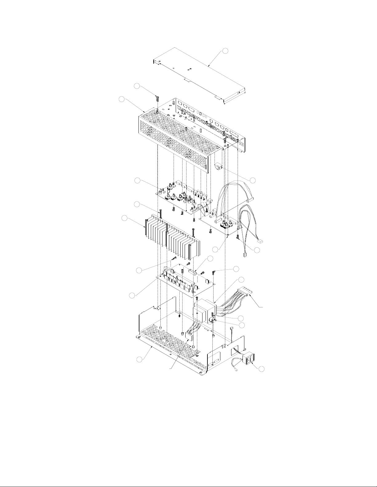
DISASSEMBLY/ASSEMBLY PROCEDURES
Main Assembly Procedures
Note: Certain parts will be referred to in
these procedures. The numbers in parentheses represent individual parts called out
in Figure 1. The callout numbers correspond to those on the part lists.
1. Chassis Cover/Top Cover Removal
1.1 Place the amplifier flat on the work-
bench with the Bose
corner.
1.2 Detach the chassis cover (1) by holding
both corners and pulling upward. Once the
cover is loosened, slide the bottom tabs out
and away from the unit.
1.3 Use a phillips-head screwdriver to
remove two silver screws (2) securing the
chassis top cover (3).
®
logo in the upper-left
2.2 Align the screw holes of the top cover
with the screw mounts located on the base.
Also align the four metal tabs on the base
with the tab slots on the cover. There are
also six metal tabs located on the bottom
edges of the cover that must be aligned
when the cover is finally seated.
2.3 Slide the cover down over the base
until the screw holes are aligned and all tab
slots are locked into place.
2.4 Secure the chassis top cover (3) by
tightening two silver screws (2) with a
phillips-head screwdriver.
2.5 Position the three bottom tabs on the
chassis cover into the slots located in the
chassis base. Press the chassis cover
down over the chasis-top cover to secure it.
3. Amplifier PCB Removal (Chassis Base)
1.4 Gently lift the right side of the chassis
top cover up at a 45° angle and pull to the
right and up. This is done to clear the left
screw mount away from the Amp PCB (8)
when the cover is lifted off.
IMPORTANT: Be careful not to pull the
three cables connected to the Amp PCB (8)
assembly. They must be disconnected
before final removal of the chassis-top
cover.
2. Chassis Cover/Top Cover Replacement
2.1 Place the chassis-top cover (3) over the
chassis base (4). Align the cover so that
the left-side screw mount of the chassis
base will slide between the IO1 PCB (8)
and the inside surface of the chassis-top
cover. Otherwise there will be difficulty
securing the cover.
3.1 Remove the Chassis Cover/ Top Cover
(Procedure 1) .
3.2 Separate the chassis-top cover from
the base by disconnecting both two-pin
cables from the Amp PCB's (8) P3A and
P3B connectors. Disconnect the eight-pin
cable from the Amp PCB's P2A connector.
3.3 Disconnect the following cables:
• Disconnect the transformer's five-pin
primary cable from the Amp PCB's P7
connector.
• Disconnect the transformer's five-pin
primary cable from the Amp PCB's P4
connector.
• Disconnect the main power two-pin
primary cable from the Amp PCB's P4
connector.
IMPORTANT: Be sure to notice the orientation of the transformer's five-pin primary
cable. Pin 1 is keyed to pin 1 of Amp PCB
connector P6 (or P7 depending upon the
unit's applicable voltage rating).
11
Page 12
CHASSIS COVER
1
2
CHASSIS
TOP COVER
COUPLER
BAR
3
IO1 PCB
7
8
6
IO2 PCB
8
8
AMP ASSY
5
9
P3B
P2
P5
P3A
5
10
12
5
CONNECT
TO P3B
BLU./GRY.
CONNECT
TO P3A
RED/BLK.
PRIMARY
5
2X
11
CONNECT
TO P5
CHASSIS
BASE
4
SECONDARY
13
Figure 1. Main Disassembly/Assembly Exploded View
12
Page 13

3.4 Remove two black screws (5) from the
Amp PCB (8) and three black screws (6)
from the Heatsink (7).
3.5 Remove the Heatsink/Amplifier PCB
Subassembly from the chassis base.
3.6 Place the subassembly on the workbench with the heatsink (7) fins down.
3.7 Remove three black decoupler bar
screws (5) that connect the heatsink to the
Amplifier PCB.
3.8 Remove the Amplifier PCB (8) from the
heatsink.
4. Amplifier PCB Replacement (Chassis
Base)
IMPORTANT: Thermal grease should be
applied to the heatsink before seating the
PCB.
4.4 Connect the following cables:
• Connect the main power's two-pin cable
to the Amp PCB's P5 connector.
• Connect the tranformer's secondary fivepin cable to the Amp PCB's P4 connector.
• Connect the transformer's primary five-pin
cable to the Amp PCB's P7 connector.
IMPORTANT: Pin 1 of the transformer's
five-pin primary cable is keyed to pin 1 of
Amp PCB connector P6 (or P7 depending
upon the unit's applicable voltage rating).
4.5 Install the Chassis Cover/Top Cover
(Procedure 2).
5. Transformer Removal
5.1 Remove the Chassis Cover/Top Cover
(Procedure 1).
5.2 Disconnect the following cables from
the transformer:
4.1 Place the Amplifier PCB (8) onto the
heatsink (7). Align the coupler bar (9) screw
holes with the screw holes of the heatsink.
The PCB should be component side up
with the power devices resting on the inner
side of the heatsink.
4.2 Secure the coupler bar and Amplifier
PCB to the heatsink by tightening three
black screws (5).
IMPORTANT: Make sure that the coupler
bar does not make contact with the metal
tab of transistor Q305.
4.3 Place the Heatsink/Amplifier PCB
subassembly solderside down into the
chassis base. Secure the upper-left hand
corner of PCB onto the standoff snap.
Secure the subassembly to the chassis
base by tightening two black screws (5) on
the Amp PCB and three black screws (6)
on the heatsink.
• Disconnect the transformer's five-pin
primary cable from the Amp PCB's P7
connector.
• Disconnect the transformer's five-pin
primary cable from the Amp PCB's P4
connector.
5.3 Remove transformer cables from cable
clamps (12) and lift the transformer from
the chassis base (4).
6. Transformer Replacement
6.1 Place the transformer (10) into the
recess of the chassis base and align it with
the chassis base mounting holes. Make
sure that the primary side is facing the IEC
Connector Assembly
(13).
6.2 Place the two transformer clips (11)
over the transformer's mounting tabs.
Secure the transformer to the chassis base
by tightening the two black screws (5).
13
Page 14

6.3 Connect the following cables:
• Connect the transformer's five-pin secondary cable to the Amp PCB's P4 connector.
• Connect the transformer's five-pin primary cable to the Amp PCB's P7 connector.
IMPORTANT: Pin 1 of the transformer's
five-pin primary cable is keyed to pin 1 of
Amp PCB connector P6 (or P7 depending
upon the unit's applicable voltage rating).
6.4 Install the Chassis Cover/Top Cover
(Procedure 2).
7. IO1 & IO2 PCB Removal (Chassis Top)
7.1 Remove the Chassis Cover/Top Cover
(Procedure 1).
8. IO1 & IO2 PCB Replacement (Chassis
Top)
8.1 Connect the 12-pin cable to connector
P1A on the larger board.
8.2 Carefully align both board's connectors
into the chassis top cover and snap them
onto the chassis standoffs.
8.3 Secure the two-pin and the eightpin cables into the cable clamps (12).
8.4 Replace six black screws (5) and
tighten to secure both boards.
8.5 Install the Chassis Cover/Top Cover
(Procedure 2).
7.2 Remove six black screws (5) from both
Amplifier IO PCB's (8). Remove the IO2
PCB board first. Grasp it by the top corners, lift up and off the chassis-top's standoffs. (Note: The IO boards are connected
by a 12-pin cable. Do not attempt to separate until both are removed).
7.3 Remove both two-pin and eight-pin
cables from the cable clamp (12) from the
inside of the chassis-top cover.
7.4 Grasp the IO1 PCB board by its top
corners, lift up and off the chassis-top's
standoffs. Position the board at a 45° angle
and carefully pull it back so that the I/O
connectors clear the top cover.
7.5 To separate boards, disconnect the 12pin cable from connector P1A on the larger
board.
14
Page 15

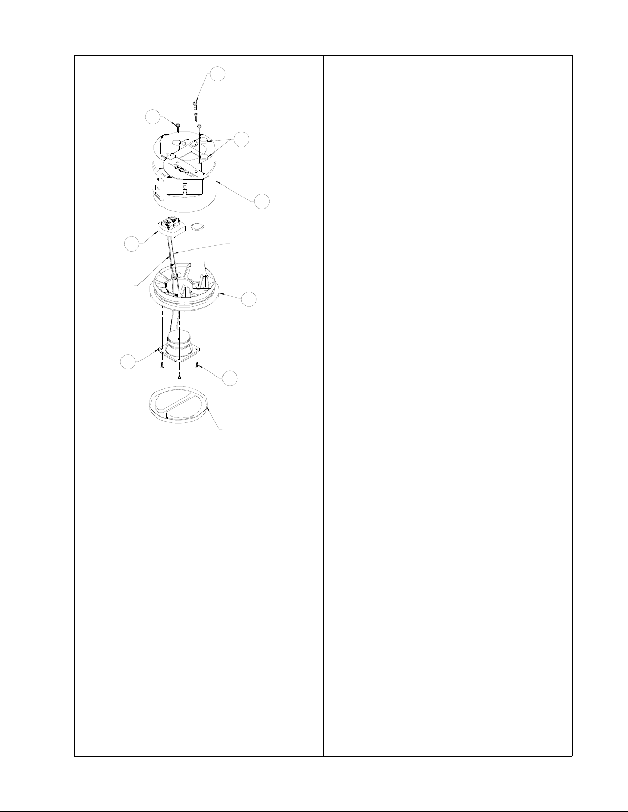
Flush-Mount Loudspeaker Procedures
1. Flush-mount Loudspeaker
NOTES: Certain parts will be referred to in
these procedures. The numbers in parentheses correspond to the individual parts
called out in Figure 2.
C. Use Procedure 1.2 to return the grille to
the enclosure.
1.5 Terminal Cup Removal
A. Use a phillips-head screwdriver to
remove one screw (7) from the junction-box
cover.
1.1 Grille Removal
To remove the grille (Not Shown) take a
scribe or a small flat-head screwdriver to
grasp an edge of the grille. Gently lift the
grille out from the enclosure (2).
1.2 Grille Installation
Push the grille into the enclosure (2) until it
is flush with the rim of the enclosure.
Orientation of the logo is not necessary.
1.3 Driver Removal
A. Use Procedure 1.1 to remove the grille
from the enclosure (2).
B. Use a phillips-head screwdriver to
remove four screws (3) securing the driver
(4) to the enclosure's baffle (6). Carefully lift
the driver from the enclosure and cut the
wires as close to the terminals as possible.
1.4 Driver Replacement
A. Strip the terminal wires from the terminal
cup (5) and connect them to the replacement driver (4). Connect the red wire to the
+ positive terminal and the black wire to the
- negative.
B. Swivel the junction-box cover out to
expose the terminal cup (5) in the recess of
the speaker enclosure (2).
C. Use a phillips-head screwdriver to
remove three screws (3) that secure the
terminal cup to the speaker enclosure.
D. Use Procedure 1.3 to remove the driver
(4) from the speaker enclosure (2).
E. Disconnect the terminal wires from the
driver and remove the faulty terminal cup.
1.6 Terminal Cup Replacement
A. Use Procedure 1.4 to connect the
replacement terminal cup (5) to the driver
(4).
B. Place the enclosure (2) on its side. Fit
the terminal cup into the slot at the back of
the enclosure. See Figure 2 for the proper
orientation of the terminal.
C. While holding the terminal from the
inside of the enclosure, tighten three
screws (3) with a phillips-head screwdriver.
D. Use Procedure 1.4 to secure the driver
(4) to the enclosure.
B. Align the driver so their four screw holes
align with the screw holes of the
enclosure's baffle (6). Secure the driver to
the enclosure (2) by tightening four screws
(3) with a phillips-head screwdriver.
E. Use Procedure 1.2 to secure the grille
to the enclosure.
15
Page 16
Junction-Box
Cover
7
Surface-Mount Loudspeaker Procedures
1. Surface-Mount Loudspeaker
3
NOTE: The Surface-mount Loudspeaker
8
has only two removable and replaceable
parts, the grille and the grille's scrim cloth.
Refer to the Surface-mount Assembly Part
List for the grille and scrim cloth's order
2
numbers.
1.1 Grille Removal
5
Red
4
Black
The Baffle is
6
Adhered to
Enclosure
3
Item 1 on the
Packaging Part List
Figure 2. Flush-Mount Loudspeaker
Exploded View
Grasp one edge of the grille with a small
scribe and gently pull the grille from the
enclosure. The grille's scrim cloth is behind
the grille.
1.2 Grille Replacement
1. Place the scrim cloth inside the grille.
2. Place the grille over the twiddler section
of the enclosure (Refer to Figure 3 for the
correct orientation). Press the grille until it
snaps into place.
16
Page 17
Grille
Figure 3. Surface-mount Loudspeaker
17
Page 18
TEST PROCEDURES
Main Assembly Test Procedures
Test Set-Up Parameters
Switches
All switches are referenced by their block
diagram location on the top of the unit. Set
them according to the table below.
Block
No.
10 Line Output Mode center(Music
Switch Description Setting(s)
1 Page Source Gain left (0dB)
2 Optivoice Compressor left(off)
5 Page Enables Left and
Right
7 Music Compressors A
and B
9 Music Input Mode rear(stereo)
right(on)
forward(off)
+Page)
Input Connections
Page Input
Connect the positive (+) side of an oscilla-
tor to the positive input terminal. Connect
the negative (-) side to the negative (-) and
common input terminals. Do this using
quick connectors (P/N180094) supplied
with the unit.
Music RCA Inputs A, B (Left and Right)
Connect the positive (+) side of an oscilla-
tor to the positive input terminal on the RCA
jack. Connect the negative (-) side to the
negative (-) and RCA jack ground sleeve.
Output Connections
Page and Line Outputs (Left and Right)
Potentiometers
All potentiometers are referenced by
their block diagram location on the top of
the unit. Set them according to the table
below.
Block
No.
1 Page Source Gain
3 Page Trigger
4 Page Mix Trim cw(max)
6 Music A and B Source
12 Treble and Bass Trim center(flat)
13 Volume Trim Right cw(max
Pot. Description Setting(s)
ccw(0dB)
Trim
cw(max)
Level
cw(max
Trim
gain)
gain)
Connect the positive (+) side of the test
equipment to the positive (+) output terminals. Connect the negative (-) side to the
negative (-) output terminals. Do this using
quick connectors (P/N180094) supplied
with the unit.
Speaker Output (Left and Right)
Use the same output connections as above
with a 2Ω/50Watt resistor as a load.
All test equipment should be isolated
from ground (floated).
18
Page 19

1. Page Input To Page Output Gain
6. Noise
1.1 Apply a 5 Vrms, 1KHz signal to the
Page Input.
1.2 Measure the Page Output. Should be
4.22 Vrms (+ .78 Vrms/ - .67 Vrms).
2. Page Input To Line Outputs Gain
2.1 Apply a 5 Vrms, 1KHz signal to the
Page Input.
2.2 Measure the left and right Line Output.
Should be 4.22 Vrms (+1.09 Vrms/ -.87
Vrms).
3. Music Input A to Line Outputs Gain
3.1 Apply a 500mV rms, 1KHz signal to the
Music A left and right input.
3.2 Measure the left and right Line outputs.
Should be 4.47 Vrms (+.84 Vrms/ - .71
Vrms).
Note: Repeat this test for Music Input B.
To select Music Input B, short the remote
select input.
4. Music Input A to Speaker Outputs Gain
6.1 Set the volume control to Max.
6.2 With the source off, measure the left
and right Speaker output. Should be
mVrms.
7. Full Power Distortion
7.1 Apply a 130 mVrms, 800 Hz signal to
the left input.
7.2 Measure the distortion at the left
Speaker output. Should be
7.3 Change the frequency to 95 Hz and
adjust the applied signal to get 5.66 Vrms at
the left Speaker output.
7.4 Measure the distortion at the left
Speaker output. Should be
Note: Repeat this procedure for the right
channel.
8. Separation
8.1 Apply a 100 mVrms, 800Hz to the right
Music A Input. Terminate the left Music A
Input with a 50
Ω resistor.
≤ 1% THD.
≤ 2 %.
≤ 5.6
4.1 Apply a 10 mVrms, 2KHz signal to the
left and right Music A input.
4.2 Measure the Speaker output. Should be
290 mVrms (+54mVrms/ - 46mVrms).
5. Frequency Response
5.1 Apply a 10 mVrms, 2KHz signal to the
left and right Music A Input.
5.2 Reference a dB meter to the Speaker
output and set level to 0 dBr.
5.3 Change the signal to 12.5 KHz.
5.4 Measure the left and right Speaker
output. Should be 5.1 dBr (
± 2.0 dB).
8.2 Measure the left Speaker output.
Should be
Note: Repeat this procedure for the right
channel.
19
≤ 10 mV.
Page 20

Loudspeaker Test Procedures
NOTE: These procedures apply to both Flush-mount and surface-mount loudspeakers. The surface-
mount loudspeaker is not repairable. If this loudspeaker fails the following tests contact your Bose® Field
Service Representative.
1. Rub and Tick Test
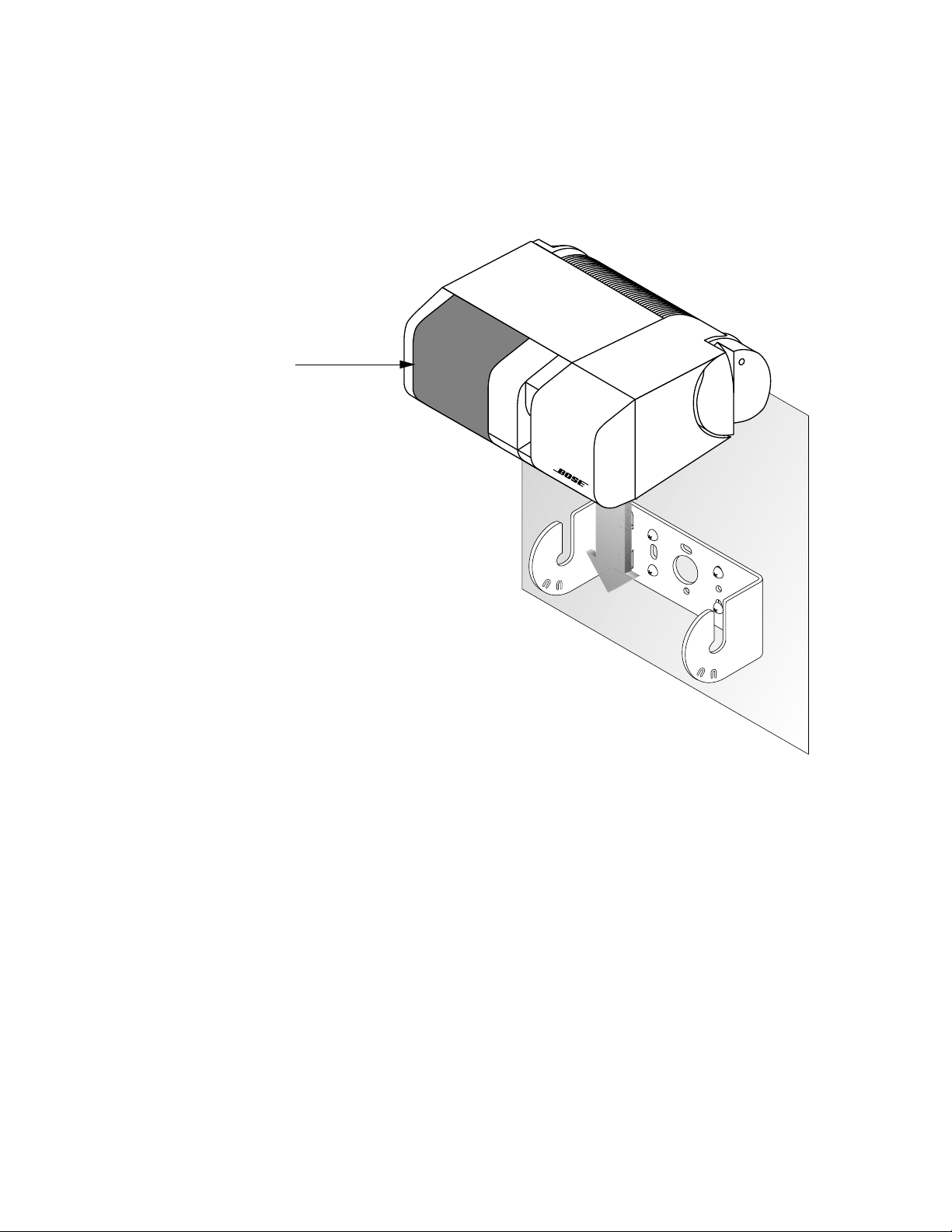
Apply a signal of 6.0 Vrms at 80 Hz to the input terminals of the loudspeaker. See Figure 1. No
extraneous noises such as rubbing or ticking should be heard. Replace any driver that has a rubbing or
ticking noise.
NOTE: There is a normal suspension noise. To distinguish between a rub or tick and suspension noise,
displace the cone slightly with your finger. If the rubbing can be made to go away or get worse, then it is a
rub or tick and the driver should be replaced. If the noise stays the same, it is a suspension noise and the
driver is fine. Suspension noise will not be heard with program material.
2. Air Leak Test
Apply a signal of 6.0 Vrms ± 1V at 80 Hz to the speaker input terminals. See Figure 1. For at least 5
seconds, listen for air leaks around the driver, speaker terminals, and along all cabinet joints. Repair air
leaks as required.
3. Sweep Test
Sweep the oscillator from 50 Hz to 5 kHz at 6Vrms. There should not be any loud extraneous sounds. If
there are any loud buzzes or distortion, replace the driver. The whooshing noise from the port at around
80 Hz is acceptable.
NOTE: There should not be any buzzes or rattles from the internal connecting wires or components.
Redress any wire or component that buzzes.
Input Terminals
Figure 1. Input Terminals
4. Phase Test
NOTE: Supply voltage should only be momentarily applied to the speaker input terminals to avoid
possible damage to the speaker.
Apply a 6 Vdc ± 1 Vdc signal to the speaker input terminals (see Figure 1). The driver should move
outward.
20
Page 21

PART LISTS AND EXPLODED VIEWS
The following section contains part lists and exploded views for the FreeSpace®6 business
music system. The part lists are broken down as follows:
• Main Assembly Part List and Main Assembly Exploded View.
• Remote Assembly Part List and Remote Assembly Exploded View
• Main Assembly Packaging Part List and Main Assembly Packaging Exploded View.
• Flush-mount Loudspeaker Assembly Part List and Exploded View.
• Flush-mount Loudspeaker Assembly Packaging Part List and Packaging Illustration.
• Surface-mount Loudspeaker Assembly Part List and Illustration.
• Surface-mount Loudspeaker Assembly Packaging Part List and Packaging View.
• Electrical Part Lists : These lists contain all electrical and mechanical parts located
on the PCB assembly 177300, Revisions 0 and 1.
PCB layouts and schematics are located in the back of the service manual.
21
Page 22

Main Assembly Part List (Figure 4)
Item
Number
Description Part Number Qty
Per
See
Note
Assy
1
Chassis,Cover,FreeSpace®6
2 Screw,Mach,8-32,Pan,Xrec/Slot 172715-08 2
3 Chassis,Top Cover,FreeSpace 6 177286 1
4 Chassis,Base,FreeSpace 6 177285 1 4
5 Screw,#8-32x.25,Pan,Xrec 179096-04 13
6 Screw,#8-32x2.75,Pan,Xrec 179096-44 3
7 Heatsink,FreeSpace 6 177283 1 4
8 Pcb Assy,FreeSpace 6,Amp,S/f 181692 1 1,3
9 Coupler Bar,FreeSpace 6 177284 1
10 Transformer,120/240V,FreeSpace 6 177278 1 2
!
Transformer,100V,FreeSpace 6 178892
177287 1
11 Clip,Transformer 179108 2
12 Clip,Cable,Dbl Face Adh,.76" 131062 3
13 Conn Assy,IEC Receptical 179064 1
14 Nut,Hex,8-32,keps 100413-2 1
Notes:
1. The individual parts located on the PCB's are listed in the Electrical Part List.
!
2. This part is critical for safety purposes. Failure to use a substitute replacement
with the same safety characteristics as the recommended replacement part might create
shock, fire and/or other hazards.
3. The PCB Assembly is divided into three parts: the Amplifier PCB, IO1 PCB, and IO2
PCB. The PCB locations are identified on the FreeSpace 6 Exploded View. This
information is provided for reference only.
4. This part is not normally available from Customer Service. Approval from the Field
Service Manager is required before ordering.
22
Page 23

CHASSIS
TOP COVER
3
IO1 PCB
7
1
CHASSIS COVER
2
LOCATE WITHIN
BOX EMBOSSED
ON CHASSIS
12
1
1
1
1
8
6
12
C43
LOCATE WITHIN
12
BOX EMBOSSED
ON CHASSIS
14
COUPLER
BAR
CHASSIS
BASE
9
5
4
IO2 PCB
SECONDARY
P3B
8
AMP ASSY
8
P2
P3A
P5
CONNECT
TO P5
5
10
5
11
5
CONNECT
TO P3B
2X
PRIMARY
13
Figure 4. Main Assembly Exploded View
TOP VIEW
23
Page 24

Remote Assembly Part List
Item
Number
Description Part Number Qty
Per
See
Note
Assy
1 PCB Assy,FreeSpace 6,AMP,S/F 181692 1
2 Cover,Remote,FreeSpace 6,Europe 178101 1
Cover,Remote,FreeSpace 6,Japan 178102 1
Cover,Remote,FreeSpace 6,Aus,Am/Can 178103 1
3 Knob,Remote,FreeSpace 6 178104 1
4 Screw,OVLHD,6-32x1.00,Am/Can 178115-16 2
Screw,OVLHD,M3.5x25mm,Aus,Europe 178116-25 2
Screw,OVLHD,M4x25mm,Japan 178117-25 2
5 Screw,TAPP,6-13x.5,PAN,XREC 173555-08 2
6 Cable Tie 135540 2
7 Bag,Poly,6x10x5 mil 147794 1
4
3
2
1
6 2 PLCS.
BLACK
YELLOW
7
5
Figure 5 Remote Assembly Exploded View
24
Page 25

Main Assembly Packaging Part List (Figure 5)
Item
Number
Description Part Number Qt y
Per
See
Note
Assy
1 Packing, Endcap, EPS, Left 177949 1
2 Polybag, 12"x8"x24" 143076 1
3 Packing, Endcap, EPS, Right 177305 1
4 Rem,RVC Walplt,Frspc 6,US/CAN 178111 1
Rem,RVC Walplt,Frspc 6,Eur 178113
Rem,RVC Walplt,Frspc 6,Japan 178112
Rem,RVC Walplt,Frspc 6,Australia 181735
5 Packing, Crease Sheet 177950 1
6 Line Cord,120V,Detachable, US/CAN 173350 1 1
!
Line Cord,230V,Detachable,UK 173351
Line Cord,230V,Detachable,Europe 173352
Line Cord,240V,Detachable,Australia 173354
Line, Cord,100V,Detachable,Japan 181690
7 Carton, RSC 177948 1
8 Lit kit Assy,FS6,F/S,Japan 181704-1 1
Lit kit Assy,FS6,F/S, Australian, Eur,UK,
181704-2
US/Can
9 Connector Kit, Assy 180094 1
Note:
!
1. This part is critical for safety purposes. Failure to use a substitute replacement
with the same safety characteristics as the recommended replacement part might create
shock, fire and/or other hazards.
25
Page 26

8
1
2
3
9
4
5
6
7
Figure 6. Main Assembly Packaging Exploded View
26
Page 27

Flush-mount Assembly Part List
Item
Description Part Number Qty See
Number
1 Grille Assy. 1
2 Enclosure Assy, Back Can, 102-F6 ----------- 1 *
3 Screw, Hilo, 8, Pan, Xrec 172721-10 7
4 Twiddler, 2.25" 149167 1
5 Cup, Terminal 176459 1
6 Baffle, 75 Cu In, White ----------- 1 *
7 Screw, Mach, 8-32, Pan,Xrec/Slot 172715-08 1
8 Foot, Clear, .312x.085, Bulk 178321-99 2
*This part was listed and illustrated for reference purposes only.
7
Note
Junction-Box
Cover
5
Red
4
3
8
2
Black
The Baffle is
6
Adhered to
Enclosure
3
Item 1 on the
Packaging Part List
Figure 7. Flush-mount Exploded View
27
Page 28

Flush-mount Packaging Part List
Item
Description Part Number Qty See
Number
1 Shield, Paint 180092 1
2 Grille Assy, 4pk, Wht 178133-2 1
3 Pan Mounting Assy, 4 Pk 178135 1
4 Spring Assy, 8 Pack, Freespace 6 178132 1
5 Carton, RSC 177752 1
6 Packing, Insert 177744 1
7 Packing, Crease Sheet, 18x21 177749 1
8 Packing, Crease Sheet, 16.07x5.75 177747 1
9 Packing, Crease Sheet, 20.75x17.0 177750 1
10 Bushing, Short,.75" 146046 1
11 Bag,Poly, 14.38x9.87x2 Mil 103351 1
12 Packing, Sheet, 8.75x8.75x.03 180023 1
Note
7
10
9
8
4
2
12
3
6
5
Figure 8. Flush-mount Loudspeaker Packaging Illustration
28
Page 29

Surface-mount Assembly Part List
Item
Description Part Number Qty See
Number
1 Knob, White 178149-02 1
Knob, Gray 178149-01 1
2 Grille, Speaker, Computer Gray 177146-01 1
Grille,Speaker, Arctic White 177146-02 1
3 Cloth, Scrim, Grille 181192 1*
*Part not illustrated
Note
23
1
Figure 9. Surface-mount Loudspeaker Illustration
29
Page 30

Surface-Mount Packaging Part List
Item
Description Part Number Qty
Number
1 Bracket, Wall, White 178146-02 4
Bracket, Wall, Gray 178146-01 4
2 Knob And Pkg Assy, Arctic White 181736-02 1
Knob And Pkg Assy, Gray 181736-01 1
3 Carton, 4 Pack 181535 1
4 Packing, End Cap, 181537 8
5 Packing, Crease Sht, 46.5x8.5 181536 1
6 Bag, Poly, 14.38x9.87x2 Mil 103351 4
2
5
Per
Pack
See
Note
1
6
4
3
Figure 10. Surface-mount Loudspeaker Packaging
30
Page 31

FreeSpace®6 Electrical Part List
PCB P/N 177300, Revision 0
Resistors
Reference
Description Part Number Reference
Designator
R1 Pot,Rotary,50kΩ,
10%,Dual
R2,3,5 Pot,Rotary,10kΩ,
10%,Single
R6-9 Pot,Rotary,10kΩ,
10%,dual
R10,11,27,3639,44,45,47,50,52,
53,55,56,61,63,64,
65,70-72,75,85,89,
96,99,101,107,110,
116,128,129,130,
135,152,202,204,
206,212,213,218,
219,221,222,240,
256,265,275,315,
319,321,322,336,
339,345, 378,379
R12,203,214,362 402Ω,1%,1/10W,
R13,18,59,76,87,94,
127, 137,291,331,
335, 355
R14-17,21,34,35,62,
66, 79,88,95,98,103,
106,109,112,136,
287,320
R19,20,86 1.54KΩ,1%,1/10W,
R22,23,311 5.62KΩ,1%,1/10W,
R24,25,28,29,31,
113,123,124,307,
310, 377
R26,253,255,267,
269,312
R32,58,74,151,257,
258,264,266,305
R33,90,92 1.2KΩ,2%,1/4W,
R40,117,200,216,
350,376
R41,208,306 301KΩ,1%,1/10W,
R42 26.7KΩ,1%,1/10W,
R43,121,143,201,
210,217,236,
10.0KΩ,1%,1/10W,
0805
0805
30.1KΩ,1%,1/10W,
0805
1.00KΩ,1%,1/10W,
0805
0805
0805
20.0KΩ,1%,1/10W,
0805
7.50KΩ,1%,1/10W,
0805
1MΩ,5%,1/10W,
0805
52mm,CF
100Ω,1%,1/10W,
0805
0805
0805
301Ω,1%,1/10W,
0805
177289-503
177290-103
177289-103
133625-1002
133625-4020
133625-3012
133625-1001
133625-1541
133625-5621
133625-2002
133625-7501
133626-1055
121243-1211222
133625-1000
133625-3013
133625-2672
133625-3010
31
Page 32

FreeSpace®6 Electrical Part List
PCB P/N 177300, Revision 0
Resistors (Continued)
Reference
Description Part Number Reference
Designator
R46,54,73,209 56.2KΩ,1%,1/10W,
0805
R51,119,120,125,12
6, 138-141,325,346
R57,91,97,102,104,
111,133,157,160,
207,224,241,277,
279,304,317,358
R60,78 68.1KΩ,1%,1/10W,
R67,83,237,301,333
353
R68 15.0KΩ,1%,1/10W,
R69 45.3KΩ,1%,1/10W,
R77,84 127KΩ,1%,1/10W,
R80 26.1KΩ,1%,1/10W,
R81 1.82KΩ,1%,1/10W,
R82,131,154 17.8KΩ,1%,1/10W,
R91,205,215,278,
326,327,347,349
R93,118,318 2.43KΩ,1%,1/10W,
R100,108 2.55KΩ,1%,1/10W,
R105,316,368, 370 47.5KΩ,1%,1/10W,
R114,357 200KΩ,1%,1/10W,
R115,134 73.2KΩ,1%,1/10W,
R122,142 4.75Ω,1%,1/10W,
R132,145,148,161,
232,242,260,262,
276,290,292,356,
374,380,381
R144,323,338,343,
363
R146,147,149,150 255Ω,1%,1/10W,
61.9KΩ,1%,1/10W,
0805
100KΩ,1%,1/10W,
0805
0805
4.12KΩ,1%,1/10W,
0805
0805
0805
0805
0805
0805
0805
15.0KΩ,1%,1/10W,
0805
0805
0805
0805
0805
0805
0805
Jumper,Chip,0805
2.00KΩ,1%,1/10W,
0805
0805
133625-5622
133625-6192
133625-1003
133625-6812
133625-4121
133625-1502
133625-4532
133625-1273
133625-2612
133625-1821
133625-1782
133625-1503
133625-2431
133625-2551
133625-4752
133625-2003
133625-7322
133625-4R75
133627
133625-2001
133625-2550
32
Page 33

FreeSpace®6 Electrical Part List
PCB P/N 177300, Revision 0
Resistors (Continued)
Reference
Description Part Number Reference
Designator
R153 27.4KΩ,1%,1/10W,
0805
R155158,239 5.11KΩ,1%,1/10W,
0805
R156,159 Pot,Rotary,10KΩ,
10%, 1/2W,Trim
R211,280,340 88.7KΩ,1%,1/10W,
0805
R220,223 11.0KΩ,1%,1/10W,
0805
R238,308,309,313,
314
R254,259,268,274 18.2KΩ,1%,1/10W,
R270-273 57.6KΩ,1%,1/10W,
R300 25.5KΩ,1%,1/10W,
R302 6.49KΩ,1%,1/10W,
R303,324,344 14.0KΩ,1%,1/10W,
R324,337,359 7.15KΩ,1%,1/10W,
R328,352 110KΩ,1%,1/10W,
R329,342 9.09KΩ,1%,1/10W,
R330,354 23.7KΩ,1%,1/10W,
R332,334,348,351 4.99KΩ,1%,1/10W,
R341,375 38.3KΩ,1%,1/10W,
R364 2.74KΩ,1%,1/10W,
R366,367,369,372 RES,CF,1/4W,5%,1
R371 Jumper,22AWG,
R373 196Ω,1%,1/10W,
R500 Pot,Rotary,10kΩ,
4.75KΩ,1%,1/10W,
0805
0805
0805
0805
0805
0805
0805
0805
0805
0805
0805
0805
0805
0 OHM
Non-Insul,10.0mm
0805
10%
133625-2742
133625-5111
170042-103
133625-8872
133625-1102
133625-4751
133625-1822
133625-10R0
133625-2552
133625-6491
133625-1402
133625-7151
133625-1103
133625-9091
133625-2372
133625-4991
133625-3832
133625-2741
121243-1211005
148242-100
133625-1960
177299-103
33
Page 34

FreeSpace®6 Electrical Part List
PCB P/N 177300, Revision 0
Capacitors
Reference
Description Part Number Reference
Designator
C1,2,29,123,200,
205
C3,7,23,24,25,35,
47,50,51,63,89,93,
100,103,116,117,
118,119, 120
C4,5,36,38,54,86,
90,102,105,202,217,
227,237,301,304,
309,335,348
C6,14,19,39,106,
107,112,113,
114,115,121,122
C8,11,15,18,20,27,
32,46,53,57,62,65,
76, 77,80,81,88,92,
94, 95,96,101,109,
110, 153,201,204,
206, 208,216,218,
220, 222,223,226,
238, 300,307,308,
310, 311,321,324,
501, 512
C9,43,55,79,98,207,
219,312,322
C10,41,59,224,239 10pF,5%,50V,0805,
C12,17,108,111,
242,243,244,245,
339, 340,353,354,
357,361,362
C13,314,315,329,
330
C16,320,331,355,
356, 359,360
C21,26,49,52,70,74 680pF,5%,50V,
C22,48,68,69,71,75,
84
C28 47uF,20%,16V,105,
C30,33,34,37,40,56,
58,61,66,67,83,85
C31,72,73,78,82,
333,334,349,352
C42,303 15uF,5%,50V,85,
.01uF,10%,50V,
X7R,0805
47pF,5%,50V,0805,
COG
10uF,20%,35V,85,
EL
100pF,5%,50V,
0805,COG
.022uF,10%,50V,
X7R,0805
1.0uF,20%,50V,105,
EL
COG
.10uF,80%,25V,
Y5V,0805
18uF,5%,50V,85,
BOX
1000pF,5%,50V,
0805,COG
0805,COG
4.7uF,20%,35V,105,
EL
EL
2.2uF,20%,50V,105,
EL
.1uF,5%,50V,85,
BOX
BOX
133623-103
133622-470
149948-100V
133622-101
133623-223
137126-1R0
133622-100
133624
137127-184
133622-102
133622-681
137126-4R7
137126-470
137126-2R2
137127-104
137127-154
34
Page 35

FreeSpace®6 Electrical Part List
PCB P/N 177300, Revision 0
Capacitors (Continued)
Reference
Description Part Number Reference
Designator
C44 220uF,20%,25V,85,
EL
C45,60 100uF,20%,25V,85,
EL
C64,319,327,337,
350, 351
C87 .47uF,5%,50V,85,
C104,203,341,342 22uF,20%,25V,85,
C225,240,248-250 390pF,5%,50V,0805
C228,241 .0012uF,5%,100V,
C229,230,246,247 .047uF,5%,63V,85,
C302 .068uF,5%,63V,85,
C306 1800pF,10%,50V,
C313,317,325,326 .0015uF,5%,100V,
C336,345 2200uf,20% ,50v,
C344,346,347 3300uf,20%,35v,
C363,364 1000pf,20%,250vac,
!
.22uF,5%,50V,85,
BOX
BOX
EL
,COG
85, BOX,
BOX
BOX
X7R,0805
85,BOX
105,EL
105,EL
Y-type,
149948-221E
149948-101E
137127-224
137127-474
149948-220E
133622-391
137127-122
137127-473
137127-683
133623-182
137127-152
144000-222H
144000-332V
170183
Note:
!
1. This part is critical for safety purposes. Failure to use a substitute replacement
with the same safety characteristics as the recommended replacement part might create
shock, fire, and/or other hazards.
35
Page 36

FreeSpace®6 Electrical Part List
PCB P/N 177300, Revision 0
Diodes
Reference
Description Part Number Reference
Designator
D1,3,4,6 LED,2.5v,10ma
Green,Vertical
D2,5 LED,2.5v,10ma,
Grn/Red,Vertical
D10,11,13-
Dual,SOT-23,BAV99 147239
17,22,24,107,201,
204,300
D12,20,21,200,302,
309,310
Switching,75V,
300mA
D18,19,23,202,203 Zener,18V,1W,5%,
1N4746
D25,27,29,301 Dual,SOT-23,BAV70 147249
*D305 Rectifier,Bridge,
!
100v,1.0a
*D306 Rectifier,Bridge,
!
1 00v,6a
D307 Zener,16V,1W,5%,
1N4745
Transistors
177280
177281
121501
116995-4746A
143952 *See Note 1
170214 *See Note 1
116995-4745A
Reference
Description Part Number Reference
Designator
Q1,2,202,300,304 BPLR,N,40V,200mA
,SOT23
Q3-7 BPLR,N,SOT23,2S
D2114K
Q200 BPLR,P,60V,200mA,
TO-92
Q201 BPLR,N,30V,500mA
,TO-92
Q203,301,302 BPLR,P,40V,200mA,
SOT23
Q305 DARL,NPN, Tip140 177310
Note:
!
1. This part is critical for safety purposes. Failure to use the recommended
replacement part may create shock, fire and/or other hazards.
146819
177294
119168
173476
148596
36
Page 37

FreeSpace®6 Electrical Part List
PCB P/N 177300, Revision 0
Integrated Circuits
Reference
Description Part Number Reference
Designator
U1-4,10,15,200,
202-205,301
U11,12 Switch,Active,
U201 Op-Amp,Dual,
U302 Op-Amp,Single,
U5,7 Compandor,
U6,13,14,300,303 OpAmp,Quad,
U8 Multiplexer/
U9 Multiplexer,
U302 Op Amp,Sngl,DIPU304,307 Power Amp,Mult-11,
U305 Voltage
U306 Voltage
Op-Amp,Dual,
DIP-8,RC4559
SIP-8,BA3128N
DIP-16,CN3280
DIP-8,CA3080
NE572N
DIP-14,NJM2059
Demultiplexer,8CH,
DIP-16,4051
DIP-16,CD4052
8,CA3080
45W,TDA7396
Regulator,15V,Pos.,
TO-220
Regulator,15V,Neg.,
TO-220
108568
177292
133171
119834
178894
144008
177308
147243
119834
177279
143858
143806
37
Page 38

FreeSpace®6 Electrical Part List
PCB P/N 177300, Revision 0
Miscellaneous Components
Reference
Description Part Number Reference
Designator
*F1,2 Fuse,630ma
!
5x20mm
*F3,4 Fuse,Time
!
Lag,Auto,400mA
(Inv.)
*F5 Fuse,10.0A,
!
5x20mm,Slo Blo
*F6 Fuse,3.0A,250V,
!
.60x.19,Slo Blo
FC1A,2A,5A,F61A,
Fuseclip,5mm 178548
62A,65A,FC1B,C2B,
C5B, F61B,62B,65B
JP300 Jumper,22AWG,
Non-Insul. ,10.0mm
J1,2,9,10 Connector,Rt.Ang.,
3 pos,Blk
J11,8 Connector,Rt.Ang.,
2 pos,Blk
J12 Connector,Rt.Ang.
Beau
J3 Connector,Rt.Ang.,
5 pos,Blk
J4,5 Connector,RCA,
Dual,Female
K1 Relay,24 Vdc,4PDT 144017
P1 Harness,26
AWG,Freespace 6
P1A Connector,Header,
12 pos
P2 Harness,24
AWG,Freespace 6
P2A Connector,Header,
8 pos
P3 Harness,22
AWG,Freespace 6
P3A ,3B Connector,Header,
Inline,PCB Mnt.,2p
P4 Connector,Header,
Inline,PCB Mnt.,5p
P5 Connector,Header,
2 pos
P6 Connector,Header,
High Current 8mm
pitch
140346-0630 *See Note 1
177312-0400 *See Note 1
177311-10000 *See Note 1
135677-10 *See Note 1
148242-100
177291-03
177291-02
177291-08
177291-05
177295
177298-12
148591-12
177298-08
148591-08
177296
133220-02
133220-05
143963
178742-4
38
Page 39

FreeSpace®6 Electrical Part List
PCB P/N 177300, Revision 0
Miscellaneous Components
Reference
Description Part Number Reference
Designator
P7 Connector,Header,
178742-4
High Current 8mm
pitch
P9 Connector,Header,5
148591-05
pos
S1-6,S9 Switch,Slide,DPST,
176148
Vertical
S7 Switch,Slide,DPDT 176147
S10 Switch,DIP,SPST,
148777-1
4 pos.
SW500 Switch,SPST,
178108
Rocker
TP1-9,10,500, Connector,Header,
171621-0103
Test Jack,1
pos.,OR
VR300 Varistor,Met. Oxide,
!
170189
275V,75 joule
Note:
!
1. This part is critical for safety purposes. Failure to use a substitute replacement
with the same safety characteristics as the recommended replacement part might create
shock, fire and/or other hazards.
39
Page 40

FreeSpace®6 Electrical Part List
PCB P/N 177300, Revision 1
Resistors
Reference
Description Part Number Reference
Designator
R1 Pot,Rotary,50kΩ,
10%,Dual
R2,3,5 Pot,Rotary,10kΩ,
10%,Single
R6,7 Pot,Rotary,20kΩ,
10%,Dual
R8,9 Pot,Rotary,10kΩ,
10%,Dual
R10,11,27,36-39,
44,45,47-50,52,53,
55,56,61, 63-65,
70-72,75,85,89,96,
99,101,107,110,116,
128-130,135,152,
202,204,206,212,
213,218,219,221,
222,232,240,242,
256,265,275,315,
319,321,322,336,
339,345,378,379
R12,203,214,362 402Ω,1%,1/10W,
R13,18,59,76,87,94
127,137,291,331,
355
R14-17,21,34,35,62,
66,79,88,95,98103,
106,109,112,136,
229,247,287,320
R19,20,86,226,231,
249,252
R22,23 5.62KΩ,1%,1/10W,
R24,25,28,29,31,
113,123,124,155,
158,307,310,377
R26 7.50KΩ,1%,1/10W,
R32,58,74,151,257,
258,264,266,305
R33,90,92 1.2KΩ,2%,1/4W,
R40,117,200,216,
350,376
R41,208,306 301KΩ,1%,1/10W,
R42 26.7KΩ,1%,1/10W,
R43,121,143,201,
210,217,236
10.0KΩ,1%,1/10W,
0805
0805
30.1KΩ,1%,1/10W,
0805
1.00KΩ,1%,1/10W,
0805
1.54KΩ,1%,1/10W,
0805
0805
20.0KΩ,1%,1/10W,
0805
0805
1MΩ,5%,1/10W,
0805
52mm,CF
100Ω,1%,1/10W,
0805
0805
0805
301Ω,1%,1/10W,
0805
177289-503
177290-103
177289-203
177289-103
133625-1002
133625-4020
133625-3012
133625-1001
133625-1541
133625-5621
133625-2002
133625-7501
133626-1055
121243-1211222
133625-1000
133625-3013
133625-2672
133625-3010
40
Page 41

FreeSpace®6 Electrical Part List
PCB P/N 177300, Revision 1
Resistors (Continued)
Reference
Description Part Number Reference
Designator
R46,54,73,209,233,
243,
R51,119,120,125,
126,138-141,
325,328,346,352,
R57,91,97,102,104,
111,133,157,160,
207,224,241,277,
279,304,317,358
R60,78 68.1KΩ,1%,1/10W,
R67,83,237,301,
333,353
R68 15.0KΩ,1%,1/10W,
R69 45.3KΩ,1%,1/10W,
R77,84 127KΩ,1%,1/10W,
R80 26.1KΩ,1%,1/10W,
R81 1.82KΩ,1%,1/10W,
R82,131,154 17.8KΩ,1%,1/10W,
R100,108 2.55KΩ,1%,1/10W,
R105,234,244,316,
368,370
R114,357 200KΩ,1%,1/10W,
R115,134 73.2KΩ,1%,1/10W,
R118,318,93 2.43KΩ,1%,1/10W,
R122,142 4.75Ω,1%,1/10W,
R132,145,161,276,
290,292,380,381
R144,323,338,343,
363
R146,147,149,150 255Ω,1%,1/10W,
57.6KΩ,1%,1/10W,
0805
61.9KΩ,1%,1/10W,
0805
100KΩ,1%,1/10W,
0805
0805
4.12KΩ,1%,1/10W,
0805
0805
0805
0805
0805
0805
0805
0805
47.5KΩ,1%,1/10W,
0805
0805
0805
0805
0805
Jumper,Chip,0805 133627
2.00KΩ,1%,1/10W,
0805
0805
133625-5762
133625-6192
133625-1003
133625-6812
133625-4121
133625-1502
133625-4532
133625-1273
133625-2612
133625-1821
133625-1782
133625-2551
133625-4752
133625-2003
133625-7322
133625-2431
133625-4R75
133625-2001
133625-2550
41
Page 42

FreeSpace®6 Electrical Part List
PCB P/N 177300, Revision 1
Resistors (Continued)
Reference
Description Part Number Reference
Designator
R153 27.4KΩ,1%,1/10W,
0805
R156,159 Pot,Rotary,
10KΩ,10%,1/2W,
Trim
R205,215,278,326,
327,347,349
R220,223 11.0KΩ,1%,1/10W,
R230,250,303,324,
344
R235,245,330,354 23.7KΩ,1%,1/10W,
R238,308,309,313,
314
R239 5.11KΩ,1%,1/10W,
R253,255,267,269,
312
R254,259,268,274 18.2KΩ,1%,1/10W,
R270-273 57.6KΩ,1%,1/10W,
R280 56.2KΩ,1%,1/10W,
R300 25.5KΩ,1%,1/10W,
R302 6.49KΩ,1%,1/10W,
R311 5.62KΩ,1%,1/10W,
R329,342 9.09KΩ,1%,1/10W,
R332,334,348,351 4.99KΩ,1%,1/10W,
R337,359 7.15KΩ,1%,1/10W,
R340 88.7KΩ,1%,1/10W,
R341,375 38.3KΩ,1%,1/10W,
R364 2.74KΩ,1%,1/10W,
R366,367,369,372 10Ω,5%,1/4W,CF 121243-1211005
R373 196Ω,1%,1/10W,
R500 Pot,Rotary,10kΩ,
150KΩ,1%,1/10W,
0805
0805
14.0KΩ,1%,1/10W,
0805
0805
4.75KΩ,1%,1/10W,
0805
0805
8.25KΩ,1%,1/10W,
0805
0805
0805
0805
0805
0805
0805
0805
0805
0805
0805
0805
0805
0805
10%
133625-2742
170042-103
133625-1503
133625-1102
133625-1402
133625-2372
133625-4751
133625-5111
133625-8251
133625-1822
133625-10R0
133625-5622
133625-2552
133625-6491
133625-5621
133625-9091
133625-4991
133625-7151
133625-8872
133625-3832
133625-2741
133625-1960
177299-103
42
Page 43

FreeSpace®6 Electrical Part List
PCB P/N 177300, Revision 1
Capacitors
Reference
Description Part Number Reference
Designator
C1,2,29,123,200,
205
C3,7,23-25,35,47,
50,51,63, 89,93,
100,103, 116-120
C4,5,36,38,54,90,
102, 105,202,217,
301, 304,309,335,
348
C6,14,19,39,106,
107,112-115,121,
122
C8,11,15,18,20,27,3
2,46,53,57,62,65,76,
77,80,81,88,92,9496,109,110,153,201,
204,206,208,216,
218,220,222,223,
226,238,300,307,
308,310,311,321,
324,501,512
C9,43,55,79,98,207,
219,312,322
C10,41,59,224,239 10pF,5%,50V,COG,
C12,17,108,111,
242-245,339,340,
343,353,354,357,
358, 361,362
C13,314,315,329,
330
C16,320,331,355,
356,359,360
C21,26,49,52,70,74 680pF,5%,50V,
C28 47uF,20%,16V,105,
C30,33,34,37,40,56,
58,61,66,67,83,85
C31,72,73,78,82,
214,235,333,334,
349,352
C22,48,68,69,71,75 4.7uF,20%,35V,105,
C42,303 .15uF,20%,50V,85,
.01uF,10%,50V,
X7R,0805
47pF,5%,50V,COG,
0805
10uF,20%,35V,85,
EL
100pF,5%,50V,
COG,0805
.022uF,10%,50V,
X7R,0805
1.0uF,20%,50V,105,
EL
0805
.10uF,80%,25V,
Y5V,0805
.18uF,5%,50V,85,
BOX
1000pF,5%,50V,
COG,0805
COG,0805
EL
2.2uF,20%,50V,105,
EL
.1uF,5%,50V,85,
BOX
EL
BOX
133623-103
133622-470
149948-100V
133622-101
133623-223
137126-1R0
133622-100
133624
137127-184
133622-102
133622-681
137126-470
137126-2R2
137127-104
137126-4R7
137127-154
43
Page 44

FreeSpace®6 Electrical Part List
PCB P/N 177300, Revision 1
Capacitors (Continued)
Reference
Description Part Number Reference
Designator
C44 220uF,20%,25V,85,
EL
C45,60 100uF,20%,25V,85,
EL
C48,68,69,71,75 4.7uF,20%,35V,105,
EL
C64,319,327,337,33
8,350,351
C86 10uF,20%,25V,85,
C87 .47uF,5%,50V,85,
C104,203,341,342 22uF,20%,25V,85,
*C209,227,232,
237
C210,231 .01uF,5%,100V,85,
C211,212,221,233 100pF,10%,50V,
C213,234 .0047uF,5%,100V,
C215,229,230,236,
246,247
C228,241 .0012uF,5%,100V,
C248-250 390pF,5%,50V,
C302 .068uF,5%,63V,85,
C306 1800pF,10%,50V,
C313,317,325,326 .0015uF,5%,100V,
C336,345 2200uf,20%,50V,
C344,346,347 3300uf,20%,35V,
.22uF,5%,50V,85,
BOX
EL
BOX
EL
0Ω,RES,Axial,.2W 139942 *See Note 1
BOX
DISC,SL
85,BOX
.047uF,5%,63V,85,
BOX
85,BOX
COG,0805
BOX
X7R,0805
85,BOX
105,EL
105,EL
149948-221E
149948-101E
137126-4R7
137127-224
149947-100E
137127-474
149948-220E
137127-103
137269-101
137127-472
137127-473
137127-122
133622-391
137127-683
133623-182
137127-152
144000-222H
144000-332V
Note:
1. These parts are screened as C209,227,232,237 on the PCB even though they are
resistors.
44
Page 45

FreeSpace®6 Electrical Part List
PCB P/N 177300, Revision 1
Diodes
Reference
Description Part Number Reference
Designator
D1,3,4,6 LED,10mA,2.5V,
Green,Vert
D2,5 LED,10mA,2.5V,
Grn/Red,Vert
D10,11,1317,22,24,25,27,29,
107,201,204,300,
301
D12,20,21,200,302,
309,310,
D18,19,23,202,203 Zener,18V,1W,5%,
*D305 Rectifier,Bridge,
!
*D306 Rectifier,Bridge,
!
D307 Zener,16V,1W,5%,
Dual,SOT-23,BAV99 147239
Switching,75V,
300mA
1N4746
100V,1.0A
100V,6A
1N4745
Transistors
177280
177281
121501
116995-4746A
143952 *See Note 1
170214 *See Note 1
116995-4745A
Reference
Description Part Number Reference
Designator
Q1,2,202,300 BPLR,N,40V,200mA
,SOT23
Q3-7 BPLR,N,SOT23,
2SD2114K
Q200 BPLR,P,60V,200mA,
TO-92
Q201 BPLR,N,30V,500mA
,TO-92
Q203,301,302 BPLR,P,40V,200mA,
SOT23
Q305 DARL,NPN,tip140 177310
Note:
!
1. This part is critical for safety purposes. Failure to use a substitute replacement
with the same safety characteristics as the recommended replacement part might create
shock, fire and/or other hazards.
146819
177294
119168
173476
148596
45
Page 46

FreeSpace®6 Electrical Part List
PCB P/N 177300, Revision 1
Integrated Circuits
Reference
Description Part Number Reference
Designator
U1-4,10,15,200,
202-205,301
U5,7 Comparator,
U6,13,14,300,303 OpAmp,Quad,
U8 Mult/Demult,8CH,
U9 Multiplexer,DIP-16,
U11,12 Switch,Active,
U201 Op-Amp,Dual,
U302 Op-Amp,Single,
U304,307 Power Amp,
U305 Voltage
U306 Voltage
Op Amp,Dual,
DIP-8, RC4559
And/Or,NE572N
DIP-14,NJM2059
DIP-16,4051
CD4052
SIP-8, BA3128N
DIP-16,CN3280
DIP-8, CA3080
Mult-11, 45W,
TDA7396
Regulator,15V,
Pos.,TO-220
Regulator,15V,Neg.,
TO-220
108568
178894
144008
177308
147243
177292
133171
119834
177279
143858
143806
46
Page 47

FreeSpace®6 Electrical Part List
PCB P/N 177300, Revision 1
Miscellaneous Components
Reference
Description Part Number Reference
Designator
*F1,2 Fuse,5x20mm,
!
630mA
*F3,4 Fuse,Time,400mA
!
*F5 Fuse,5x20mm,
!
*F6 Fuse,.60x.19, 250V,
!
FC1A,C1B,C2A,
Lag,Auto
Slo Blo,10A
Slo Blo, 3.0A
Fuseclip,5MM 178548
C2B,C5A,C5B
J1,2,9,10 Connector,Rt.Ang.,
3 Pos.,Blk.
J3 Connector,Rt.Ang.,
5 Pos,Blk.
J4,5 Connector,RCA,
Dual,Female
J8,11 Connector,Rt.Ang.,
2 Pos,Blk.
J12 Connector,Rt. Ang.,
Beau
JP300 Jumper,22AWG,
Non-Insul, 10.0mm
K1 Relay,24Vdc,4PDT 144017
P1 Harness,26
AWG,Freespace 6
P1A Connector,Header,
12 Pos.
P2 Harness,24
AWG,Freespace 6
P2A Connector,Header,
8 Pos.
P3 Harness,22
AWG,Freespace 6
P3A ,3B Connector,Header,
Inline, PCB, Mnt.,
2pos
P4 Connector,Header,
Inline,PCB Mnt,
5 Pos.
P5 Connector,Header,2
Pos.
P6 Header,High
Current 8mm. pitch
P7 Header,High
Current 8mm. pitch
P9 Connector,Header,
5 Pos.
140346-0630 *See Note 1
177312-0400C1 *See Note 1
177311-10000 *See Note 1
135677-10 *See Note 1
177291-03
177291-05
177295
177291-02
177291-08
148242-100
181702-12
148591-12
177298-08
148591-08
177296
133220-02
133220-05
143963
178742-4
178742-4
148591-05
47
Page 48

FreeSpace®6 Electrical Part List
PCB P/N 177300, Revision 1
Miscellaneous Components
Reference
Description Part Number Reference
Designator
S1-6,8,9 Switch,Slide,DPST,
Vertical
S7 Switch,Slide,DPDT 176147
S10 Switch,DIP,SPST,
4 Pos.
SW500 Switch,SPST,
Rocker
TP1-10,500 Connector,Header,
Testjack,1 Pos,OR
VR300 Varistor,Met Oxide
!
,275V,75 joule
Note:
!
1. This part is critical for safety purposes. Failure to use a substitute replacement
with the same safety characteristics as the recommended replacement part might create
shock, fire and/or other hazards.
176148
148777-1
178108
171621-0103
170189
48
Page 49

SCHEMATICS AND PCB LAYOUTS
The schematics and PC board layouts provided with this manual can be used for units built
with PC board 177300, Revisions 0 and 1.
49
Page 50

Note: This schematic can be used for Revisions 0 and 1 of PCB 177300.
Sheet 1, PCB IO1 Music Inputs (PCB 177300, Revisions 0 and 1)
FreeSpace
®
6 Business Music System
50
Page 51

Note: This schematic can be used for Revisions 0 and 1 of PCB 177300.
Sheet 2, PCB IO1 Music Compressor (PCB 177300, Revisions 0 and 1)
FreeSpace
®
6 Business Music System
51
Page 52

Note: This schematic can be used for Revisions 0 and 1 of PCB 177300.
Sheet 3, PCB IO1 Board Page Processor (PCB 177300, Revisions 0 and 1)
FreeSpace
®
6 Business Music System
52
Page 53

Note: This schematic can be used for Revisions 0 and 1 of PCB 177300.
Sheet 4, PCB IO1 Board Music/Page Mixing (PCB 177300, Revisions 0 and 1)
FreeSpace
®
6 Business Music System
53
Page 54

Note: This schematic can be used for Revisions 0 and 1 of PCB 177300.
Sheet 5, PCB IO2 Board Line Outputs (PCB 177300, Revisions 0 and 1)
FreeSpace
®
6 Business Music System
54
Page 55

Note: This schematic can be used for Revisions 0 and 1 of PCB 177300.
Sheet 6, PCB IO2 Board Remote Volume (PCB 177300, Revisions 0 and 1)
FreeSpace
®
6 Business Music System
55
Page 56

Note: This schematic can be used for Revisions 0 and 1 of PCB 177300.
Sheet 7, PCB IO2 Tone Control and Surface EQ (PCB 177300, Revisions 0 and 1)
FreeSpace
®
6 Business Music System
56
Page 57

Note: This schematic can be used for Revisions 0 and 1 of PCB 177300.
Sheet 8, PA Board Dynamic EQ and Limiter Processor (PCB 177300, Revisions 0 and 1)
FreeSpace
®
6 Business Music System
57
Page 58

Note: This schematic can be used for Revisions 0 and 1 of PCB 177300.
Sheet 9, PA Board Speaker EQ (PCB 177300, Revisions 0 and 1)
FreeSpace
®
6 Business Music System
58
Page 59

Note: This schematic can be used for Revisions 0 and 1 of PCB 177300.
Sheet 10, PA Board Power Supply and Amp(PCB 177300, Revisions 0 and 1)
FreeSpace
®
6 Business Music System
59
Page 60

Note: These schematics can be used for Revisions 0 or 1 of PCB 177300.
Revision 0 Revision 1
Sheet 11, Remote Board (PCB 177300, Revisions 0 and 1)
FreeSpace
®
6 Business Music System
60
Page 61

SPECIFICATIONS AND FEATURES SUBJECT TO CHANGE WITHOUT NOTICE
Bose Corporation
The Mountain
Framingham, Massachusetts USA 01701
P/N 181816 01/96: Rev.0
FOR TECHNICAL ASSISTANCE OR PART ORDERS, CALL 1-800-367-4008
 Loading...